DEVELOPMENT OF MAGNETIC COMPONENTS FOR 1-10 MHZ DC/DC CONVERTERS
by
ANDREW FRANKLIN GOLDBERG
S.B., Massachusetts Institute (1982) S.M., Massachusetts Institute
(1985) E.E., Massachusetts Institute
(1985)
of Technology
of Technology
of Technology
Submitted to the Department of Electrical Engineering and Computer Science
in Partial Fulfillment of the Requirements for the Degree of
DOCTOR OF SCIENCE
at the
MASSACHUSETTS INSTITUTE OF TECHNOLOGY
September 1988
©
Mas;achusetts Institute of Technology 1988Signature of Author:
Department of Electrical Engineerikg and Computer Science
September 1, 1988
Certified by:
Prof. Martin F. Schlecht Thesis Supervisor
Accepted by:
Chairman, Department
Prof. Arthur C. Smith Committee on Graduate Students
i :hAbA9uU$ ISTmJuTE OF T nIA.O Y
JAN 0 4 1989
LIBRARIES ..
DEVELOPMENT OF MAGNETIC COMPONENTS FOR 1-10 MHZ DC/DC CONVERTERS
by
ANDREW FRANKLIN GOLDBERG
Submitted to the Department of Electrical Engineering and Computer Science on September 1, 1988 in partial fulfillment of the
requirements for the Degree of Doctor of Science
ABSTRACT
Recent efforts to miniaturize one common type of power supply, the dc/dc converter, raise the internal switching frequency of the power circuit from the 20-200 kHz range to the 1-10 MHz range in an effort to reduce the size of the energy storage components that dominate the converter volume. Because of the difficulty of analyzing the power dissipation in the magnetic components, it has been unclear whether present designs represent the smallest components that can be achieved, or whether their size can be reduced further. This thesis, which is part of an MIT project to develop a miniaturized 10 MHz dc/dc converter, shows that by carefully analyzing copper and core loss, the physical size of the magnetic components can indeed be reduced significantly.
Both types of power dissipation, winding loss and core loss, are difficult to analyse. Above 1 MHz skin and proximity effects in the conductors greatly increase the copper loss and are difficult to analyse in closed form. Core loss predictions, unlike copper loss predictions, cannot be made from theory alone, but rather require measured data. Such data is generally unavailable for magnetic materials at these frequencies (1-10 MHz) and flux densities (above 50 G).
In order to make quantitative predictions of the copper loss, finite element analyses were employed. In order to make quantitative predictions of the core loss in the ferrite magnetic materials, whose permeability and loss vary greatly with flux density and fre-quency, a detailed measurement and analysis procedure was developed and used to measure
the properties of eight commercially available nickel-zinc ferrites. The copper and core loss analyses were used to choose a core and winding geometry for the transformer of a prototype
10 MHz, 50 W dc/dc converter under development at MIT. The winding geometry discussed in this thesis, planar spirals on flexible printed circuit board, is much more amenable to economical mass production than the conventional technology of magnet wire and bobbins. The analyses were also used to derive a lumped parameter model of the transformer, and the model was verified by experimental measurements using a 6:1 transformer that was fabricated with planar spiral windings.
Even with a thorough understanding of the origins of power dissipation, careful design optimization is necessary in order to achieve the minimum size. The analytic models of copper and core loss were combined in a computer program that designed the transformer with the smallest footprint for a given energy storage, power dissipation, and frequency. This program was used both to produce a design for the transformer of the prototype MIT converter and to investigate the design tradeoffs. It was found that if the copper loss is not reduced by a strategy such as interleaving layers of primary and secondary, then the footprint area of the transformer can increase with increasing frequency, thereby negating one of the motivations for operating at high frequency. It was also found that the curve relating footprint area with the allowable power dissipation has a pronounced knee, so that constraining the power dissipation to be too low results in an unreasonably large transformer, while allowing the power dissipation to be unnecessarily large hardly buys any reduction in the transformer footprint.
Thesis Supervisor: Dr. Martin F. Schlecht
ACKNOWLEDGEMENTS
I would like first to thank my thesis supervisor, Professor Martin F. Schlecht, for his guidance. I have learned a tremendous amount from Marty and am grateful for our many long discussions. I am also grateful for his patience and understanding.
I owe an immeasurable debt to Professor John G. Kassakian, who has guided me for almost a decade, supervising my undergraduate research, Bachelor's Thesis, and Master's Thesis, as well as actively participating in my doctoral work. I am grateful to him for the many opportunities he has given me, for our countless technical discussions, and for his wise personal advice.
I thank the other members of my thesis committee, Professors Jeffrey H. Lang and David J. Epstein, for the great care they took in reading and commenting on my thesis. I also thank my graduate adviser, Professor Richard D. Thornton, for his guidance, and Professor James R. Kirtley and Dr Stephen D. Umans for their technical advice.
I am very grateful to have studied electromagnetic field theory from Professor James R. Melcher.
I thank Digital Equipment Corporation, General Electric Corporate Research and Development, and Prime Computer for their financial support of this work. I thank Dr Ming Kuo of General Electric and Mr John Cross of Digital for their technical advice and assistance.
I thank the staff of the Barker Engineering Library, especially Mr Richard Hines, for their many data base searches and for hunting down ludicrously obscure technical journals.
I thank my pals Mr David Otten and Dr Leo Casey for their invariably excellent technical advice, and more importantly, for all the hours of enjoyably wasted time.
I thank my parents for their love and support.
TABLE OF CONTENTS
Chapter 1 INTRODUCTION ... ... 8
1.1 The Need for High Density Dc/Dc Converters ... ... 8
1.2 Basic Attributes of the Dc/Dc Converter ... 9
1.3 The Impact of Parasitic Elements on High Frequency Converters ... 12
1.4 The Challenges of Miniaturizing Magnetic Components ... 14
1.5 Overview of Thesis ... ... 16
Chapter 2 THE USE OF MAGNETIC MATERIAL ... 18
2.1 Magnetic Material vs. Air Core ... 18
2.2 Gapped Magnetic Material ... 21
2.3 Conclusions ... 23
Chapter 3 PREVIOUS WORK ... 24
3.1 Miniaturized Inductors for Signal Processing ... 24
3.2 Miniaturized Transformers for Dc/Dc Converters ... 28
3.3 Conclusions ... 30
Chapter 4 DISCUSSION OF MAGNETIC COMPONENT GEOMETRY ... 32
4.1 Finite Element Analysis ... 36
4.2 Sandwich Transformer ... 38
4.2.1 Magnetizing Current Distribution in the Sandwich Inductor ... 40
4.2.2 Magnetizing Current Distribution in the Sandwich Transformer ... 45
4.3 Cofired Transformer ... 46
4.4 Slotted Gapped Transformer ... 48
4.5 Slotted Ungapped Transformer ... 55
4.6 Selection of Transformer Geometry ... 55
4.7 Conclusions ... 60
Chapter 5 A LUMPED PARAMETER MODEL OF THE SLOTTED GAPPED TRANSFORMER ... 61
5.1 Magnetizing Inductance ... 61
5.3 Computing Copper Loss ... 62
5.4 Magnetizing Current Resistance ... 63
5.5 Load Current Resistance ... 64
5.6 Comparison of Analytic Model with Finite Element Analysis ... 65
5.7 Capacitive Effects . ... 65
5.7.1 Voltage Distribution ... 65
5.7.2 Stored Electric Energy ... 67
5.7.3 Differential and Common Mode Capacitance ... 68
5.7.4 Effect of Ground Impedance ... 72
Chapter 6 SELECTION AND CHARACTERIZATION OF 'HE MAGNETIC MATERIAL ... 75
6.1 Survey of Magnetic Materials ... 75
6.1.1 Powdered Iron and Amorphous Metal ... 75
6.1.2 Ferrites ... 77
6.2 Characterization of Permeability and Loss ... 78
6.2.1 Experimental Procedure ... 79
6.2.2 Mathematical Analysis ... 82
6.2.2.1 Harmonic Analysis of Voltage and Current Waveforms ... 83
6.2.2.2 Determination of Material Permeability ... 83
6.2.2.3 Determination of Loss Density ... 86
6.2.2.4 Fitting Data to Models ... 87
6.2.3 Experimental Measurements ... 88
6.2.3.1 AC Excitation ... ... 88
6.2.3.2 Excitation with DC Offset ... 96
Chapter 7 DESIGN ANALYSIS ... 103
7.1 The Dual Resonant Forward Converter ... ... 104
7.2 Copper Loss ... 106
7.2.1 Copper Loss in the Primary Winding ... 108
7.2.2 Copper Loss in the Secondary Winding ... 110
7.3 Description of Design Study Computer Program ... 111
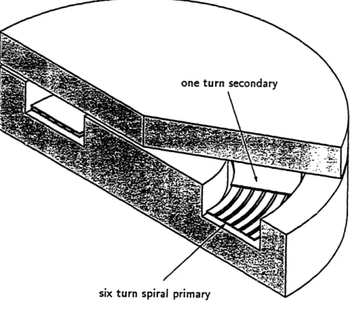
7.4 The Importance of A Single Turn Secondary ... 118
7.5 Dependence of Transformer Size on Frequency ... 119
7.6 Multiple Winding Layers ... 122
7.7 Leakage Inductance and Interwinding Capacitance ... . 126
7.8 Thermal Dependence ... 127
7.9 Scaling Issues ... 131
7.10 Comparison Between Minimum Area Design and Existing ... 133
7.11 Conclusion ... ... 134
Chapter 8 EXPERIMENTAL MEASUREMENTS ON A SLOTTED GAPPED TRANSFORMER ... 135
Chapter 9 CONCLUSIONS AND DIRECTIONS FOR FUTURE WORK ... 139 APPENDICES Appendix A: Appendix B: Appendix C: Appendix D: Appendix E: Appendix F: Appendix G: Appendix H: ... ... .. . . ... .. ... ... .... .... ...
Calculations of Winding Loss ... Calculations of Lumped Parameter Model ... Derivation of Chapter 6 Results ... Material Measurement Software ... Loss in Secondary Winding ... Derivation of Ph/IP, Constraint ...
ZZCHAP7.C ...
Fabrication Techniques ... 142 142 145 149 150 155 156 157 181Chapter 1
INTRODUCTION
While the physical size of digital and analog electronic circuits has been drastically reduced over the past twenty years, the size of their associated power supplies has been reduced at a much slower rate. As a result, the power supply represents an increasing proportion of the size and cost of electronic equipment.1 Recent efforts to miniaturize one common type of power supply, the dc/dc converter, raise the internal switching frequency of the power circuit from the 100-200 kHz range to the 1-10 MHz range in an effort to reduce the size of the energy storage components that dominate the converter volume.
Because of the difficulty of analyzing the power dissipation in the magnetic compo-nents, it has been unclear whether present designs represent the smallest components that can be achieved, or whether their size can be reduced further. The difficulty of analysing both core and copper loss at high frequency has forced designers to make conservative de-signs with cores and windings that may be much larger than they need to be for a given power dissipation. In fact, one prominent member of the power electronics community has written that "...the magnetics design is the main bottleneck to the successful reduction of the overall converter size and weight," and suggests that, because of the limitations of the magnetic components, operation below 500 kHz might yield smaller converters than operation above 1 MHz.2
This thesis, which is part of an MIT project to develop a miniaturized 10 MHz dc/dc converter, investigates the issues involved in miniaturizing magnetic components for dc/dc converters, and employs both theoretical analyses and experimental measurements to develop appropriate designs.3 The work presented in this thesis shows that with careful attention to both core and copper loss, increasing the switching frequency to 10 MHz does indeed reduce the size of the magnetic components.
1 W. W. Burns, III and J. Kociecki, "Power Electronics in the Minicomputer Industry,"
IEEE Proceedings, 76, 4 (1988), pp. 311-324.
2 S. Cuk, Z. Zhang, and L. A. Kajouke, Low Profile, 50 W/in3 Integrated Magnetics PWM Cuk Converter," Technical Papers of the Third International High Frequency Power
Conversion Conference, Intertec Communications, Ventura, California (1988), pp. 442-463.
3 J. G. Kassakian, M. F. Schlecht, "High-Frequency High-Density Converters for Dis-tributed Power Supply Systems," IEEE Proceedings, 76, 4 (1988), pp. 362-376.
1.1 The Need for High Density Dc/Dc Converters
One of the most active areas of research in power electronics today is the development of very high power density dc/dc converters. Dc/dc converters are a basic type of power supply that transform power from one dc voltage and current level to another in order to match power sources with their loads. The new high density converters promise power densities of over 50 W/in3, a ten-fold increase in power density over current technology.4. 5
One application for these miniaturized converters is in equipment whose size and weight must be minimized, such as satellites and aircraft. These aerospace products are produced in low volume, and their performance and reliability take precedence over cost, especially for military applications.
Despite the sophistication of this new technology, these new converters are not limited to application in such speialized, low production volume applications. The converters are small enough to be fabricated by thick and thin film techniques, which permit their mass production and inclusion in high production volume products requiring inexpensive and standardized power supplies. Examples of such high volume products include mid-range and mainframe computers, telecommunications products, and automobiles.
In these products miniaturized power supplies would not just replace present-day equipment, but rather permit the use of a new distributed power supply architecture instead of today's centralized power supplies. In computers, for example, large currents must be bussed at low logic voltages from the centralized power supply to each logic card. In order to avoid ohmic drops in the distribution bus, large and expensive copper bars must be employed. A distributed power supply architecture, made possible by the availability of very high power d3nsity dc/dc converters, would greatly reduce the bus size by distributing power at a higher voltage and lower current than in a centralized power supply architecture. In the distributed architecture the conversion from the bus voltage (typically about 42 V in order to satisfy safety standards) to the logic supply voltage would be performed on each logic board. Since space on tightly packed logic boards is extremely valuable, the dc/dc converter that performs this voltage conversion must be as small as possible.
4 Kassakian and Schlecht
5 F. M. Magalhaes, F. T. Dickens, G. R. Westerman, and N. G. Ziesse, "'Zero-Voltage-Switched Resonant Half-Bridge High-Voltage Dc-Dc Converter," Technical Papers of the
Third International High Frequency Power Conversion Conference, Intertec
15 A <I> = 15A 20A
<I>=1S~~~~A
20i V
Fig. 1.1 Interfacing two dc systems. (Figure reproduced from Principles of Power
Elec-tronics).
1.2 Basic Attributes of the Dc/Dc Converter
This section describes the basic attributes of the conventional, low power density dc/dc converter, explains the role of the magnetic components, and discusses how increasing the internal switching frequency can decrease the volume of the magnetic components.6
A dc/dc converter is a two-port device which connects a power source that provides dc voltage and current to a load that requires its power at a different dc voltage and current. Figure 1.1 shows the basic configuration of such a two-port that connects a source that provides 200 V and 15 A and a load that requires 150 V at 20 A. The two-port must at least-contain a series element to absorb the voltage difference, and a shunt element to balance the current difference. The series element is realized with an ideal switch that continously opens and closes at a fixed frequency. The required dc, or average, voltage across the switch (in this example 50 V) is achieved by choosing an appropriate ratio of its on-time to its off-time (in this example 0.75). This ratio is known as the duty cycle. Similarly, the shunt element is realized with an ideal switch that achieves the required dc, or average, current (in this example 5 A) by opening when the series switch is closed and by closing when the series switch is open. The waveforms of these switches are shown in Fig. 1.2.
Energy storage components must be added to the basic circuit of Fig. 1.1 in order
6 J. G. Kassakian, M. F. Schlecht, and G. C. Verghese, Principles of Power Electronics, Addison-Wesley Publishing Co., Reading, Massachusetts (1989), chap. 6.
- -
<
Vsw>
up
t
-
--<SW
>
t
Fig. 1.2 Switch waveforms showing average values. (Figure reproduced from Principles
of Power Electronics).
to filter the ac components of the switch waveforms, shown in Fig. 1.2, from the source and the load. These additional components are an inductor and capacitor, as shown in Fig. 1.3. These components would have to be infinitely large to remove completely the ac components from the input and output; minimum values for the inductor and the capacitor are determined by the acceptable ripple and the switching frequency.
The minimum value of the inductor can be determined by the following approach. The shunt switch conducts for a period (1-d)/f, where d is the duty cycle of the series switch and f is its frequency. During this conduction interval, the voltage across the inductor is -Vt, so that the current through the inductor will decrease by
which,
solved
for
the
t
dt
(1.1)
which, solved for the inductance, L, gives
L = V (1 - d) (1.2)
Equation (1.2) shows that the value of the inductance required to give a current ripple with an amplitude of AIo,,t/2 is inversely proportional to the switching frequency. Therefore, a higher switching frequency permits a smaller inductance and, assuming that less inductance
A
vsw
--
-~~~~-L
I "~ -'
~~-Fig. 1.3 Minimal topology for a dc/dc converter. (Figure reproduced from Principles of
Power Electronics).
translates into a physically smaller component, a more compact converter. One of the major issues addressed in this thesis is whether the size of the magnetics still decreases as the switching frequency is pushed to 10 MHz.
The general conclusion that the size of the magnetic components decreases with increasing frequency for a given current ripple in this converter, known as the buck converter, also applies to the other commonly used conventional dc/dc converter topologies, such as the boost converter, the forward converter, and the flyback converter. A similar analysis can be performed on the capacitors to show that their size also decreases with frequency for a given voltage ripple.
1.3 The Impact of Parasitic Elements on High Frequency Converters
The new high density converters achieve their volume reduction through the use of switching frequencies above 1 MHz, frequencies which are much higher than those of conventional converters (typically 20-200 kHz). But as the switching frequency is raised above 1 MHz, parasitic energy storage elements, such as switch output capacitance and lead inductance, can cause ringing at transitions which overstress the semiconductor components and become an important source of dissipation. In addition, transformer leakage inductance can introduce load regulation, while transformer interwinding capacitance can introduce a common mode signal path. Both of these effects degrade circuit operation. For this reason, at high frequencies resonant circuit topologies, which seek to incorporate the parasitic energy
r r
0
= ,
I
storage elements in the normal operation of the circuit, are used instead. 7'8 93 10
One representative resonant circuit is the resonant forward converter. This circuit, shown in Fig. 1.4, is used in the MIT miniaturized power supply project of which this thesis research is part." The transformer in this circuit is the subject of detailed design studies that are presented in this thesis. This circuit uses the resonant tank formed by the switch's parasitic output capacitance, C, and the transformer's magnetizing inductance, Lm,,,. As
in the converter described in the last chapter, current flows through diode D, and power is delivered to the load when the switch, Q, is on. When Q9 turns off, the energy stored in the magnetizing inductance of the transformer resonates first into the capacitance across the switch and then back into the magnetizing inductance. The circuit is switched near the tank's resonant frequency, so that Q1 is turned on again when the voltage across the switch and its parasitic capacitance is zero.
The resonant converter, like the conventional converter, requires less inductance at higher frequency, making possible the use of a smaller magnetic component. The depen-dence of the required value of magnetizing inductance on frequency is determined by its relationship to the characteristic impedance and the resonant frequency of the tank. The characteristic impedance, Z, is given by
Z-=I-
C.
M (1.3)and is roughly equal to the ratio of the peak voltage to the peak current in the tank. In order to keep the device stresses constant, this ratio should be held constant as the frequency is increased. The resonant frequency, f,, is given by
f, = 1 (1.4)
7 N. O. Sokal and A. D. Sokal, "Class E - A New Class of High Efficiency Tuned Single-Ended Switching Power Amplifiers," Journal of Solid State Circuits, 10, 3 (1975), pp. 168-176.
8 R. J. Gutmann, "Application of RF Circuit Design Principles to Distributed Power Converters," IEEE Transactions on Industrial Electronics and Control Instrumentation, 27, 3 (1980), pp. 156-164.
9 K. Liu and F. C. Lee, "Resonant Switches - A Unified Approach to Improve Perfor-mance of Switching Converters," IEEE International Telecommunications Energy
Confer-ence Proceedings (1984), pp. 334-341.
10 M. F. Schlecht and L. F. Casey, "Comparison of the Square-Wave and Quasi-Resonant Topologies," IEEE Applied Power Electronics Conference Record (1987), pp. 124-134.
+ Ir . 4 v Lm X11 11 KIll l -L .ll II vout
co
Fig. 1.4 Resonant forward converter.
and should be increased proportionately to the switching frequency in order to maintain the relative timing of the circuit waveforms. Solving (1.3) and (1.4) for L, gives
Z
Em - Z (1.5)
In other words, the inductor's impedance should be held constant. Thus, the required value of inductance in a resonant circuit is inversely proportional to frequency, as in the conventional switching converter.
1.4 The Challenges of Miniaturizing Magnetic Components
Although the use of higher switching frequencies has succeeded in reducing the size of the capacitors, excessive power dissipation in the magnetic components has so far limited their miniaturization. Copper loss is reduced by allocating more core window area for the copper windings, and core loss is reduced by reducing the flux density through making the core larger. As a result, the inductors and transformers currently used still dominate the converter volume and limit the presently achievable converter power density to about 30 W/in3, substantially less than the 50 W/in3 that is considered feasible.2". 3 One of
12 L. F. Casey and M. F. Schlecht, "A High Frequency, Low Volume Point-of-Load Power
Supply for Distributed Power Systems," IEEE Power Electronics Specialists Conference
Record, June 1987, pp. 439-450. 13 Magalhaes, et al. -l I I II II V. ( ) 4 1 I \, 0 - I
the major obstacles to reducing the power dissipation in the magnetic components is the difficulty of analyzing the loss. Without an understanding of the origins of power dissipation, designers are forced to make conservative designs with core and winding geometries that are larger than they need to be for the dissipation that can be tolerated.
Both types of power dissipation, winding loss and core loss, are difficult to analyse. Above 1 MHz skin and proximity effects in the conductors greatly increase the copper loss, but these effects are difficult to analyse in closed form. Although qualitative arguments can be used to develop intuition, accurate computation of the copper loss may require the use of such computation-intensive numerical techniques as finite element analysis. Core loss predictions, unlike copper loss predictions, cannot be made from theory alone, but rather require measured data. Such data is generally unavailable for magnetic materials at these frequencies (1-10 MHz) and flux densities (above 50 G). This lack of data is due, at least in part, to the difficulty of making measurements and interpreting data in the 1-10 MHz range. Parasitic elements can cause large errors in the measurements. Nonuniform flux densities in the cores, together with field-dependent permeabilities, complicate the interpretation of the measured data. So not only must material properties be measured, but the measurement technique itself must be developed.
Even with a thorough understanding of the origins of power dissipation, careful design optimization is necessary in order to achieve the minimum size. The quantitative under-standings of core and copper loss must both be used to design a component that has the required inductance and total dissipation in the minimum possible size. To accomplish this task is one of the most important challenges of this thesis.
Another challenge involves the fabrication of magnetic components. Since the charac-teristic frequency of the resonant circuits used in high frequency converters depends on the value of the energy storage elements, the parasitics that cannot be made negligible must be made highly reproducible. Unlike capacitors, which are sold ready to use, inductors and transformers must usually be assembled from core pieces and magnet wire. A conventional inductor or transformer is made by winding the magnet wire wound around a bobbin and then sliding the bobbin over a post of the magnetic core. These components, which are generally not made by a company specializing in magnetics, but rather put together by a power supply manufacturer, possess parasitic inductances and capacitances that can vary greatly between pieces. The successful development of magnetic components for high fre-quency resonant converters therefore requires designs and fabrication processes that permit economical manufacture to very close tolerances, in order to ensure consistent and small
values for the parasitics. Thick and thin film fabrication techniques not only fulfill these requirements, but also are amenable to economical mass production, unlike wound bobbins which are difficult and expensive to produce.
1.5 Overview of Thesis
The goal of this thesis is the design of easily fabricated, compact magnetic components for the emerging generation of high density power supplies. These components should occupy the minimum circuit board area for a given energy storage and allowable power dissipation. This thesis approaches this goal in several stages.
First, studies are presented that investigate the impact of different core geometries on the copper loss. Although transformer design is the focus of these studies, inductor design is implicitly addressed by discussions of leakage and magnetizing fluxes. Based on considerations of copper loss and ease of fabrication, a core geometry is then selected for the transformer of the MIT prototype high power density converter and a lumped param-eter model of this transformer is developed. Next, the magnetic material selection and core loss are discussed. Nickel-zinc ferrite was chosen as the magnetic material, based on considerations of permeability and core loss. A procedure was developed to experimentally measure the permeability and loss of nickel-zinc ferrites, and to model the dependence of these parameters on the magnetic field. The results of the copper and core loss analyses are incorporated in a computer program that uses sophisticated optimization algorithms to de-sign transformers that provide the necessary energy storage and efficiency in the minimum possible size. A minimum area transformer design for the MIT prototype converter is pre-sented. A transformer with planar spiral windings was then constructed and its properties experimentally measured in order to demonstrate the feasibility of fabricating planar spiral windings, to verify the copper and core loss analyses, and to validate the measurement procedure.
Chapter Two begins the thesis with a discussion of some basic issues of magnetic design, such as whether to use magnetic material, and if so, whether the structure should be gapped.
Chapter Three continues with a survey of previously published work describing at-tempts to make miniature magnetic components. This survey covers the efforts of two engineering communities, signal processing and power electronics, and shows that none of the reported work is appropriate for 1-10 MHz converters.
are discussed. The nature of the proximity effect problem is described and the success of different core geometries in reducing proximity effects and copper loss is investigated with the aid of finite element analysis, a computerized numerical technique.
Chapter Five presents a lumped parameter model for one of the transformers de-scribed in Chapter Four. An approximate formula is derived for each element of the model, which includes all important parasitics. The model is verified by comparison with finite element analyses.
Chapter Six considers the choice and analysis of magnetic materials. A survey of available materials is presented and the choice of nickel-zinc ferrites is explained. An ex-perimental procedure for determining the functional dependence of permeability and loss of the ferrite on the applied field is described, and data for eight different types of Ni-Zn ferrite is presented.
Chapter Seven describes the design studies for a 7:1 transformer intended for the MIT prototype dc/dc converter. These studies combines the analyses of Chapter Four with the material property measurements of Chapter Six in order to perform computer-assisted studies of the design tradeoffs. This chapter discusses such issues as the variation of transformer size with excitation frequency, with total power dissipation, and with the interleaving of multiple winding layers. The tradeoffs between leakage inductance and interwinding capacitance are discussed. The chapter concludes with a design for a 10 MHz converter.
Chapter Eight presents experimental measurements of a representative transformer which was constructed. These measurements serve to validate both the design process and the instrumentation.
Chapter 2
THE USE OF MAGNETIC MATERIAL
Since all of the magnetic components that are discussed in this thesis use magnetic material, it should first be asked whether magnetic material is in fact appropriate for use at 1-10 MHz, or whether air cores should be used instead. This short chapter justifies the use of magnetic material and explains the importance of including an air gap in a structure that stores magnetic energy.
2.1 Magnetic Material. vs. Air Core
One of the initial decisions that must be made in the design of any magnetic compo-nent is whether or not to use magnetic materials. One advantage that magnetic materials provide is flux guidance. In transformers this flux guidance allows a stronger coupling of primary to secondary than is possible with an air core, while in both inductors and trans-formers it greatly reduces stray fields that can induce eddy currents and disrupt circuit operation. But for the dc/dc converter application addressed by this thesis, the most im-portant advantage of using magnetic materials is that for a given total power dissipation, a given inductance can be achieved in a smaller volume.
This section shows the decrease in size that could be achieved if the magnetic material were lossless, so that the only power dissipation would be ohmic loss in the copper windings. The next section discusses how in reality core loss in the magnetic material limits the size decrease that can be achieved and explains how the introduction of an air gap in the core trades off some of the increased inductance per unit volume for less core loss. In this thesis the component size will be characterized by the area, or footprint, that the component would occupy on a printed circuit board, and the component efficiency will be characterized by the ratio of the peak energy stored in the component to the average power dissipated. This ratio is equal to L/R, where L is the component's inductance, and R is the component's resistance. In addition to core loss, the use of magnetic material introduces other problems, such as the dependence of the inductance on the core permeability, which in turn depends on current, temperature, time, and sample. These problems can also be mitigated by the use of an air gap.
This section considers a simple toroidal inductor in order to review the basic argu-ments for using magnetic material. Consider an N turn toroid of inner radius ri, outer radius r, and height h, as shown in Figs. 2.1 and 2.2 (Figure 2.2 is shown with a gap,
Fig. 2.1 Toroidal core with ribbon winding. Shading indicates winding.
permeability of p. The winding is a ribbon whose average width is r(r, + r)/N, so that the N turns fit side by side around the circumference of the toroid, as shown in Fig. 2.1. The ribbon is much thicker than a skin depth, so that for the purposes of computing the copper loss, the effective thickness of the ribbon is one skin depth, .1 In a highly conductive material, such as copper, the skin depth is given by
r 1 (2.1)
where a is the conductivity of the copper.
In order to determine the dependence of the efficiency on the permeability and core size, it is necessary to compute L and R. The inductance is given approximately by
L= N2A (2.2)
where /i is the permeability of the core, N is the number of turns, A is the cross-sectional area of the toroid, and I is the mean magnetic path length of the toroid. This expression is
1 S. Ramo, J. R. Whinnery, and T. Van Duzer, Fields and Waves in Communication
i/
g
Fig. 2.2 Gapped toroidal core. often written as
N2
L = (2.3)
where Rc is the reluctance of the core, given by l/pA. The cross-sectional area of the toroid is given by
A = h(ro - r) (2.4)
and the mean magnetic path is given by
I= 2r (ro + r ) (2.5)
The inductance is therefore given by
L -N hn ri_ ( (2.6)
7r r, + ri
The winc'ing resistance is given approximately by
R = NI,
(2.7)
where lw is the length of each turn and Aw is the effective cross-sectional area of the ribbon winding. The length of each of the N turns is
1t = 2(r, - ri + h) (2.8)
The effective cross-sectional area of the ribbon winding is given by
Aw=
2;r
(ro+
r)
(2.9)
The resistance is therefore
R 2N2 (ro - r + h)(2.10)
arar (ro + ,) (2.10)
The LIR figure of merit can be computed using (2.4) and (2.10) as
R
L i
ro -ri
+)
(2.11)
In order to consider the variation of the toroid's footprint, given by rr2, with , it is
necessary to assume some relationship between the toroid's dimensions. This analysis will simply assume that the aspect ratio of the core remains constant, so that
h r
k k= 2 (2.12)
To - ri r'To
where k, and k2 are constants. Equation (2.11) can be rewritten using (2.12) as
L 18
rT
(kkl(l- k2)) (2.13)This important result, (2.13), shows that if the efficiency is held constant (ignoring core loss), then the footprint, given by r,2, is inversely proportional to 1/2. An air core
would correspond to replacing /z in (2.13) with ,o, so that replacing an air core with a permeable core would decrease the footprint by a factor of (o/j) 2.
2.2 Gapped Magnetic Material
Unfortunately, core loss can not be ignored. For a typical nickel-zinc ferrite operating at 10 MHz, about 20% of the energy stored in the core is lost each cycle. If the inductor must store an appreciable amount of energy, an ungapped core may be prohibitively lossy. In addition, the magnetic material introduces the problems of bu dependence and power loss mentioned above. The section considers the introduction of a small air gap into the core, which can ameliorate these problems.
If a small gap is introduced in the toroidal core, as shown by Fig. 2.2, and the core dimensions are changed so that the gapped and the ungapped cores both provide the same inductance, then the inductance of the gapped core is given by
L 2 (2.14)
IzoA' MA'
where g' is the length of the gap. In (2.14) the dimension are given ' marks to emphasize that these dimensions are different from those of the ungapped core. Commonly, this expression is written as
N2
L = (2.15)
where ~R is the reluctance of the gap, given by g'/uoA', and R is the reluctance of the magnetic material, given by l'/pA'.
The first point is that if R >> R, then the inductance is essentially independent of the value of p, and is given by
lo N2A'
L -- (2.16)
Even if the reluctance of the magnetic material is not negligible, the dependence of the inductance on the permeability is still decreased.
The second point is that for a given inductance and current, introducing a gap reduces the energy stored in the magnetic material, thereby reducing the core loss. This analysis assumes that the core loss is roughly proportional to the energy stored in the core each cycle. The energy stored in the magnetic material of the ungapped core each cycle is given approximately by
W, 1 B2V -21 [/LNi 1A = N2i2 (2.17)
m To -= (2.17)
where V is the core volume and i is the exciting current. The energy stored in the gapped magnetic core is given by
Wmg =
B
2V =2
A(
) ]IA =
+
(
2.18)
Since the inductances of the gapped and ungapped cores have been set equal in this analysis, comparison of (2.3) and (2.15) shows that
R = RI + R (2.19)
Equation (2.18) can therefore be rewritten as
so that the ratio of core loss in the gapped core to core loss in the ungapped core, for a fixed inductance and current, is roughly given by
p=,g _ Wm.g = , = P'/A' (2.21)
P,~, W,, T. -/A
which assumes that the permeability of the core is held constant. In other words, in order for the core loss to be less in the gapped structure than in the ungapped structure, so that
Pc,g/Pc,. is less than unity, the dimensions of the gapped core must be altered so that some of the energy is stored in the gap instead of the core. The impact of this conclusion on the toroidal core considered in this example can be seen by evaluating (l'/A') using (2.4), (2.5), and (2.12), giving
it _ 1
[
7r(l k2)1
(2.22)A' r [k(1 - k2)2 (2.22)
Equation (2.22) shows that in order to reduce l'/A' and reduce the core loss, ri, and hence the footprint, must be allowed to increase. In other words, some of the decrease in footprint that the previous section showed could be gained by using magnetic material must be given up in order to reduce the core loss. A gapped core is still smaller than an air core, however. The decrease in footprint area that can actually be achieved by the use of magnetic material depends on the actual material, and on the core and winding geometry.
2.3 Conclusions
The results of this chapter show that for a given copper loss and neglecting core loss, the use of a magnetic core instead of an air core reduces an inductor's footprint by a factor of
(yo/,u)2. If the inductor has a substantial ac flux component, the core loss may necessitate
the introduction of an air gap and limit the size reduction that the magnetic material would otherwise allow. Since copper loss and core loss both decrease as the inductor footprint is increased, the size reduction that can be achieved is limited primarily by the maximum total power dissipation that can be tolerated.
The analysis presented in this chapter is very approximate, and neglected such fac-tors as proximity effects in the copper, which raise copper loss, and the greater than B2 dependence of the core loss. A ore accurate analysis must await the design studies of
Chapter 7, which make use of the detailed copper and core loss analyses of Chapters 4, 5, and 6. Nevertheless, this chapter shows that gapped magnetic cores promise a higher L/R than air cores.
Chapter 3
PREVIOUS WORK
Efforts to make compact magnetic components have been driven by two different applications, signal processing and power electronics. This chapter briefly surveys the progress that has been made by these two communities. For the applications described in Chapter 7, the component should have an inductance between 1-10 pH. The circuit board area that the component requires, known as the footprint, should be less than 1.0 cm2,
while the height, determined by the spacing between circuit boards, should be less than about 1.0 cm. The ratio of the peak stored energy to the average energy dissipation per cycle, known as the Q, should be greater than about 60. This ratio is equal to wL/R.
3.1 Miniaturized Inductors for Signal Processing
The first efforts to miniaturize inductors for use in the 1-10 MHz range were intended for application to signal processing, primarily for use in tuned filters. While capacitors are easy to fabricate with semiconductor integrated circuit (IC) technology, inductors and transformers are much more difficult to realize. For this reason, small-signal inductance was achieved by devices that simulated a reactive impedance, such as active transistor circuits' and transit-time diodes.2
The first IC devices for actual magnetic energy storage were formed by the deposi-tion of thin films (0.1 pm) of permalloy, a nickel-iron alloy, on a silicon substrate. The skin depth of permalloy at 1 MHz is about 2 pm, so that eddy current losses were negligible in the 0.1 pm films. In 1979 Soohoo proposed, but did not fabricate, a planar structure com-posed of a planar spiral of evaporated copper conductor embedded between two sputterred permalloy films.3 A similar structur~ was fabricated in 1984 by Kawabe et al., in which a meander line, illustrated in Fig. 3.1, was used instead of a planar spiral.4 Presumably
I S. Noguchi, "Solid State Inductor Using Hybrid IC and its Characteristics,"
Proceed-ings of the Fourth International Symposium on Hybrid Microelectronics, (1974), pp. 60-66.
2 S. M. Sze, Physics of Semiconductor Devices, 2nd ed., John Wiley and Sons, Inc.,
New York (1981), pp. 579-585.
3 R. F. Soohoo, "Magnetic Thin Film Inductors for Integrated Circuit Applications,"
IZEE Transactions on Magnetics, 15, 6 (1979), pp. 1803-1805.
4 K. Kawabe, H. Koyama, and K. Shirae, "Planar Inductor," IEEE Transactions on
Magnetics, 20, 5 (1984), pp. 1804-1806 (Page numbers are indeed close to those of previous
U
U
II
Fig. 3.1 Meander line.
the meander line, familiar from microwave devices, was substituted in order to avoid the difficulty of connecting the center of the planar spiral to the periphery of the device. While the device had a fairly large footprint of 1.4 cn 2, its height was only 20 yIm. Unfortunately, this device functioned more as a resistor than an inductor. At 1 MHz the component had an inductance of 100 nH and a resistance of 10 2, for a Q of only 0.06. Despite further attempts at improving this approach, the authors were only able to increase the Q by a factor of two.5 '6
The cloth inductor was an innovative device in which the windings were literally woven together with strands of amorphous magnetic metal, as shown in Fig. 3.2. 7. 8 For clarity, the structure can be approximated as many parallel solenoids, as shown in Fig. 3.3. Unfortunately, for reasons of fabrication, the threads of amorphous metal used
O0. Oshiro, H. Tsujimoto, and K. Shirae, "A Closed-type Planar Inductor," IEEE
Translation Journal on Magnetics in Japan, 2, 4 (1987), pp. 329-330.
6 0. Oshiro, K. Kawabe, H. Tsujimoto, and K. Shirae, "A Wide Frequency Planar Inductor," IEEE Translation Journal on Magnetics in Japan, 2, 4 (1987), pp. 331-332.
7 H. Matsuki and K. Murakami, "A New Cloth Inductor Using Amorphous Fiber,"
IEEE Transactions on Magnetics, 21, 5 (1985), pp. 1738-1740.
8 H. Matsuki, K. Murakami, and T. Yamamoto, "Preparation and Characteristics of
Cloth Inductor," IEEE Translation Journal on Magnetics in Japan, 2, 4 (1987), pp.
324-326. i M I I I
0
InC ~Fig. 3.2 Cloth inductor (Matsuki, Fig. la).
by Matsuki and Murakami in their original work had diameters of 80 yum, much larger than the material's skin depth at 1 MHz, 6 ,/m. For this reason the eddy current loss in the amorphous metal was severe. The cloth inductor they fabricated had an inductance of 80 IH at 1 MHz, but a resistance of 280 Q, giving the very low Q of 1.8. The authors were able to improve this performance in later work by using threads with diameters of only 20 Im, producing an 8 IH inductor with a resistance of 2.5 Q2 at 1 MHz.9 The footprint of this inductor was only 0.1 cm2, and the height only 4 mm. The Q of this new device was 20, an order of magnitude improvement over the original device. This loss, however, is still much too high for power applications, and the loss will only increase above 1 MHz, since the skin depth will decrease. The authors suggest that 1 MHz is the maximum usable frequency for the cloth inductor.
The most successful of the attempts to miniaturize inductors was the cylindrical chip inductor. °0 In this structure, shown in Fig. 3.4, a "barrel winding" is cofired inside a
nickel-0 H. Matsuki, K. Murakami, and T. Yamamoto, "Performance of Miniaturized Mag-netic Devices in Cloth Structure," IEEE Transactions on MagMag-netics, 22, 5 (1986), pp. 415-417.
10 T. Hirai, Y. Hamazama, T. Ishida, T. Honda, T. Masumyama, "Cylindrical Chip Inductors," International Journal of Hybrid Microelectronics, 4, 2 (1981), pp. 96-99.
Fig. 3.3 Approximation to cloth inductor (Matsuki, Fig. lb).
Internal Conductor
External
T
Ferrite Material
Fig. 3.4 Cylindrical chip inductor (Hirai, Fig. 3).
zinc ferrite. This device is essentially an ungapped pot core. Hirai et al. were able to fabricate an inductor that at 10 MHz displayed an inductance of 1.6 pH and a resistance of 2.1 fl, for a Q of 48. Moreover, the footprint was only 0.13 cm2 and the height only 2.2 mm.
While encouraging, this device is unsatisfactory for three reasons. First, the fabri-cation is difficult. The ferrite shrinks during cooling, which can cause defects. Moreover, the ferrite must be fired at temperatures between 900-1200°C. This precludes the use of
copper windings, since copper would oxidize. Metals with lower conductivities must be used instead, such as silver (used by Hirai). The second problem is that in this structure proximity effects in the conductors have greatly increased the copper loss and reduced the Q. This problem will be described in great detail in Chapter 4, together with a discussion of structures that avoid the problem. The third problem is that the magnetic energy is stored in the magnetic material, instead of in an air gap. As explained in Chapter 2, at power flux levels the resulting core loss would greatly reduce the Q.
3.2 Miniaturized Transformers for Dc/Dc Converters
Power electronic applications have focussed on the development of miniaturized trans-formers, rather than inductors, since, as shown in Fig. 1.4, the inductances required in dc/dc converters can often be combined with the transformers. Published work to date reflects initial attempts to address some of the requirements of high frequency conversion.
One of the first power transformers to use printed circuit board windings was con-tained in the Analog Devices AD293/4, a 200 kHz hybrid flyback converter." In this trans-former the primary and secondary windings were planar spirals printed as multiple layers on an alumina substrate. The alumina in the center of the spirals was cut out and the windings were fitted around the center leg of a manganese-zinc ferrite E-core. Although the switching frequency was only 200 kHz, the transformer demonstrated that thick film techniques could greatly improve the manufacturability of the transformer windings. Five years later, a similar design was implemented for a 1 MHz resonant converter produced by Theta-J Corporation.' 2 This very large transformer had a footprint of 10 cm2 and a height of 1.8 cm.
In one of the earliest papers on megahertz range dc/dc converters, Gutmar. suggested that above 1 MHz inductors might be formed simply from printed spirals, without magnetic material.l 3 Such two-dimensional inductors were analyzed in detail by Rodriguez et al., who fabricated a 3 uH planar spiral inductor with a footprint of 4.9 cm2, and measured its Q
1 D. Bokil and W. Morong, "Thick-film Transformer Advances Hybrid Isolation Am-plifier," Electronics, August 25, 1981, pp. 113-117.
12 A. Estrov, "1-MHz Resonant Converter Power Transformer is Small, Efficient,
Eco-nomical," Power Conversion and Intelligent Motion, August 1986, pp. 14-24.
13 R. Gutmann, "Application of RF Circuit Design Principles to Distributed Power
Converters," IEEE Transactions on Industrial Electronics and Control Instrumentation, 27, 3 (1980), pp. 156-164.
as 38 between 1-10 MHz. Due to the large footprint and low Q, Rodriguez found that "...it is unlikely that such a structure will be adequate to store sufficient energy for power applications." 1 4
Recent work has attempted to integrate the ferrite magnetic material into the thick film hybrid fabrication process. A 500 kHz thick film hybrid buck converter produced by Fuji Electrochemical Co. was fabricated on a nickel-zinc ferri'te sbstrate, instead of the usual alumina substrate.15 However, the windings of the buck converter's current source inductor were not printed with thick film. Instead, windings of ordinary magnet wire were wrapped around a notched tab of the substrate. This tab had a surface area of about 1,4 cm2 and a thickness of 0.8 cm. Gradski fabricated a transformer whose windings were printed with multiple layers of thick film on a ferrite substrate for a 6 MHz resonant forward converter.'6 This design achieved a magnetizing inductance of 1.3 JLH, but the resistance to the magnetizing current was too large, 2.5 at 10 MHz, giving a Q at that frequency of only 33. The resistance, measured at an extremely low flux level, also does not reflect the additional core loss that would be present at power flux levels. The large resistance to the magnetizing current is in large part due to proximity effects in the conductors that occur because the windings are in the gap of this transformer. This effect will be discussed in more detail in Chapter 4. Gradski closed the magnetic circuit by covering the printed windings with half of a standard pot core. This pot core, the TDK RM5, has a footprint of 1.5 cm2, and the core and substrate have a total height of about 1.6 mm. Both the footprint and height are too large. Efforts to print instead thick film ferrite layers on top of the windings, in the same fashion as insulating dielectric layers, were notably unsuccessful, due to the basic incompatibility of the thick film process with the high sintering temperatures of ferrite.'7
Other transformer designs focussed on controlling parasitics that affect high frequency converter topologies, such as leakage inductance. For example, the dual forward converter
14 R. Rodriguez, J. M. Dishman, F. T. Dickens, and E. W. Whelan, "Modeling of
Two-Dimensional Spiral Inductors," IEEE Transactions on Components, Hybrids, and
Manu-facturing Technology, 3, 4 (1980), pp. 535-541.
1S N. Kato, S. Hirano, and M. Torii, Ferrite Substrates for High-Frequency Switch-ing Dc-To-Dc Converter Applications," IEEE Transactions on Magnetics, 21, 5 (1985), pp. 1723-1725.
16 P. M. Gradski and F. C. Lee, "Design of High-Frequency Hybrid Power Transformer,"
IEEE Applied Power Electronics Conference Proceedings, February 1988, pp. 319-326. 17 P. A. Gradski, "High Frequency Magnetics," Virginia Power Electronics Center
Core
Seco
Primai
Insulator W-.,4+ C;. I, I IdL J111%Fig. 3.5 Low leakage transformer incorporating output diodes into secondary (Carsten,
Fig. 9).
cannot tolerate leakage inductance, since it delays the commutation of current from one output diode to the other. For that circuit Carsten designed the low leakage transformer of Fig. 3.5, which incorporates the output diodes into the secondary winding.'8
Some resonant circuits, on the other hand, require a large leakage inductance that must function as part of a resonant tank. The transformer of Fig. 3.6 was used in the Vicor Corp. VI-200, a 1 MHz resonant converter.' 9 This transformer achieved a very high leakage inductance by using a toroidal winding for the secondary.
3.3 Conclusions
The work reported to date has not produced magnetic components that meet the requirements of the new generation of high power dc/dc converters. The magnetic
compo-18 B. Carsten and M. Chirea, "A Low Voltage Schottky for High Efficiency VLSI Power
Supplies," Official Proceedings of the Ninth International Power Conversion International
Conference, Intertec Communications, Ventura, California (1984), pp. 323-338.
1 S. D. Cogger, "Dc-to-dc Converter Family Packs Power Into Tight Spots," Electronic
- , _ Base Plate Primary
a a r
Fig. 3.6 High leakage transformer (Cogger, Fig. 2).
nents fabricated for signal processing applications are too lossy for power applications. The components designed for switching power converters were intended for application at 1 MHz and below and their designs cannot be easily extended for higher frequency operation. Their magnetic materials have been too lossy, their parasitics too large, and their windings have been subject to proximity effects and excessive copper loss. However, the Analog Devices and Theta-J transformers both demonstrated that the replacement of conventional magnet wire windings with thick film printed windings can greatly improve the manufacturability of magnetic components.
While the components described in this chapter represent important preliminary research, the work that produced them does not constitute an organized effort to identify the underlying limits to the miniaturization of these components and determine the levels of performance that can be achieved. This thesis attempts to address these issues and presents in Chapter 7 a design for a 10 MHz transformer with a footprint of 0.34 cm2 and a height of 2.5 mm. The magnetizing inductance of this transformer is 1.33 /LH, and the Q of the magnetizing inductance at the specified magnetizing current of 0.75 A is 71.
Chapter 4
DISCUSSION OF MAGNETIC COMPONENT GEOMETRY
The goal of this chapter is to choose a geometry for the magnetic component that stores a given amount of energy with the minimum copper loss. Several different geometries are examined and compared. The results of these studies are used in Chapter 7, which addresses the ultimate goal of designing transformers that have the minimum size for a given energy storage and power dissipation. As explained in the introduction, although this chapter considers transformers, since this is the component required for the MIT prototype converter, inductors are implicitly addressed by discussions of leakage and magnetizing fluxes. This chapter develops a transformer geometry, the slotted gapped transformer, that represents a reasonable compromise between low copper loss and fabrication complexity.
Careful design is required to minimize the total core and copper loss for a given transformer volume. For the core loss, the most difficult task is to understand its dependence on flux level, frequency, and dc bias. These issues of selection and characterization of the magnetic material will be addressed in Chapter 6. For the copper loss, the most difficult task is to understand the relationship between the current distribution and the transformer structure. Without an adequate understanding of this relationship, a structure that has an unexpectedly high copper loss due to skin and proximity effects might be designed. This chapter therefore focusses on the relationship between transformer structure and copper loss.
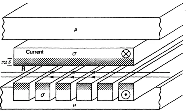
Unfortunately, the magnetic diffusion equation that describes the current distribution is difficult to solve for the transformer structures considered here. This thesis therefore develops qualitative understandings of the field and current distributions and employs finite element analyses to produce numerical solutions. The finite element method and software are briefly described.
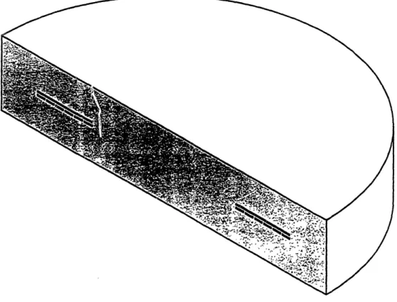
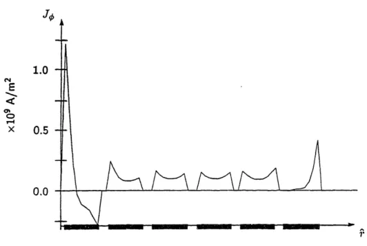
The first structure considered is a simple sandwich transformer composed of a planar winding pressed between two plates of magnetic material, shown in Fig. 4.1. Although the sandwich structure is very simple to manufacture, the copper loss is greatly increased by circulating currents that are induced in each turn by the proximity of the magnetizing current in the other turns. The origin of these circulating currents, whose presence is known as the "proximity effect", is explained in detail, and a finite element analysis showing their distribution is presented.
In the sandwich transformer magnetic material surrounds a planar loop of conductor. Another way of constructing a simple magnetic circuit is for the conductor to surround a
Fig. 4.1 Cutaway view of sandwich transformer with planar spiral winding.
planar loop of magnetic material, as in Fig. 2.1. If energy had to be stored in the structure, a gap could be added, as in Fig. 2.2. Instead of winding wire around the toroid, the windings could be composed of printed sections on the toroid's top and bottom surfaces that are connected by a piece of flexible printed circuit wrapped along the toroid's inner and outer edges. This complicated arrangement, pictured in Fig. 4.2, is necessary because printed circuits are essentially two dimensional, while the winding around the toroidal core is essentially three-dimensional. It is much simpler to make the sandwich transformer and structures like it, since they require essentially two-dimensional winding patterns. Toroidal structures will therefore not be considered here.
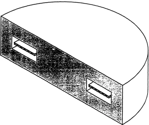
Since the sandwich transformer, while relatively easy to fabricate, has high copper losses, three alternative transformer structures are examined. Although these structures are more complicated to fabricate than the sandwich transformer since they require more com-plicated core shapes, their geometry serves to minimize the magnetizing current proximity effects and the resulting copper loss. These alternative structures are the cofired trans-former of Fig. 4.3, the slotted gapped transtrans-former of Fig. 4.4, and the slotted ungapped transformer of Fig. 4.5. The cofired transformer is formed by both eliminating the air gap
windings
Fig. 4.2 Toroid with thick film windings on top and bottom and flexible printed circuit board connections at inner and outer edge.
and completely embedding the conductors in a lower permeability material, forming a un-gapped structure. In the slotted un-gapped transformer the windings are recessed in a deep slot, forming a structure similar to a pot core. The slotted ungapped transformer is formed by eliminating the gap in the slotted gapped transformer and using a lower permeability material in order to maintain the same reluctance.
For each structure, finite element analyses were used to determine the magnetic field distribution and the effective ac resistance of the windings to the magnetizing current. Studies are presented that examine the dependence of the copper loss on the transformer dimensions in order to understand the tradeoff between increased transformer size and decreased copper loss.
These studies, which seek to minimize the copper loss when only the magnetizing current is present, are incomplete, since the copper loss in a transformer depends on the total current in the windings. This current is the sum of the magnetizing current, the load current, and any currents due to interwinding capacitances. This analysis neglects such currents,
Fig. 4.3 Cutaway view of cofired transformer with planar spiral winding.
which are shown in the next chapter to be small. The two significant components of the current, the load current and the magnetizing current, may be distributed very differently in the conductors. The loss associated with a particular design therefore depends very strongly on the relative magnitudes of the magnetizing and load currents. In order to prevent the results presented here from depending on specific values of magnetizing and load current, the different transformer designs were evaluated by comparing the dissipations that would have resulted if only the magnetizing current were present. This chapter will show that the load current would have the same distribution in each structure that was investigated. Since computing the copper loss due to the magnetizing and load currents separately does not necessarily give the correct value for the total copper loss, the analysis assumes that a reduction in the magnetizing current proximity effect is beneficial. This assumption is reasonable for a gapped transformer, since the magnetizing current is generally substantial.
Another complicated issue is the distribution of the magnetizing current between primary and secondary. The amount of magnetizing current that flows in each winding
depends in large part on the external circuit. For simplicity, this thesis assumes that the magnetizing current flows entirely in the primary. The intent of this chapter is to show
Fig. 4.4 Cutaway view of slotted gapped transformer with planar spiral winding. what must be done to minimize the proximity effects, regardless of the detailed nature of the winding currents.
The work in this chapter shows that while in a simple sandwich transformer the ac resistance can be over eight times the dc resistance, by using such structures as the gapped slotted transformer, it is possible to reduce the ac resistance to the point where it is only 33% more than the dc resistance. This number, 33%, represents the smallest ac resistance that can be achieved with the structures discussed in this chapter, and is reached at the expense of a larger transformer. The nature of the tradeoff between size and loss is discussed later in this chapter.
4.1 Finite Element Analysis
The magnetic diffusion problems posed by the structures in this chapter were solved by means of finite element analyses. This section briefly describes the procedure used by
Fig. 4.5 Cutaway view of slotted ungapped transformer with planar spiral winding. the finite element analysis computer program used in this thesisl.
First, the program breaks up the geometry of the problem into a mesh of triangles. The program treats the transformers as being axisymmetric, so that the problem is reduced from three dimensions (r, , z) to two dimensions (r, ). The length of each triangle side must be much shorter than the characteristic length of the solution in that region. For example, in the conductors the characteristic length is a skin depth, so that the sides of the triangles there must all be much shorter than a skin depth. The solution is computed at each vertex and midpoint; these positions are called nodes. Quadratic interpolation is used to determine the solution between nodes. Material properties are associated with triangles, sources are defined, and boundary conditions are imposed. It should be noted that this software models the permeability as a real constant, so that its solutions do not take into account either core loss or the variation of permeability with flux level.