HAL Id: hal-01006121
https://hal.archives-ouvertes.fr/hal-01006121
Submitted on 13 Jun 2014
HAL is a multi-disciplinary open access
archive for the deposit and dissemination of
sci-entific research documents, whether they are
pub-lished or not. The documents may come from
teaching and research institutions in France or
abroad, or from public or private research centers.
L’archive ouverte pluridisciplinaire HAL, est
destinée au dépôt et à la diffusion de documents
scientifiques de niveau recherche, publiés ou non,
émanant des établissements d’enseignement et de
recherche français ou étrangers, des laboratoires
publics ou privés.
Effect of Electrical Stresses on Digital Integrated
Circuits Power Integrity
Alexandre Boyer, Sonia Ben Dhia
To cite this version:
Alexandre Boyer, Sonia Ben Dhia. Effect of Electrical Stresses on Digital Integrated Circuits Power
Integrity. 2013 17th IEEE Workshop on Signal and Power Integrity (SPI), May 2013, Paris, France.
pp.1-4. �hal-01006121�
Effect of Electrical Stresses on Digital Integrated
Circuits Power Integrity
A. Boyer, S. Ben Dhia
LAAS-CNRS
Université de Toulouse ; UPS, INSA, INP, ISAE ; UT1, UTM, LAAS Toulouse, France
Abstract—Recent studies have shown that integrated circuit
aging modifies electromagnetic emission significantly. The proposed paper aims at evaluating the impact of aging on the power integrity of digital integrated circuits and clarifying its origin. On-chip measurements of power supply voltage bounces in a CMOS 90 nm technology test chip are combined with electric stress to characterize the influence of aging on power integrity. Simulation based on ICEM modeling modified by an empirical coefficient in order to take into account the circuit aging is proposed to model the evolution of the power integrity induced by device aging.
Keywords— Integrated circuits, power integrity, accelerated aging, ICEM modelling
I. INTRODUCTION
Recently, many publications have forecast a decrease of new CMOS technology device lifetime down to few years [1], with anticipated appearance of hard or soft failures due to wear-out mechanisms (e.g. hot carrier injection, negative bias instability, electromigration…) [2] [3]. The drift of the electrical characteristics of semiconductor devices can have direct consequences on integrated circuit electromagnetic emission and power integrity (PI). Recently, some publications have shown that accelerated aging tests such as high or low temperature operating life, thermal cycling, or electrical overstress induce a significant variation of electromagnetic emission produced by power supply units [4], high side switch devices [5] or I/O buffers [6]. However, these studies do not address the evolution of power integrity and do not clarify the origins of emission change.
This paper intends to clarify the impact of IC aging on PI experimentally and by simulation. A test chip designed in Freescale CMOS 90 nm technology, which includes a digital core and on-chip sensors dedicated to the measurement of power supply voltage fluctuations, has been developed to characterize the evolution of PI vs. time. In order to explain the effect of IC aging on power integrity, an equivalent model of the circuit based on the Integrated Circuit Emission Model (ICEM) approach [7] is developed to simulate the PI. A simple empirical coefficient is introduced in the model to simulate the evolution of the PI with time. The paper is organized as follows: after a description of the circuit under test, on-chip sensors and experimental set-up, the measurements of the
evolution of the power supply voltage bounces are presented. Then, the proposed modeling approach of the circuit power PI is described and, finally, simulation and measurement results are compared in order to validate both our hypothesis about PI evolution with time and the proposed model.
II. EXPERIMENTAL SET-UP A. Test chip description
A dedicated test chip has been designed in Freescale CMOS 90 nm technology for IC emission and susceptibility modeling, and characterization of aging impact on EMC of ICs. In particular, the test chip includes a digital core with a dedicated power supply voltage equal to 1.2 V. This structure is a basic 100-stage shift register, synchronized by a 40 MHz clock.
B. On-chip voltage sensor
In order to monitor the voltage drops on the power supply of the digital core, an on-chip voltage sensor is placed along the power supply rail of the core. This sensor is able to measure the waveform of voltage bounce across non accessible nodes with a precise time resolution (up to 15 ps). Its analog bandwidth is equal to 10 GHz. Its principle and its implementation in the test chip are explained in [8]. In order to prevent noise coupling with the digital core, the designed sensor has a dedicated power supply and is isolated from the IC substrate by a buried N layer. Due to its small input capacitance (4 fF), the sensor is not intrusive and does not alter the performance of the tested block. Although the electrical stress applied to the circuit under test can partially alter the performances of the sensor, it can be recalibrated before any measurements. The calibration process is necessary to compensate effects of imperfections due to non ideal behavior and mismatch on voltage and frequency responses.
C. Description of the experimental set-up
The experiment is based on a measure-stress-measure flow, which consists in applying electrical stress on the circuit under test and interrupts the stress during short period regularly for characterization purpose. With this procedure, the characteristics of the circuit are monitored at various degree of aging.
The choice of stress conditions (stress voltage and duration) is based on a preliminary failure analysis of MOS devices developed in this technology [9] [10]. For DC stress voltages ranging from 3 to 4 V and applied between drain and source of NMOS and PMOS devices, significant degradations of threshold voltage and carrier mobility are induced due to HCI and/or NBTI after several hundreds of seconds. The amount of degradation is related to stress voltage, duration, transistor geometry and gate oxide thickness. A 3.6 V electrical stress is applied during 120 minutes in order to validate the influence of the stress voltage on power integrity change. Sensor measurements of power supply voltage fluctuations are performed after each stress interval. The sensor is not supplied during stress phases in order to reduce its aging. Recalibration is done after each stress period, although experimental characterizations have not shown any significant degradation of the sensor.
III. EXPERIMENTAL RESULTS: EVOLUTION OF POWER INTEGRITY AFTER ELECTRICAL STRESS
A. Initial measurement of power integrity
Fig 1 presents the power supply voltage fluctuations produced by the digital core activity measured by the on-chip sensor. Positions of clock edges are indicated. Rapid droops appears at each clock switching. These events are linked to the rapid current demand from every gates and latches of the core. A damped oscillation with a pseudo-period equal to 4.5 ns follows the first rapid current impulsion. It is linked to the anti-resonance produced by on-chip capacitor and package inductor (see part V for more details). This type of noise is also measured on Vss node. Similar voltage fluctuations are also measured on the ground node of the circuit.
Fig. 1. Measurement of the power supply voltage bounce of the digital core
B. Impact of electrical stress on digital core power integrity
After stress, the core remains operational and its quiescent current has not changed. However, the core timing characteristics have evolved. A specific part of the core has been designed to measure the propagation delay through one D-latch and 100 inverters. The propagation delay through the core after stress increases up to 31 % depending on the stress duration. The electrical stress applied on core power supply accelerates wear-out mechanisms such as HCI and/or NBTI. They increase the propagation delay of each gate of the core.
Fig. 2 presents the power supply voltage bounces measured by the on-chip sensor before and after 3.6 V stresses. A -30 % reduction of the peak-to-peak amplitude is observed d. The waveform of the signal is also modified. The first peak is less steep. The period of the resonance oscillation has not changed. Its amplitude is reduced, but it is still damped at the same rate. This observation indicates that the package inductance, the equivalent capacitance of the digital and resistance linked to the power distribution network (PDN) have not been affected by the electrical stress significantly.
59 mV
42 mV
Fig. 2. Evolution of the corepower supply voltage bounce after 120 minutes of 3.6 V electrical stress
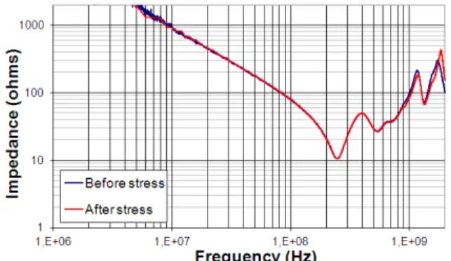
This hypothesis is confirmed by impedance measurement of the PDN with a vector network analyzer, as shown in Fig. 3. Whatever the electrical stress amplitude and duration, the impedance of the circuit power distribution network remains constant over a large frequency range.
Fig. 3. Measurements of the impedance of the power distribution network of the digital core before and after electrical stress
From these experimental results, the following hypothesis can be proposed to explain the evolution of power integrity of the circuit: the reduction of power supply voltage bounce is only linked to the change of transient current produced by the core activity. Wear-out mechanisms accelerated by electrical stress have reduced mobility of carrier in MOS devices so the switching transient current has been spread. The consequence is a reduction of the high frequency content of the switching transient current, which has a direct impact not only on power integrity but also on conducted emission. The next part intends to validate this hypothesis by the modeling of the evolution of the power integrity due to circuit aging.
IV. MODELING OF DIGITAL CORE AGING EFFECT ON POWER INTEGRITY
A. Model construction and validation
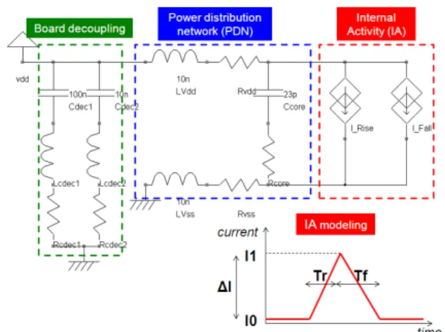
The model construction is based on ICEM approach [7]. The model includes two main parts: the internal activity (IA) block which models the transient current produced by circuit operation, and the power distribution network (PDN) which models the filtering effect of the transient current due to IC and package.
A linear model based on an equivalent RLC circuit is proposed for the PDN. The parameters of the model are extracted from measurements. The passive element values are fitted from an impedance measurement between Vdd and Vss pins of the digital core made with vector network analyzer, as shown in Fig. 3. A very simple approach is used for IA modeling: two triangular waveform current sources describe the current produced at each clock edge. Even though such a waveform is quite simplistic, it provides a good estimation of the actual current waveform which can be tuned without a precise analysis of the circuit power consumption. The waveforms of the IA current source are fitted from current and Vdd bounce measurements. For each current source, only four parameters are adjusted: current peak minimum and maximum I0 and I1, rise and fall times Tr and Tf of the peak. Fig. 4 presents a simplified structure of the ICEM model of the digital core.
Fig. 4. ICEM model of the digital core
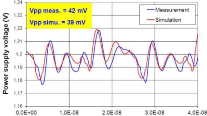
SPICE transient simulations are performed to compute the waveform of the power supply of the digital core and extract the peak-to-peak amplitude of the voltage fluctuation. Fig. 5 presents a comparison between measurement and simulation of the power supply voltage bounce before electrical stress. The simulated waveform is similar in term of peak-to-peak amplitude, pseudo-oscillation period and damping. Although the correlation between measured and simulated curves is not totally perfect, the model offers a sufficient accuracy for the aim of the study. A better correlation would rely on a more complex transient current waveform, extracted from a precise analysis of the power consumption of the digital core.
B. Simulation of electrical stress impact on power integrity
Wear-out mechanisms accelerated by electrical stress tends to degrade carrier mobility and threshold voltage of MOS devices which constitutes the gates of the digital core. It leads to a reduction of the saturation current of MOS devices and an increase of the propagation delay. In other words, it leads to a spreading of the current pulse induced by the switching of the gates of the digital core. However, as the charge transfer associated to each gate switching does not change after stress, the product between current pulse duration and current pulse amplitude remains constant.
Fig. 5. Comparison between measurement and simulation of the digital core power supply voltage bounce before electrical stress
In order to take into account the aging of the circuit in the ICEM model, the following simple methodology is proposed. Only three parameters of the equivalent current sources in IA block are changed to spread the current pulse created by the digital core: the rise and fall times Tr and Tf of the current pulse are increased while its amplitude i is reduced by an empirical coefficient δ called “degradation ratio”, as shown by equations 1 and 2. If δ is equal to 0, it means that the digital core is not degraded and the current pulse is not spread. If δ increases, a larger amount of degradation is considered and the current pulse is spread. In our ICEM model, the same degradation ratio is applied on both current sources of the IA block.
istress = iinitial.(1-δ), 0 ≤ δ ≤ 1 (1)
tr stress = tr initial/(1-δ), 0 ≤ δ ≤ 1 (2)
By simulation, the effect of δ on the power integrity can be studied. A first study consists in finding the peak-to-peak amplitude of the power supply voltage fluctuation vs. the applied δ. Fig. 6 presents the evolution of the peak-to-peak amplitude of the power supply bounce when δ is increased in both current sources symmetrically. The result confirms that the power supply bounce is reduced when the current pulse is spread. However, we need to confirm that our approach is able to model the evolution of the power supply voltage waveform correctly by a comparison with the on-chip measurements done in stressed cores.
Fig. 6. Simulated evolution of the peak-to-peak amplitude of the power supply voltage bounce vs. degradation ratio
Although the coefficient δ is empirical and its value for a given amount of stress is unknown initially, the curve shown in Fig. 9 can help us to choose a reasonable value. From on-chip measurement results, a value of δ is selected to obtain the same voltage fluctuation amplitude. Fig. 7 presents the comparison between the measurements and simulations of the power supply voltage bounces before and after the stress condition described in part II.C. The coefficient δ is set to 0.58 to model the effect of the 3.6 V stress applied for 120 minutes. The correlation between measurement and simulation curves is acceptable. Our basic ICEM model modified by the empirical degradation ratio is able to reproduce the evolution of the power supply voltage bounce with a reasonable accuracy.
These results confirm the relevance of our hypothesis about the origin of the evolution of the power integrity after circuit aging accelerated by an electrical stress. The degradation mechanisms induced a MOS device level tends to spread the current pulse produced by the switching of the gates of the digital circuit, leading to a decrease of the power supply voltage bounce. Moreover, these results demonstrate that the evolution of the power integrity can be predicted by a correct modeling of the change of the circuit current consumption. A complex methodology based on an accurate prediction of the power consumption from the circuit netlist combined with the modeling of MOS device degradation mechanisms could provide an accurate estimation of the evolution of the power supply voltage bounce. However, a more simple and non confidential approach based on an ICEM model affected by an empirical coefficient to take into account the IC aging can also provide a reasonable estimation of the evolution of the power integrity.
V. CONCLUSION
The proposed paper aims at clarifying the impact of circuit aging on power integrity. Electrical stresses applied on a digital circuit lead to a reduction of the power supply voltage bounce. This improvement is linked to a change of the transient current linked to the circuit activity. This hypothesis has been confirmed by the modeling of the circuit activity based on ICEM approach. The impact of the electrical stress on the transient consumption is modeled by an empirical coefficient. This basic and non confidential model reproduces the power
supply voltage bounces with an acceptable accuracy. This type of modeling approach could also be used to predict the evolution of conducted emission from digital integrated circuits, as shown in [6].
Fig. 7. Comparison between simulated power supply voltage bounce after 120 minutes of 3.6 V electrical stress
ACKNOWLEDGMENT
The authors would like to thank Bertrand Vrignon and John Shepherd from Freescale Semiconductor, Toulouse, for test chip development and their constant support.
REFERENCES
[1] J. Srinivasan, S. V. Adve, P Bose, The impact of technology scaling on lifetime reliability”, The International Conference on Dependable Systems and Networks, (2004).
[2] J. W. McPherson, “Reliability trends with advanced CMOS scaling and the implications for design”, 2007 IEEE Custom Integrated Circuits Conference (CICC).
[3] M. White, Y. Chen, “Scaled CMOS technology reliability user’s guide”, NASA WBS 939904.01.11.10, 2008, http://nepp.nasa.gov.
[4] I. Montanari, A. Tacchini, M. Maini, “Impact of thermal stress on the characteristics of conducted emissions”, 2008 IEEE Int. Symposium on Electromagnetic Compatibility, EMC 2008, Detroit.
[5] A. Boyer, A. C. Ndoye, S. Ben Dhia, L. Guillot, B. Vrignon, “Characterization of the evolution of IC emissions after accelerated aging”, IEEE Trans. on EMC, vol. 51, no 4, Nov. 2009, pp 892 – 900. [6] S. Ben Dhia, A. Boyer, B. Li, A. C. Noye, “Characterization of the
electromagnetic modelling drifts of a nanoscale IC after accelerated life tests”, Electronic Letters, 18th February 2010, Vol. 46, no. 4, pp. 278-279.
[7] IEC62433-2, “Models of Integrated Circuits for EMI behavioral simulation – ICEM-CE, ICEM Conducted Emission Model”, International Electrotechnical Commission, Geneva, Switzerland, 2006 [8] A. Boyer, S. Ben Dhia, C. Lemoine, B. Vrignon, “Characterizing circuit
susceptibility with on-chip sensors”, 2012 Asia-Pacific Int. Symposium on Electromagnetic Compatibility, May 2012, Singapore.
[9] B. Li, N. Berbel, A. Boyer, S. Ben Dhia, R. Fernandez-Garcia, “Study of the impact of hot carrier injection to immunity of MOSFET to electromagnetic interferences”, Microelectronics Reliability, vol. 51, 2011, pp. 1557-1560.
[10] B. Li, “Study of aging effects on electromagnetic compatibility of integrated circuits”, Thesis, University of Toulouse, December 2011