HAL Id: hal-02160361
https://hal.archives-ouvertes.fr/hal-02160361
Submitted on 19 Jun 2019
HAL is a multi-disciplinary open access
archive for the deposit and dissemination of
sci-entific research documents, whether they are
pub-lished or not. The documents may come from
teaching and research institutions in France or
abroad, or from public or private research centers.
L’archive ouverte pluridisciplinaire HAL, est
destinée au dépôt et à la diffusion de documents
scientifiques de niveau recherche, publiés ou non,
émanant des établissements d’enseignement et de
recherche français ou étrangers, des laboratoires
publics ou privés.
Off-stoichiometric and Si-doped Ge 2 Sb 2 Te 5 Crystals
from Multiple-Scattering Theory
Rajarshi Sinha-Roy, Antonin Louiset, Magali Benoit, Lionel Calmels
To cite this version:
Rajarshi Sinha-Roy, Antonin Louiset, Magali Benoit, Lionel Calmels. Electronic Structure and
Con-ductivity of Off-stoichiometric and Si-doped Ge 2 Sb 2 Te 5 Crystals from Multiple-Scattering Theory.
Physical Review B: Condensed Matter and Materials Physics (1998-2015), American Physical Society,
2019, 99 (24), �10.1103/PhysRevB.99.245124�. �hal-02160361�
Crystals from Multiple-Scattering Theory
Rajarshi Sinha-Roy, Antonin Louiset, Magali Benoit, and Lionel Calmels CEMES, CNRS, Universit´e de Toulouse, 29 rue Jeanne Marvig, F-31055 Toulouse, France∗
(Dated: May 23, 2019)
The transport properties of the phase-change material Ge2Sb2Te5can be tuned by controlling its
atomic structure and concentration of charge carriers. Moving away from the “225” stoichiometry or doping with atoms of different chemical species are major methods to reach this aim. The transport properties of these doped samples are challenging to study experimentally, since their crystalline phase generally possesses a complicated microstructure, consisting of grains with different compositions. They are also challenging to investigate by first-principles methods based on the calculation of Kohn-Sham wave functions, as larger supercells are needed to describe the unavoidable chemical disorder among Ge, Sb, dopant atoms, and vacancies. In this work, we perform first-principles calculations of the electronic structure and electrical conductivity of off-stoichiometric or Si-doped cubic Ge2Sb2Te5 crystals, using the spin polarized relativistic Korringa-Kohn-Rostoker
(KKR) method based on the multiple-scattering theory. The doped crystals have all been described with a rock-salt unit cell, in which the chemical disorder is taken into account through the coherent potential approximation (CPA). The accuracy of the results obtained using this method is verified by comparing, for several crystal compositions, the density of electronic states calculated with this method and with a method that uses Kohn-Sham wave functions and big supercells. We calculated the Bloch spectral function, which shows the dispersion of the electron states and its modification with the deviation from the 225 stoichiometry, silicon doping, and chemical disorder. We describe the composition dependence of the electrical conductivity, which we discuss in terms of the concentration of charge carriers and of the modification of their scattering by the intrinsic chemical disorder in the crystal. These results can be used to model real samples, the microstructure of which consists of grains with different concentrations of Ge, Sb, or Si atoms, each grain being described by a conductivity that depends on its composition.
I. INTRODUCTION
The high contrast between the values of the electrical resistivity of the amorphous and crystalline states of phase change materials (PCMs) can be used to design ef-ficient random access memories (RAMs).1In addition to their non-volatility, PCM-based RAMs offer important advantages like scalability, high storage density, and fast reading and writing performances. For recent reviews on PCM and PCM-based RAMs, see references 2 and 3. PCMs have also been used in efficient rewritable optical data storage, owing to the large optical contrast between their amorphous and crystalline phases.4
Among the wide family of phase change materials,5 germanium-antimony-tellurium (GST) chalcogenide compounds located near the tie-line between GeTe and Sb2Te3 in the Ge-Te-Sb phase diagram are particularly
interesting and have successfully been used, both in non-volatile resistive memories and in rewriteable optical data storage.6,7 They generally present a stable hexag-onal phase and a metastable phase with the rock-salt structure. In the latter, one of the two atomic sites of the unit cell is randomly occupied by Ge, Sb, and vacancies, while the other one is occupied by Te atoms.8
This description of the metastable phase holds for most of the [GeTe](1−x)[Sb2Te3]x compounds with 0<x <2/3
and corresponds to a huge fraction of vacancies in the crystal.9 Bonding, crystal distortion, chemical species
and vacancy ordering in the hexagonal and cubic phases of most of these compounds have been intensively studied by first-principles methods.10,11 Special
stack-ing of GeTe and Sb2Te3, including chemically ordered
hexagonal Ge2Sb2Te5, have also been reported to behave
like topological insulators.12,13
With a fast phase change, a crystallization tempera-ture of 100-150◦C, and a melting temperature 600◦C,14
Ge2Sb2Te5 shows the best performances along the
GeTe–Sb2Te3 line, and is one of the most intensively
studied GST materials. The precise crystal structure of this 225 compound may depend on the actual crys-tallization and annealing conditions. The metastable phase shows the rock-salt cubic structure with random distribution of Ge, Sb and vacancies on one of the atomic sites,15–18 but vacancy ordering can occur in the cubic crystal, leading to different more or less ordered crystalline phases18–21 which have also been studied by
first-principles methods.22 It has been reported that Ge
atoms may also occupy tetrahedral atomic sites instead of octahedral ones in the cubic crystal.23 However, this issue is still controversial,24,25 and the occurring of
this defect is not abundant in atomistic DFT simula-tions of the crystallization process.26–28 Above 250◦C,
Ge2Sb2Te5 changes its phase from metastable cubic to
stable hexagonal,29 for which several atomic structures have been proposed which differ by the precise location of Ge and Sb atoms in the successive atomic layers:16
from one sample to the other, and different ordering of Ge and Sb atoms can even coexist within the same sample.30,31 The differences in the physical properties of
the amorphous, cubic and hexagonal crystalline phases of stoichiometric Ge2Sb2Te5 have been studied in great
details by several teams.32–34 The density of electron states (DOS) of its cubic phase has also been calculated by first-principles methods35–37 and recently measured
by photoelectron spectroscopy.37–39
Several research teams have further explored the possibilities of improving the performances of PCM-based RAMs, using non-stoichiometric and/or doped Ge2Sb2Te5. It has been experimentally shown that the
crystallization temperature of samples having a high Ge content is higher than that of Ge2Sb2Te5 samples.40–43
In these samples, excess Ge atoms partly segregate dur-ing crystallization. The literature does not give detailed experimental results on slightly Ge-rich or Ge-poor Ge2Sb2Te5samples. The consequences of a deviation of
the Sb-content from that of perfect Ge2Sb2Te5 has been
studied by several experimental teams, who observed that the rock-salt structure of Ge2Sb2+yTe5 samples is
preserved for relatively small deviations from the perfect 225 composition, while the excess of Sb atoms tends to concentrate at grain boundaries for higher Sb contents, leading to an increase of the crystallization tempera-ture.44,45 Strong deviations from the 225 stoichiometry
can even be responsible for a modification of the phase change, that may directly occur from the amorphous to the hexagonal phase.46 The consequences of a small
excess or deficiency of Ge or Sb atoms on the density of states of the Ge2Sb2Te5 crystal have been studied
by first-principles methods, using big supercells to mimic the chemical disorder.36 Finally, even in devices
based on a perfectly stoichiometric Ge2Sb2Te5 layer,
electromigration of the different chemical species, both in the amorphous and the crystalline phases, can be responsible for nonuniform deviations from the ideal composition and for a finite gradient of the Ge, Sb and Te concentrations.47
Several methods have been considered to dope Ge2Sb2Te5 crystals, the most important one
consist-ing in usconsist-ing nitrogen atoms as the dopant chemical species. Such doping enhances the thermal stability of Ge2Sb2Te5, increases its crystallization temperature,
crystallization time, electrical resistivity and modifies the optical band gap.48–53 From a structural point
of view, it has been shown that part of the nitrogen atoms/molecules occupy specific sites in the Ge2Sb2Te5
crystal,53–56 while all the others precipitate in the Ge2Sb2Te5 grains or at grain boundaries where they
form germanium nitrides.49–51,57,58
Alternative routes have further been explored for doping Ge2Sb2Te5 with chemical species other than
nitrogen. Several teams have, in particular, considered
the consequences of substitution or doping with atoms of the same column in the periodic table as those of Ge, Sb or Te: They have shown that doping with Se,59,60 Bi,61–68 Sn61,66,67,69–76 preserves the
rock-salt structure at low dopant-atom concentration, while structural changes and phase separation occur otherwise. Last but not least, the most intensively studied method for doping Ge2Sb2Te5 with chemical species
of the same columns as those of Ge, Sb or Te in the Mendeleev table, consisted in using Si atoms. Doping (or substitution of Ge) by Si atoms allows an important improvement of the devices, in particular a lowering of the electrical current inducing the phase change, due to an increase of the resistivity of Ge2Sb2Te5.77–83 It has
been shown that Si-doped Ge2Sb2Te5 can crystallize in
the rock-salt structure, at least at low Si content.77,83,84
The stability of the doping-sites have been studied by first-principles methods.53 At higher Si-atom
con-centration, GST samples can also present a phase separation, with Si-rich phases separating Ge2Sb2Te5
domains.80,84,85
In this work, we present calculations of the electronic structure and electrical conductivity of GST crystals with the rock-salt structure and a composition slightly different from that of Ge2Sb2Te5 (off-stoichiometric
crystals), and possibly doped with Si atoms (Si-doped GST crystals). The calculations are done using the first-principles code SPRKKR.86,87 This code is based on the density functional theory (DFT), and on the relativistic Korringa Kohn Rostoker (KKR) Green’s function for-malism, which is based on the multiple scattering theory and uses the coherent potential approximation (CPA) for describing the disorder between different chemical species occupying the same atomic site.88The KKR-CPA method is different from those based on the Kohn-Sham wave functions of a disordered system described in big supercells. The latter are the first-principles methods that have mostly been used, up to now, to calculate the properties of GST crystals. KKR-CPA possesses the big advantage of explicitly taking into account the inherent random disorder involving Ge, Sb and vacancies within a small crystal cell, while larger simulation cells would be required with other DFT-based methods in order to describe the chemical disorder. Moreover, KKR-CPA naturally allows to calculate the effects of disorder on the electrical conductivity of GST crystals, without using empirical parameters, like the relaxation time τ which is often needed (after neglecting its band index and wave vector dependence) in codes based on the Boltzmann equation.89 The KKR-CPA method, however, possesses the disadvantage of neglecting the small local distortions of the rock-salt structure, inherent to the random distribution of different chemical species and vacancies.
After an explanation of the technical details of our cal-culations in Sec. II, we compare in Sec. III the DOS
curves calculated with the code SPRKKR (using small unit cells, and taking into account the random disorder, but not crystal distortions) with those calculated with conventional first-principles methods (using larger super-cells describing the chemical disorder as close as possi-ble to random, taking crystal distortions into account). This comparison allows to validate the results calculated with SPRKKR, which are rather satisfactory despite the fact that crystal distortions are neglected. The electronic structure and the dispersion of the electron states are de-scribed in Sec. IV for Ge- or Sb-rich or deficient crystals; the conductivity calculated for these off-stoichiometric crystals is described in this section. Results for Si-doped crystals are shown in Sec. V. We discuss our results in section VI and finally conclude in section VII.
II. THEORETICAL BACKGROUND AND CALCULATION DETAILS
In the following, we first describe the general theo-retical background adopted for calculating the physical properties, in particular the electronic structure and electrical conductivity, of doped GST alloys. All the calculations are performed using the code SPRKKR. In this code, the fully relativistic Green’s function G(r, r0, E) is calculated using the KKR-CPA method86
and the density-functional theory (DFT). This is a method of choice to calculate the Green’s function of GST alloys, as the random chemical disorder inherent to these rock-salt crystals can be efficiently described through the CPA.88 Unlike other DFT-based methods
which use Kohn-Sham wave functions and sufficiently big supercells, KKR-CPA allows a suitable description of the chemical disorder with relatively small crystal unit cells.
The density of electronic states is obtained directly from the calculated Green’s function as87
n(E) = −1 π= Tr
Z
Ω
d3r G(r, r, E), (1)
where, Ω is the volume of the crystal unit cell. The Green’s function also gives access to the spec-tral electron-density function which, for a periodic sys-tem, corresponds to the Bloch spectral function (BSF) AB(E, k).90,91It corresponds to the k-resolved DOS
cal-culated from the lattice Fourier transform of the Green’s function as87 AB(E, k) = − 1 πN= Tr N X n,n0 eik·(Rn−R0n) × Z Ω d3rG(r + Rn, r + R0n, E), (2)
where Rn and R0n are Bravais lattice vectors.
FIG. 1. Top: 300 atomic site supercell relaxed with the code VASP. The c direction corresponds to the [111] axis of the rock-salt Ge2Sb2Te5crystal, along which layers of Te (yellow)
and of Ge (purple) and Sb (orange sphere) atoms are alterna-tively stacked. Bottom: pair distribution functions calculated for the supercell after relaxation of the atomic coordinates; vertical lines show the first to fourth neighbor distances for the non-distorted crystal.
The zero-temperature dc electrical conductivity tensor can be calculated as the configuration (c) averaged prod-uct of the single-electron Green’s function and current operator (J ) as
σµν = hJµGJνGic, (3)
where µ, ν are the indices used for the orthogonal space coordinates x, y, and z, and Jµ = −i~
e m
∂
∂µ. The code SPRKKR employs the Kubo-Greenwood formalism,92,93
in order to obtain the symmetric part of the conductivity tensor (σµµ, where µ ∈ {x, y, z} ) from Eq. (3).87,94
A detailed discussion on the implementation of Kubo-Greenwood formalism within the KKR-CPA framework can be found in Ref. 94 and Ref. 95.
We now describe the calculation parameters that have been used to study the GST crystals. We exclusively focused on the face-centered cubic (FCC) rock-salt phase of these compounds. It presents two atomic sites: site A is randomly occupied by Ge, Sb, and vacancies (Vac), and also by Si atoms in the case of Si-doped crystals, while site B is totally occupied by Te atoms. The physical properties of the off-stoichiometric and Si-doped Ge2+xSb2+ySizTe5 crystals are here mostly
calculated with the code SPRKKR. In this case, the random distribution of the different chemical species and vacancies on site A of the undistorted rock-salt crystal is taken into account through the CPA: scattering poten-tials are calculated self-consistently in the atomic sphere approximation (ASA), using the generalized gradient approximation (GGA) Perdew-Ernzerhof-Burke96,97 (PBE) exchange-correlation energy functional. The CPA potential describing the scattering potential of the atomic site A is calculated within CPA self-consistent loops, from the potentials of Ge, Sb, Si and empty atomic spheres embedded in the CPA crystal, taking their respective concentrations into account, according to the formula [Ge2+xSb2+yVac1−x−y−zSiz]A[Te5]B. The
irreducible wedge of the first Brillouin zone (BZ) has been sampled with 1000 k-vectors for BZ integrations during the SCF cycles, and with 4000 k-vectors for the calculations of the DOS and conductivity σ. The Fermi level was accurately determined using Lloyd’s formula.87
Although this formula helps circumventing problems due to the necessary truncation of the angular momen-tum expansion of the Green’s function for numerical conveniences,87 we observed that the convergence of a self-consistent calculation remains difficult to reach when the deviation from the stoichiometry of Ge2Sb2Te5
tends to vanish. For this reason, we have chosen to only consider off-stoichiometric and doped GST crystals, for which the Fermi level is clearly either in the conduction band or in the valence band. Green’s functions inside the atomic spheres have been expressed in terms of spherical harmonics, up to the maximum angular momentum lmax=2.
The values of the lattice parameter (and its depen-dence with Ge, Sb, and Si concentrations) that we used in all the KKR-CPA calculations have formerly been obtained from preliminary calculations based on supercells having 300 atomic sites. Such calculations are indeed more accurate to compute lattice parameters of chemically disordered crystals, as they explicitly allow local atomic structure relaxation due to the actual distribution of Ge, Sb, Si atoms and vacancies on atomic sites A, whereas the KKR-CPA approach is based on a mean-field description of the chemical disorder. The scheme employed for the calculation of the lattice parameter is as follows. The supercell which was built up by stacking 12 FCC (111) atomic layers, consisted of 300 atomic sites, half of which are occupied by Te atoms (on sites B), while others (on sites A) are occupied by Ge, Sb, and dopant Si atoms and vacancies, as shown on the top panel of figure 1. To study GST crystals with concentrations of Ge and Sb atoms deviating from those of Ge2Sb2Te5 and doped with Si atoms, we have created
different 300 atomic-site supercells, all corresponding to the same composition Ge2+xSb2+ySizTe5, but with
different random distributions of Ge, Sb, and Si atoms on atomic sites A. We only kept the supercell of which the pair distribution function is the closest to that of a
perfect random distribution.
The equilibrium positions of the atoms, and the shape and size of each supercell have been obtained using the ab initio simulation package VASP98,99. The Kohn-Sham wave functions in these big supercells were calculated at the Gamma point of the BZ, using a plane-wave basis set truncated at a cutoff energy of 275 eV (≈ 20 Ry), and the GGA PBEsol100–102functional for exchange and
correlation potentials. The atom positions have further been relaxed, minimizing the interatomic forces on each atom, until the forces became smaller than 10−3 eV/˚A. The lattice parameter is finally obtained from the volume of the relaxed structure. The pair correlation functions describing one of the relaxed supercells are shown on the bottom panel of figure 1. They show that the rock-salt structure is distorted with nearest neighbor distributions that slightly deviate from the value a/2 of the undis-torted crystal. The choice of the exchange-correlation functional (PBEsol) is solely based on the fact that it gives a lattice parameter for Ge2Sb2Te5closer to the
ex-perimental values than those obtained using PBE or the local density approximation (LDA).
III. VALIDITY OF THE KKR-CPA RESULTS FOR GST CRYSTALS
We have checked that the electronic structure calcu-lated with the KKR-CPA method for a non-distorted rock-salt crystal and with a mean-field description of the chemical disorder on site A does not suffer from these limitations of this method. This has been done by comparing the DOS curves calculated with KKR-CPA with those obtained from Kohn-Sham wave functions calculated for the same compositions, but with big supercells that allow for local distortions of the rock-salt structure. This comparison is shown in figure 2, where we compare the DOS curves calculated with the codes SPRKKR and VASP for the Ge-rich and Ge-deficient Ge2+xSb2Te5 crystals with x = -0.2, -0.1, 0.1, and 0.2.
In this figure, the DOS curves calculated with SPRKKR are shown with blue lines, while those calculated with VASP are shown with red lines.
We found a good agreement between the DOS curves calculated with the two methods over a wide range of energy, as shown in the left panel of figure 2. The results shown in this figure also agree with those calculated by Caravati et al.,36for similar systems. The right panel of
figure 2 gives more details on the energy range around the Fermi energy (EF): the DOS curves calculated with
SPRKKR agree nicely with those calculated with VASP in the continuum of states where EF is located. In
par-ticular, the x -dependence of the position of EF in this
continuum is the same for the two methods. This indi-cates that electron states do not strongly depend on the local distortions of the rock-salt structure. The physical
FIG. 2. Left: Density of states calculated with the codes SPRKKR (blue lines), and VASP (red lines) for GST compounds Ge2+xSb2Te5 with x = -0.2, -0.1, 0.1, and 0.2. Right: Same results, but for energies near the fermi level.
information provided by a mean-field description of the disorder, as included in the KKR-CPA method, can fur-ther be considered as reliable. However, DOS curves cal-culated with SPRKKR show small differences with those calculated with VASP, in particular for the continuum of states just above the band gap near EF for x < 0 or just
below it for x > 0. This can be attributed to the fact that the width of this band gap slightly depends on the calcu-lation method; it may, in particular, slightly depend on the fact that the small distortions of the rock-salt struc-ture are taken into account or not. These small differ-ences do not have strong consequdiffer-ences on the electronic properties of the off-stoichiometric and doped crystals, which all behave like metals for which the concentra-tion of charge carriers depends much more on the de-viation from the stoichiometry of Ge2Sb2Te5, than on
the value of the band gap. However, it is worth mention-ing that for a better estimation of the band gap, more elaborated techniques like the use of modified Becke-Johnson exchange potential103 or the GW approxima-tion,104 not available with the code SPRKKR, would be necessary. Within SPRKKR, one could also employ the semi-empirical DFT+U formalism,105 to have a better
description of the band gap. However, this method would require to use empirical U parameters which would in-crease the complexity of the calculations and necessitate extra care to ensure a reasonable reliability of the results.
IV. EFFECTS OF A MODIFICATION OF THE Ge OR Sb CONCENTRATION
In this section, we describe the physical properties of Ge2+xSb2Te5 and Ge2Sb2+yTe5 GST crystals, in which
the concentration of Ge or Sb atoms deviates slightly from that of Ge2Sb2Te5.
A. Lattice parameter versus Ge or Sb content
The supercells that have been used to calculate, with the code VASP, the lattice parameter of the GST crystals have been obtained by filling some of the vacancies in the Ge2Sb2Te5 300-atom supercell with
Ge or Sb atoms (x or y > 0), or by removing Ge or Sb atoms to create additional vacancies (x or y < 0). For example, the supercell describing the Ge2Sb2.3Te5
crystal (x = 0, y = 0.3) contains 60 Ge atoms, 69 Sb atoms, 21 vacant sites, and 150 Te atoms; similarly, the supercell corresponding to Ge1.6Sb2Te5 contains 48 Ge
atoms, 60 Sb atoms, 42 vacant sites, and 150 Te atoms (x = −0.4, y = 0).
FIG. 3. Lattice parameter calculated with VASP for the GST compounds Ge2+xSb2Te5(in red) and Ge2Sb2+yTe5(in blue).
Three experimental results are also indicated for Ge2Sb2Te5.
The lattice parameters which has been calculated for Ge-rich/deficient GST crystals (x 6= 0 and y = 0) or Sb-rich/deficient GST crystals (or x = 0 and y 6= 0) are presented as a function of the composition in figure 3:
FIG. 4. Bloch Spectral Function calculated for Ge2.005Sb2Te5 with the code SPRKKR, shown on a wide energy range (left
side), and for energies near the Fermi level (right side). E=0 corresponds to the Fermi level.
it changes slightly with the composition and this effect is more sensitive to the Sb concentration than to the Ge concentration. This can be traced back to the fact that Sb atoms are larger than Ge atoms: when occu-pying vacant sites in the supercell, they are responsible for a bigger increase of the volume. In figure 3, we have also shown the lattice parameter of the rock-salt phase of Ge2Sb2Te5measured experimentally by Nonaka et al.,15
Matsunaga et al.,16and Shamoto et al.106The calculated
lattice parameter is in good agreement with experimental values for this composition.
B. Dispersion and broadening of the electron states versus Ge and Sb content
As already mentioned in section II, the BSF gives a deeper insight to the electronic structure of the GST crystal, since it gives access to the k-dependence of the electron states and to its modification with disorder. Such information would not have been accessible with a method based on the calculation of Kohn Sham wave functions for supercells, as the dispersion of the electron states, in this case, would have been folded many times on itself and very difficult to analyze.
Broadening of the electron states: Figure 4 shows the BSF calculated for the Ge-rich crystal Ge2.005Sb2Te5
along the high-symmetry directions of the first Brillouin zone, on a wide energy range on the left panel and for energies near the Fermi level on the right panel. The values of the BSF correspond to the color coding shown on the right hand side of the figure. The BSF becomes vanishingly small in a narrow energy window just below the Fermi level, which corresponds to the band gap found in the literature between the valence and conduction bands of stoichiometric Ge2Sb2Te5.35,36
The BSF describes the k-dispersion of the electron states for a disordered crystal, as the band structure does for a perfectly ordered crystal. Figure 4 shows that
FIG. 5. Bloch Spectral Function calculated with the code SPRKKR for the GST compounds Ge2+xSb2Te5 with x =
-0.5 (upper panel) and x = -0.5 (lower panel). E=0 corresponds to the Fermi level. The color coding is the same as in fig. 4.
it keeps rather a good recollection of the energy bands that would exist for an ordered crystal, although the chemical disorder between Ge and Sb atoms or vacancies on atomic site A is responsible for a strong broadening of these bands. The maximum value of the BSF (shown in red on figure 4) indicates that different valleys of the conduction band are occupied in the first BZ, in particular near the L-points. From figure 4, we can predict that the main valleys that will be occupied by holes for Ge-poor GST crystals (EF just below the band
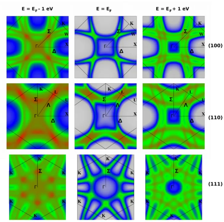
FIG. 6. Map of the Bloch Spectral Function calculated with the code SPRKKR for three different planes of the first BZ of Ge2.005Sb2Te5: (100) in upper-row panels, (110) in middle-row panels, and (111) in lower-row panels, and for each of them at
three different energies: (EF− 1 eV) on the left side, EF in the middle, and (EF+ 1 eV) on the right side. The color coding
is the same as in fig. 4.
gap) will be located at the L-points, at the W-points, between Γ and X-points, and between Γ and K-points.
For a given wave vector, the strong Lorentzian broadening of the electron states shown in figure 4 is inversely proportional to their lifetime τ , and therefore, directly proportional to the imaginary part of the energy.94,107,108 This broadening strongly depends on the disorder rate on atomic sites A, as it can be seen
in figure 5, where we compare the BSF of Ge1.5Sb2Te5
(in this case the Fermi level is in the valence band) and of Ge2.5Sb2Te5 (for which EF crosses the conduction
band): the reminiscence of the band structure of an ordered crystal is much more clear for the latter. This is due to the fact that vacancies on atomic sites A are a more important cause of electron-state broadening than the statistical disorder between Ge and Sb atoms. We can also notice in this figure that the broadening depends
on the energy E, and on the wave vector k. Chemical disorder does not actually suppress the band gap near EF at the L-point of the first BZ: the broadening of
electron states on both sides of this band gap gives the impression that the band gap vanishes, in particular at higher vacancy-concentration. However, these states remain clearly split (giving rise to the band gap), and the energy difference between them (i. e. the energy width of the band gap) does not seem to decrease when the chemical disorder increases, and thus, does not lead to the suppression of the band gap. The stoichiometry modifies the broadening of electron states on both sides of the band gap, without changing their energy splitting.
Map of the electron states in the first Brillouin zone: Figure 6 shows a plot of the BSF AB(E, k) for
k belonging to three different planes in the first BZ of Ge2.005Sb2Te5 and for three different energies. The
three upper panels show the BSF map in the (100) BZ plane containing two perpendicular 4 directions (Γ-X-W-K plane), the middle panels show similar plots for the (110) BZ plane containing 4, Σ, and Λ directions (Γ-X-U-L plane), and the lower panels show similar plots for the (111) plane containing six Σ directions (Γ-K). The left side, central, and right side columns respectively correspond to the energies (EF − 1 eV),
EF, and (EF + 1 eV). The color coding is exactly
the same as in figure 4. Figure 6 helps to perform deeper inspections of the k-resolved states as compared to figure 4, which only focuses on the high-symmetry directions of the BZ: it confirms that the main valleys occupied by conduction electrons of this metallic Ge-rich GST compound are mostly located at the L points, and between Γ and K points on the Σ directions. Figure 6 also gives additional information on the anisotropy of these valleys, and on the disorder induced broadening of the electron states, which is proportional to their lifetime τ (k, E). The figure shows that the Lorentzian broadening actually depends on wave vector and energy. This is a major constraint for calculating accurately the conductivity of a disordered system using the semi-classical Boltzman transport equation, where τ is generally considered as identical for all the states.89,109
The results presented in figures 4, 5, and 6 can be very useful for experimentalists who measure the disper-sion of electron states in GST crystals with photoemis-sion or inverse photoemisphotoemis-sion techniques. Angle resolved photoemission spectroscopy (ARPES) has, for instance, been recently used to measure the dispersion of the oc-cupied electron states in samples of cubic metastable Ge2Sb2Te5.39 Our results shown in figure 6 for the (111)
cut of the first BZ near EF resemble the ARPES
mea-surements presented by these authors.
FIG. 7. Electrical conductivity of Ge2+xSb2Te5 (in red) and
Ge2Sb2+yTe5(in blue) GST compounds, as a function of the
Ge or Sb concentration.
C. Electrical conductivity versus Ge or Sb content
The dc conductivity σ of the Ge2+xSb2Te5 and
Ge2Sb2+yTe5 crystals is represented in figure 7 as a
function of the composition for Ge-rich or deficient (red lines) and Sb-rich or deficient (blue lines) compounds. These results have been calculated with the code SPRKKR, using the lattice parameters computed with VASP for the same compositions. These values of the conductivity, which all fall in the range of 105 – 106
[Ω · m]−1, have been calculated from ground-state DFT calculations and would correspond to the temperature 0 K. The values of the conductivity that we calculated for off-stoichiometric GST crystals are of the same order of magnitude as those measured for GST crystals in experiments.110–112 They are however higher than those
measured in experiments. This is not surprising for the two following reasons: firstly, the conductivity has been measured for GST compositions closer to that of Ge2Sb2Te5 (i.e. for crystals with a lower densities
of charge carriers than in the off-stoichiometric and doped GST crystals that we considered); secondly, we calculated the electrical conductivity at T=0 K, while experimental values have been measured at finite temperature (electrons being scattered by phonons, the conductivity of a metal decreases when the temperature increases).
The conductivity has not been explicitly calculated for Ge2Sb2Te5 (x = 0 and y = 0): at the temperature 0
K, this compound being a semiconductor, its conduc-tivity would vanish. As soon as the composition devi-ates from the stoichiometry of Ge2Sb2Te5, the crystal
becomes metallic and its conductivity increases. The modification of the conductivity of the GST crystals is due, on the one hand, to changes in the density of the charge carriers, and on the other hand, to modifications of the chemical disorder that scatters the electrons with
an energy near the Fermi level. The density of charge carriers increases with the deviation from the 225 sto-ichiometry. This increase holds for both x (or y) > 0 (electrons populate the conduction band), and x (or y) < 0 (holes populate the valence band). This tends to increase the conductivity. However, the scattering of the charge carriers by disorder on the atomic site A is higher when there are more vacancies in the crystal, i.e. for Ge-or Sb-poGe-or GST compounds, x (Ge-or y) < 0. This higher disorder-induced scattering of the charge carriers tends to increase the resistivity of the crystal, thus making Ge-or Sb-poGe-or GST compounds less conductive as compared to Ge- or Sb-rich GST compounds, for the same density of charge carriers (i.e., for the same |x| or |y|). The con-ductivity of GST compounds is always higher when Sb atoms have been added to the crystal (or removed) than when the same quantity of Ge atoms have been added (or removed). This is due to the fact that the variations of the number of valence electrons is higher in the for-mer than in the latter case: the electronic structure of an isolated Sb atom is [Kr]4d105s25p3, while that of an
isolated Ge atom is [Ar]3d104s24p2.
V. EFFECTS OF Si DOPING
FIG. 8. Total DOS and contribution of each chemical species for Ge1.7Sb2Si0.2Te5 (upper panel) and Ge1.7Sb2Si0.4Te5
(lower panel).
In this section, we describe the electronic properties of the GST crystals Ge2+xSb2Te5, doped with Si atoms.
With an electronic structure given by [Ne]3s23p2,
isolated Si atoms possess the same number of s and p valence electrons as Ge atoms. We first calculated the lattice parameter of Si-doped GST compounds, using the code VASP and the same supercells as those used to study Ge2+xSb2Te5, in which some of the vacant sites
have been gradually filled with Si atoms: the calculated lattice parameter (not shown here) increases slightly with the number of Si atoms. It increases, for instance, by 0.3% only between Ge1.9Sb2Te5and Ge1.9Sb2Si0.6Te5.
FIG. 9. Contribution of single Ge, Sb, and Si atoms to the DOS of Ge1.7Sb2Te5 crystals doped with different
concentra-tions of Si atoms. The s and p partial DOS curves are also shown. Upper and lower panels respectively correspond to Ge1.7Sb2Si0.2Te5 and Ge1.7Sb2Si0.4Te5.
Figure 8 shows the DOS curves calculated for the GST compound Ge1.7Sb2SizTe5doped with two different
con-centrations of Si atoms: z = 0.2, for which the Fermi level is below the band gap, and z = 0.4, for which it is above it. The doped GST crystals behave like metals for these two compositions. The contribution of the dif-ferent chemical species is also shown in the figure. The contributions of Ge, Te, and Sb do not strongly change with the concentration of Si atoms. Of course, the con-tribution of Si is higher for Ge1.7Sb2Si0.4Te5 than for
Ge1.7Sb2Si0.2Te5. Figure 9 shows the total and s- and
p-partial DOS per Ge, Sb and Si atom, for the same Si-doped GST crystals as in figure 8. For both crystals, the partial DOS curves are very similar for Si and Ge atoms, with electron bands in exactly the same energy ranges: replacing vacancies by Si instead of Ge atoms does not strongly change the nature of the electron states. We also note in this figure that, whatever the density of Si dopant atoms is, electron states mostly involve p atomic orbitals of Ge, Sb, and Si atoms at energies in the vicinity of the band gap.
The BSF of Ge2+xSb2SizTe5 (not shown here) is very
similar to that of Ge2+x+zSb2Te5, which confirms that
replacing Ge by Si atoms does not strongly increase the broadening of the electron states, despite the additional chemical disorder induced by this substitution.
FIG. 10. Electrical conductivity of Ge2+xSb2SizTe5
com-pounds calculated for x = -0.1 (in brown), x = 0.0 (in black), and x = 0.1 (in green) versus concentration of dopant Si atoms.
Figure 10 shows the electrical conductivity of three dif-ferent Ge2+xSb2SizTe5 crystals (x = -0.1, 0.0, and 0.1)
as a function of the concentration of dopant Si atoms. The variations of the conductivity as a function of dop-ing depend on the value of x. If x <0 (brown curve), the conductivity first decreases with z up to the critical concentration at which the crystal becomes a semicon-ductor (σ = 0 at T = 0 K), before increasing again when electrons from additional dopant atoms start populat-ing the conduction band above the band gap. If x = 0 (black curve), the undoped crystal is a semiconductor and starts behaving like a metal when dopant atoms are added, which increases the conductivity. If x >0 (green curve), even the undoped crystal is a metal, and doping increases the occupation of the conduction band and the conductivity.
VI. DISCUSSION
In the previous sections, we have described the mod-ifications of the dc conductivity with the concentration of Ge, Sb, or dopant Si atoms in GST crystals near the 225 stoichiometry. We have considered different situations, which all belong to the same general formula Ge2+xSb2+ySizTe5: the x-, y-, and z-dependences of
the conductivity displayed in figures 7 and 10 look very different, and the values shown in these figures strongly depend on the chemical species, the concentration of which is changed with respect to that of Ge2Sb2Te5.
We now present an overall discussion of these results in terms of the concentration of charge carriers and of the electron scattering induced by chemical disorder in the GST crystal.
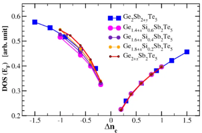
Figure 11 shows exactly the same conductivity values as in figures 7 and 10, but plotted as a function of 4ne,
the variation of the number of valence electrons per
for-FIG. 11. Conductivity of Ge2+xSb2+ySizTe5 crystals as a
function of 4ne, the difference in their number of p-valence
electrons per formula unit with respect to Ge2Sb2Te5.
FIG. 12. Top: electrical conductivity of Ge2+x−zSb2SizTe5
crystals for z = 0.0 (red), 0.2 (orange), 0.4 (violet), and 0.6 (magenta), as a function of 4ne. Bottom: for the same
sys-tems, difference between these conductivities and the conduc-tivity of Ge2+xSb2Te5.
mula unit, due to the deviation from the 225 stoichiom-etry and due to Si-doping, in the Ge2Sb2Te5 crystal. In
other words, 4neis given by
4ne= ne(Ge2+xSb2+ySizTe5) − ne(Ge2Sb2Te5). (4)
elec-trons of Ge, Sb, and Si atoms to evaluate 4ne, since the
electron states near EF that become occupied or
unoccu-pied when x, y and z vary, mostly involve the p-orbitals of these atoms, as shown in figure 9. 4neis then given
by
4ne= 2x + 3y + 2z. (5)
Figure 11 shows that all the values of the conductivity that we have calculated for different GST crystals, more or less belong to the same curve when plotted as a func-tion of 4ne. However, non-negligible differences can be
observed in figure 11, between the conductivities of GST crystals possessing the same number of p-valence elec-trons (same value of 4ne) but different compositions.
This is clearly visible from the comparison of the two curves describing the conductivity of Ge2+xSb2Te5(red)
and Ge2Sb2+yTe5(blue) crystals versus 4ne< 0. These
differences are due to the differences of chemical disor-der in these crystals. To emphasize this last point, we have calculated the conductivity of three different fam-ilies of Si-doped GST compounds: Ge1.4+xSb2Si0.6Te5,
Ge1.6+xSb2Si0.4Te5, and Ge1.8+xSb2Si0.2Te5, which
ex-actly correspond to the same values of 4ne = 2x, and
to the same concentrations of vacancies on site A. The values of the conductivity of these three families of Si-doped GST crystals are represented in the upper panel of figure 12 as a function of 4ne. The values of the
con-ductivity for the undoped Ge2+xSb2Te5 crystals are also
shown in this figure for reference. The differences 4σ = σ(Ge2+x−zSb2SizTe5) − σ(Ge2+xSb2Te5) (6)
between the conductivities of the Si-doped and undoped GST crystals are shown in the lower panel of figure 12. These differences are only due to the excess of chemical disorder resulting from the substitution of Ge by Si atoms in the crystals. They are more important for 4ne> 0, than for 4ne < 0. However, the conductivity
differences between crystals with the same concentration of valence electrons and the same number of vacancies on atomic sites A are smaller than those between GST crystals with the same number of valence electrons but different concentrations of vacancies (compare, for instance, the conductivity curves of Ge-poor and Sb-poor crystals for the same values of 4nein figure 11)
Although figures 11 and 12 have shown that the con-ductivity of off-stoichiometric or Si-doped GST crystals depend both on the number of valence electrons and on the chemical disorder rate (in particular, the concentra-tion of vacancies in the crystal), this dependence is not easy to analyze. We can, for instance, compare the val-ues of the conductivity with those of the DOS at the Fermi level, represented in figure 13 as a function of 4ne
for the same crystals as in figures 7 and 12. This com-parison shows that σ and the DOS at EF behave quite
similarly with 4ne. However, σ is not only determined
by the DOS at EF: the nature and rate of the chemical
FIG. 13. Density of electron states at EF as a
func-tion of 4ne for Ge2+x−zSb2SizTe5 crystals with z = 0.0
(red), 0.2 (orange), 0.4 (violet), and 0.6 (magenta), and for Ge2Sb2+ySizTe5crystals (blue).
disorder responsible for electron scattering also play sig-nificant role. This has been shown in former theoretical investigations on the conductivity of alloys with random disorder.94,113,114
VII. CONCLUSION
We have presented a numerical study of the electronic structure and conductivity of pure and Si-doped GST crystals, with the rock-salt structure and a stoichiometry close to that of Ge2Sb2Te5. The numerical calculations
have been performed with the first-principles code SPRKKR, which uses the KKR-CPA method, based on the multiple-scattering theory and on a description of the random disorder among Ge, Sb, Si (dopant) atoms, and vacancies in the crystal through the coherent po-tential approximation. The accuracy of this method for studying off-stoichiometric and doped GST crystals has been verified, by comparing the DOS curves calculated with this method and with a Kohn-Sham wavefunc-tion based method using supercell in the code VASP. Although KKR-CPA does not take distortions of the rock-salt structure into account, this comparison shows that the DOS curves calculated with the code SPRKKR remarkably agree with their VASP counterparts: this validates the applicability of the KKR-CPA method, with a reasonable accuracy for calculating electronic properties of off-stoichiometric and doped GST crystals. In comparison with Kohn-Sham wave function based methods, the KKR-CPA method is advantageous as it takes less time and less computational resources.
The KKR-CPA method has been applied to Ge-or Sb-rich Ge-or deficient GST crystals (with respect to Ge2Sb2Te5), which all present a metallic behavior. We
have used this method to calculate the Bloch spectral function and the zero-temperature dc electrical
conduc-tivity. The calculated Bloch spectral function has given a clear information on the valleys that will be occupied by charge carriers in these crystals as a function of their composition. The Fermi level is shifted below the band gap for Ge- or Sb-poor GST compounds, and it has been shown that the broadening of the electron states increases in this case with the concentration of vacancies. This broadening is lowered for Ge- or Sb-rich compounds (EF above the band gap). We
have given values for the zero-temperature dc electrical conductivity of the off-stoichiometric GST compounds (Ge2+xSb2Te5 and Ge2Sb2+yTe5), and shown that it
increases with deviations from the 225 stoichiometry, in particular for Ge- or Sb-rich crystals. We have also described the electronic properties of Si-doped GST compounds and calculated their conductivity. It has been shown that doping with Si atoms has similar effects on the electron states, their broadening, and the conductivity as increasing the concentration of Ge atoms in the crystal. However, Si-doping slightly modifies the conductivity since it increases the chemical disorder.
We have finally shown that the calculated conductiv-ity mostly depends on the overall densconductiv-ity of valence p-electrons in the GST crystal, which results both from off-stoichiometry and doping. However, the conductivity
also depends on the intrinsic chemical disorder due to random distribution of Ge, Sb, Si atoms and vacancies. We have shown that, increasing the vacancy concentra-tion has a bigger impact on the conductivity than replac-ing Ge by Si atoms for the same density of valence elec-trons. These results, although calculated using a mean-field description of the chemical disorder, show the effects of the chemical composition on the zero-temperature con-ductivity of GST crystals. We believe that they will be useful in modelling GST samples, with micro-metric grains having compositions close to that of Ge2Sb2Te5.
ACKNOWLEDGMENTS
This work was granted access to the HPC resources of CALMIP supercomputing center under the alloca-tion p17025 (2017-2019). This work has been supported through the grant NEXT n◦ ANR-10-LABX-0037 in the framework of the “Programme des Investissements d’Avenir”. It was also partly funded by Minefi under the Nano 2017 Program. We also acknowledge insight-ful discussions with Daniel Benoit at STMicroelectron-ics, Crolles and with Alain Claverie at CEMES, CNRS, Toulouse for having driven our attention to the differ-ent technological challenges and aspects from material science perspective.
∗
rajarshi.sinharoy@cemes.fr, lionel.calmels@cemes.fr
1 S. R. Ovshinsky, Phys. Rev. Lett. 21, 1450 (1968). 2 G. W. Burr, R. M. Shelby, A. Sebastian, S. Kim,
S. Kim, S. Sidler, K. Virwani, M. Ishii, P. Narayanan, A. Fumarola, L. L. Sanches, I. Boybat, M. L. Gallo, K. Moon, J. Woo, H. Hwang, and Y. Leblebici, Advances in Physics: X 2, 89 (2017), https://doi.org/10.1080/23746149.2016.1259585.
3 P. No´e, C. Valle, F. Hippert, F. Fillot, and J.-Y.
Raty, Semiconductor Science and Technology 33, 013002 (2018).
4 N. Yamada, E. Ohno, K. Nishiuchi, N. Akahira,
and M. Takao, J. Appl. Phys. 69, 2849 (1991), https://doi.org/10.1063/1.348620.
5 D. Lencer, M. Salinga, B. Grabowski, T. Hickel, J.
Neuge-bauer, and M. Wuttig, Nature Materials 7, 972 EP (2008), article.
6 M. H. R. Lankhorst, B. W. S. M. M. Ketelaars, and
R. A. M. Wolters, Nature Materials 4, 347 EP (2005), article.
7
M. Wuttig and N. Yamada, Nature Materials 6, 824 EP (2007), review Article.
8
N. Yamada, MRS Bulletin 21, 4850 (1996).
9
T. Matsunaga, R. Kojima, N. Yamada, K. Ki-fune, Y. Kubota, Y. Tabata, and M. Takata, Inorg. Chem. 45, 2235 (2006), PMID: 16499389, https://doi.org/10.1021/ic051677w.
10 M. Wuttig, D. L¨usebrink, D. Wamwangi, W. Welnic,
M. Gilleßen, and R. Dronskowski, Nature Materials 6, 122 EP (2006), article.
11
J. L. F. Da Silva, A. Walsh, and H. Lee, Phys. Rev. B 78, 224111 (2008).
12 B. Sa, J. Zhou, Z. Song, Z. Sun, and R. Ahuja, Phys.
Rev. B 84, 085130 (2011).
13
B. Sa, J. Zhou, Z. Sun, J. Tominaga, and R. Ahuja, Phys. Rev. Lett. 109, 096802 (2012).
14
E. Morales-S´anchez, E. F. Prokhorov, A. Mendoza-Galv´an, and J. Gonz´alez-Hern´andez, J. Appl. Phys. 91, 697 (2002), https://doi.org/10.1063/1.1427146.
15
T. Nonaka, G. Ohbayashi, Y. Toriumi, Y. Mori, and H. Hashimoto, Thin Solid Films 370, 258 (2000).
16 T. Matsunaga, N. Yamada, and Y. Kubota, Acta
Crys-tallographica Section B 60, 685 (2004).
17
A. Lotnyk, S. Berntz, X. Sun, U. Ross, M. Ehrhardt, and B. Rauschenbach, Acta Materialia 105, 1 (2016).
18 B. Zhang, W. Zhang, Z. Shen, Y. Chen, J. Li,
S. Zhang, Z. Zhang, M. Wuttig, R. Mazzarello, E. Ma, and X. Han, Appl. Phys. Lett. 108, 191902 (2016), https://doi.org/10.1063/1.4949011.
19
V. Bragaglia, F. Arciprete, W. Zhang, A. M. Mio, E. Za-llo, K. Perumal, A. Giussani, S. Cecchi, J. E. Boschker, H. Riechert, S. Privitera, E. Rimini, R. Mazzarello, and R. Calarco, Scientific Reports 6, 23843 EP (2016), article.
20
S. He, L. Zhu, J. Zhou, and Z. Sun, In-org. Chem. 56, 11990 (2017), PMID: 28933542, https://doi.org/10.1021/acs.inorgchem.7b01970.
21
I. Hilmi, A. Lotnyk, J. W. Gerlach, P. Schumacher, and B. Rauschenbach, Materials & Design 115, 138 (2017).
22
Z. Sun, J. Zhou, and R. Ahuja, Phys. Rev. Lett. 96, 055507 (2006).
23
X. Q. Liu, X. B. Li, L. Zhang, Y. Q. Cheng, Z. G. Yan, M. Xu, X. D. Han, S. B. Zhang, Z. Zhang, and E. Ma, Phys. Rev. Lett. 106, 025501 (2011).
24
J.-Y. Raty, C. Bichara, R. Mazzarello, P. Rausch, P. Zalden, and M. Wuttig, Phys. Rev. Lett. 108, 239601 (2012).
25
P. Fons, A. V. Kolobov, J. Tominaga, S. Kohara, M. Takata, T. Matsunaga, N. Yamada, and S. Bokoch, Phys. Rev. Lett. 108, 239603 (2012).
26
J. Kalikka, J. Akola, J. Larrucea, and R. O. Jones, Phys. Rev. B 86, 144113 (2012).
27 I. Ronneberger, W. Zhang, H. Eshet, and R. Mazzarello,
Advanced Functional Materials 25, 6407 (2015).
28
J. Kalikka, J. Akola, and R. O. Jones, Phys. Rev. B 94, 134105 (2016).
29
W. K. Njoroge, H.-W. Wltgens, and M. Wut-tig, J. Vac. Sci. Technol. A 20, 230 (2002), https://doi.org/10.1116/1.1430249.
30 I. I. Petrov, R. M. Iamov, and Z. G. Pinsker, Sov. Phys.
Crystallogr. 13, 339 (1968).
31
B. J. Kooi and J. T. M. De Hosson, J. Appl. Phys. 92, 3584 (2002), https://doi.org/10.1063/1.1502915.
32
K. Shportko, S. Kremers, M. Woda, D. Lencer, J. Robert-son, and M. Wuttig, Nature Materials 7, 653 EP (2008), article.
33
T. Kato and K. Tanaka, Jpn. J. Appl. Phys. 44, 7340 (2005).
34 S. Lee, J. R. Abelson, S. G. Bishop, D.-H. Kang,
B.-k. Cheong, and K.-B. Kim, J. Appl. Phys. 97, 093509 (2005), https://doi.org/10.1063/1.1884248.
35 J. Akola and R. O. Jones, Phys. Rev. B 76, 235201 (2007). 36 S. Caravati, M. Bernasconi, T. D. Khne, M. Krack, and
M. Parrinello, Journal of Physics: Condensed Matter 21, 255501 (2009).
37 J. Akola and R. O. Jones, Phys. Status Solidi B 249, 1851
(2012).
38
C. Pauly, M. Liebmann, A. Giussani, J. Kellner, S. Just, J. Snchez-Barriga, E. Rienks, O. Rader, R. Calarco, G. Bihlmayer, and M. Morgenstern, Appl. Phys. Lett. 103, 243109 (2013), https://doi.org/10.1063/1.4847715.
39 J. Kellner, G. Bihlmayer, M. Liebmann, S. Otto,
C. Pauly, J. E. Boschker, V. Bragaglia, S. Cecchi, R. N. Wang, V. L. Deringer, P. K¨uppers, P. Bhaskar, E. Go-lias, J. S´anchez-Barriga, R. Dronskowski, T. Fauster, O. Rader, R. Calarco, and M. Morgenstern, Commu-nications Physics 1, 5 (2018).
40
M. Agati, F. Renaud, D. Benoit, and A. Claverie, MRS Commun. 8, 11451152 (2018).
41
S. Privitera, E. Rimini, C. Bongiorno, R. Zonca, A. Pirovano, and R. Bez, J. Appl. Phys. 94, 4409 (2003), https://doi.org/10.1063/1.1604458.
42
G. Navarro, M. Cou, A. Kiouseloglou, P. No´e, F. Fillot, V. Delaye, A. Persico, A. Roule, M. Bernard, C. Sab-bione, D. Blachier, V. Sousa, L. Perniola, S. Maitre-jean, A. Cabrini, G. Torelli, P. Zuliani, R. Annunzi-ata, E. Palumbo, M. Borghi, G. Reimbold, and B. D. Salvo, 2013 IEEE International Electron Devices Meet-ing, ISSN 2156-017X, 21.5.1 (2013).
43
P. Zuliani, E. Varesi, E. Palumbo, M. Borghi, I. Tortorelli, D. Erbetta, G. D. Libera, N. Pessina, A. Gandolfo, C. Pre-lini, L. Ravazzi, and R. Annunziata, IEEE Transactions on Electron Devices 60, 4020 (2013).
44
N. Yamada and T. Matsunaga, J. Appl. Phys. 88, 7020 (2000), https://doi.org/10.1063/1.1314323.
45
K.-J. Choi, S.-M. Yoon, N.-Y. Lee, S.-Y. Lee, Y.-S. Park, B.-G. Yu, and S.-O. Ryu, Thin Solid Films 516, 8810 (2008).
46
S.-M. Yoon, K.-J. Choi, N.-Y. Lee, S.-Y. Lee, Y.-S. Park, and B.-G. Yu, Jpn. J. Appl. Phys. 46, 7225 (2007).
47 T.-Y. Yang, I.-M. Park, H.-Y. You, S.-H. Oh, K.-W. Yi,
and Y.-C. Joo, J. Electrochem. Soc. 156, H617 (2009), http://jes.ecsdl.org/content/156/8/H617.full.pdf+html.
48 S. Privitera, C. Bongiorno, E. Rimini, and
R. Zonca, Appl. Phys. Lett. 84, 4448 (2004), https://doi.org/10.1063/1.1759063.
49 Y. Lai, B. Qiao, J. Feng, Y. Ling, L. Lai, Y. Lin, T. Tang,
B. Cai, and B. Chen, Journal of Electronic Materials 34, 176 (2005).
50 Y. Kim, K. Jeong, M.-H. Cho, U. Hwang, H. S. Jeong,
and K. Kim, Appl. Phys. Lett. 90, 171920 (2007), https://doi.org/10.1063/1.2722203.
51 M.-C. Jung, Y. M. Lee, H.-D. Kim, M. G. Kim, H. J.
Shin, K. H. Kim, S. A. Song, H. S. Jeong, C. H. Ko, and M. Han, Appl. Phys. Lett. 91, 083514 (2007), https://doi.org/10.1063/1.2773959.
52 R. M. Shelby and S. Raoux, J. Appl. Phys. 105, 104902
(2009), https://doi.org/10.1063/1.3126501.
53
E. Cho, S. Han, D. Kim, H. Horii, and H.-S. Nam, J. Appl. Phys. 109, 043705 (2011), https://doi.org/10.1063/1.3553851.
54
K. Kim, J.-C. Park, J.-G. Chung, S. A. Song, M.-C. Jung, Y. M. Lee, H.-J. Shin, B. Kuh, Y. Ha, and J.-S. Noh, Appl. Phys. Lett. 89, 243520 (2006), https://doi.org/10.1063/1.2408660.
55 S.-J. Kim, J.-H. Choi, S.-C. Lee, B.-k. Cheong, D. S.
Jeong, and C. Park, J. Appl. Phys. 107, 103522 (2010), https://doi.org/10.1063/1.3428362.
56
S. Caravati, D. Colleoni, R. Mazzarello, T. D. Khne, M. Krack, M. Bernasconi, and M. Parrinello, Journal of Physics: Condensed Matter 23, 265801 (2011).
57
T. H. Jeong, M. R. Kim, H. Seo, J. W. Park, and C. Yeon, Jpn. J. Appl. Phys. 39, 2775 (2000).
58
H. Seo, T.-H. Jeong, J.-W. Park, C. Yeon, S.-J. Kim, and S.-Y. Kim, Jpn. J. Appl. Phys. 39, 745 (2000).
59 E. M. Vinod, K. Ramesh, and K. S. Sangunni, Scientific
Reports 5, 8050 EP (2015), article.
60
C. Koch, A.-L. Hansen, T. Dankwort, G. Schienke, M. Paulsen, D. Meyer, M. Wimmer, M. Wuttig, L. Kienle, and W. Bensch, RSC Adv. 7, 17164 (2017).
61
T.-J. Park, S.-Y. Choi, and M.-J. Kang, Thin Solid Films 515, 5049 (2007), the Third International Symposium on Dry Process (DPS 2005).
62
P. Lazarenko, P. Nguyen, H., S. Kozyukhin, and A. Sherchenkov, 13, 1400 (2011).
63 A. Sherchenkov, S. Kozyukhin, A. Babich, and
P. Lazarenko, J. Non-Cryst. Solids 377, 26 (2013), iSNOG 2012 Proceedings of the 18th International Sym-posium on Non-Oxide and New Optical Glasses Rennes, France, July 1-5, 2012.
64
P. I. Lazarenko, A. A. Sherchenkov, S. S. Kozyukhin, M. Y. Shtern, S. P. Timoshenkov, D. G. Gromov, and E. N. Redichev, Proc.SPIE 9440, 9440 (2014).
65
S. Kozyukhin, A. Sherchenkov, A. Babich, P. Lazarenko, H. P. Nguyen, and O. Prikhodko, Can. J. Phys. 92, 684 (2014), https://doi.org/10.1139/cjp-2013-0607.
66
K. Wang, C. Steimer, D. Wamwangi, S. Ziegler, M. Wut-tig, J. Tomforde, and W. Bensch, Microsystem Technolo-gies 13, 203 (2007).
67
S. Kozyukhin, M. Veres, H. Nguyen, A. Ingram, and V. Kudoyarova, Physics Procedia 44, 82 (2013), 10th International Conference on Solid State Chemistry, Par-dubice, Czech Republic.
68 J. M. Skelton, A. R. Pallipurath, T.-H. Lee, and S. R.
Elliott, Advanced Functional Materials 24, 7291 (2014).
69
X. Cheng, L. Bo, S. Zhi-Tang, F. Song-Lin, and C. Bomy, Chinese Physics Letters 22, 2929-2932 (2005).
70 K. Wang, D. Wamwangi, S. Ziegler, C. Steimer, M. J.
Kang, S. Y. Choi, and M. Wuttig, Phys. Status Solidi A 201, 3045 (2004).
71 T. J. Park, D. H. Kim, S. M. Yoon, K. J. Choi, N. Y. Lee,
B. G. Yu, and S. Y. Choi, Jpn. J. Appl. Phys. 45, L1273 (2006).
72 M. L. Lee, K. T. Yong, C. L. Gan, L. H. Ting, S. B. M.
Daud, and L. P. Shi, J. Phys. D 41, 215402 (2008).
73
J. Zhou, Z. Sun, L. Xu, and R. Ahuja, Solid State Com-mun. 148, 113 (2008).
74 G. Singh, A. Kaura, M. Mukul, and S. K. Tripathi,
Jour-nal of Materials Science 48, 299 (2013).
75
N. Bai, F. Liu, X. Han, Z. Zhu, F. Liu, X. Lin, and N. Sun, Applied Surface Science 316, 202 (2014).
76
S. Welzmiller, T. Rosenthal, P. Ganter, L. Neudert, F. Fahrnbauer, P. Urban, C. Stiewe, J. de Boor, and O. Oeckler, Dalton Trans. 43, 10529 (2014).
77
B. Qiao, J. Feng, Y. Lai, Y. Ling, Y. Lin, T. Tang, B. Cai, and B. Chen, Applied Surface Science 252, 8404 (2006).
78 Q. Bao-Wei, F. Jie, L. Yun-Feng, L. Yun, L. Yin-Yin,
T. Ting-Ao, C. Bing-Chu, and C. Bomy, Chinese Physics Letters 23, 172 (2006).
79 Y. Ling, Y. Lin, B. Qiao, Y. Lai, J. Feng, T. Tang, B. Cai,
and B. Chen, Jpn. J. Appl. Phys. 45, L349 (2006).
80
J. Feng, Y. Zhang, B. Qiao, Y. Lai, Y. Lin, B. Cai, T. Tang, and B. Chen, Applied Physics A 87, 57 (2007).
81 T. Zhang, Z. Song, B. Liu, S. Feng, and B. Chen,
Solid-State Electronics 51, 950 (2007).
82
T. Zhang, Z. Song, F. Rao, G. Feng, B. Liu, S. Feng, and B. Chen, Jpn. J. Appl. Phys. 46, L247 (2007).
83
S.-J. Park, I.-S. Kim, S.-K. Kim, S.-M. Yoon, B.-G. Yu, and S.-Y. Choi, Semiconductor Science and Technology 23, 105006 (2008).
84
S.-M. Jeong, K.-H. Kim, S.-M. Choi, and H.-L. Lee, Jpn. J. Appl. Phys. 48, 045503 (2009).
85 Y. Jiang, L. Xu, J. Chen, R. Zhang, W. Su, Y. Yu, Z. Ma,
and J. Xu, Phys. Status Solidi A 210, 2231 (2013).
86
H. Ebert and et al., The Munich SPR-KKR package (ver-sion 6.3) http://ebert.cup.uni-muenchen.de/sprkkr.
87 H. Ebert, D. Kdderitzsch, and J. Minr, Rep. Prog. Phys.
74, 096501 (2011).
88
P. Soven, Phys. Rev. 156, 809 (1967).
89 G. K. Madsen and D. J. Singh, Comput. Phys. Commun.
175, 67 (2006).
90
J. S. Faulkner and G. M. Stocks, Phys. Rev. B 21, 3222 (1980).
91 H. Ebert, A. Vernes, and J. Banhart, Solid State
Com-mun. 104, 243 (1997).
92 R. Kubo, J. Phys. Soc. Jpn. 12, 570 (1957),
https://doi.org/10.1143/JPSJ.12.570.
93
D. A. Greenwood, Proc. Phys. Soc. 71, 585 (1958).
94
W. H. Butler, Phys. Rev. B 31, 3260 (1985).
95 B. Velick´y, Phys. Rev. 184, 614 (1969). 96
J. P. Perdew, K. Burke, and M. Ernzerhof, Phys. Rev. Lett. 77, 3865 (1996).
97 J. P. Perdew, K. Burke, and M. Ernzerhof, Phys. Rev.
Lett. 78, 1396 (1997).
98
G. Kresse and J. Hafner, Phys. Rev. B 47, 558 (1993).
99 G. Kresse and D. Joubert, Phys. Rev. B 59, 1758 (1999). 100
J. P. Perdew, A. Ruzsinszky, G. I. Csonka, O. A. Vydrov, G. E. Scuseria, L. A. Constantin, X. Zhou, and K. Burke, Phys. Rev. Lett. 100, 136406 (2008).
101 J. P. Perdew, A. Ruzsinszky, G. I. Csonka, O. A. Vydrov,
G. E. Scuseria, L. A. Constantin, X. Zhou, and K. Burke, Phys. Rev. Lett. 102, 039902 (2009).
102 G. I. Csonka, J. P. Perdew, A. Ruzsinszky, P. H. T.
Philipsen, S. Leb`egue, J. Paier, O. A. Vydrov, and J. G. ´
Angy´an, Phys. Rev. B 79, 155107 (2009).
103 F. Tran and P. Blaha, Phys. Rev. Lett. 102, 226401
(2009).
104
L. Hedin, Phys. Rev. 139, A796 (1965).
105 V. I. Anisimov, F. Aryasetiawan, and A. I. Lichtenstein,
Journal of Physics: Condensed Matter 9, 767 (1997).
106
S. ichi Shamoto, K. Kodama, S. Iikubo, T. Taguchi, N. Yamada, and T. Proffen, Jpn. J. Appl. Phys. 45, 8789 (2006).
107
B. E. A. Gordon, W. E. Temmerman, and B. L. Gyorffy, J. Phys. F 11, 821 (1981).
108 B. Wiendlocha, Phys. Rev. B 88, 205205 (2013). 109
W. Yu, V. Mauchamp, T. Cabioch, D. Magne, L. Gence, L. Piraux, V. Gauthier-Brunet, and S. Dubois, Acta Ma-terialia 80, 421 (2014).
110
R. Fallica, J.-L. Battaglia, S. Cocco, C. Monguzzi, A. Teren, C. Wiemer, E. Varesi, R. Cecchini, A. Gotti, and M. Fanciulli, Journal of Chemical & Engineering Data 54, 1698 (2009), https://doi.org/10.1021/je800770s.
111
W. K. Njoroge, H.-W. W¨oltgens, and M. Wut-tig, J. Vac. Sci. Technol. A 20, 230 (2002), https://doi.org/10.1116/1.1430249.
112
I. Friedrich, V. Weidenhof, W. Njoroge, P. Franz, and M. Wuttig, J. Appl. Phys. 87, 4130 (2000), https://doi.org/10.1063/1.373041.
113
A.-B. Chen, G. Weisz, and A. Sher, Phys. Rev. B 5, 2897 (1972).
114 W. H. Butler and G. M. Stocks, Phys. Rev. B 29, 4217
![FIG. 1. Top: 300 atomic site supercell relaxed with the code VASP. The c direction corresponds to the [111] axis of the rock-salt Ge 2 Sb 2 Te 5 crystal, along which layers of Te (yellow) and of Ge (purple) and Sb (orange sphere) atoms are alterna-tively](https://thumb-eu.123doks.com/thumbv2/123doknet/13758062.438152/4.918.484.833.76.457/atomic-supercell-relaxed-direction-corresponds-crystal-layers-alterna.webp)