HAL Id: hal-02997616
https://hal.uca.fr/hal-02997616
Submitted on 10 Nov 2020
HAL is a multi-disciplinary open access
archive for the deposit and dissemination of sci-entific research documents, whether they are pub-lished or not. The documents may come from teaching and research institutions in France or abroad, or from public or private research centers.
L’archive ouverte pluridisciplinaire HAL, est destinée au dépôt et à la diffusion de documents scientifiques de niveau recherche, publiés ou non, émanant des établissements d’enseignement et de recherche français ou étrangers, des laboratoires publics ou privés.
Optical and structural analysis of ultra-long GaAs
nanowires after nitrogen-plasma passivation
Yamina André, Nebile Isik Goktas, Guillaume Monier, Hadi Hijazi, Hussein
Mehdi, Catherine Bougerol, Luc Bideux, Agnès Trassoudaine, Daniel Paget,
Joël Leymarie, et al.
To cite this version:
Yamina André, Nebile Isik Goktas, Guillaume Monier, Hadi Hijazi, Hussein Mehdi, et al.. Optical and structural analysis of ultra-long GaAs nanowires after nitrogen-plasma passivation. Nano Express, 2020, 1 (2), pp.020019. �10.1088/2632-959X/aba7f1�. �hal-02997616�
Optical and structural analysis of ultra-long GaAs
nanowires after nitrogen-plasma passivation
Yamina André 1,2, Nebile Isik Goktas2, Guillaume Monier1, Hadi Hijazi4, Hussein Mehdi1,
Catherine Bougerol3, Luc Bideux1, Agnès Trassoudaine1, Daniel Paget5, Joël Leymarie1,
Evelyne Gil1,4, Christine Robert-Goumet1, Ray R. LaPierre2
1UniversitéClermont Auvergne, CNRS, SIGMA Clermont, Institut Pascal, F-63000 Clermont-Ferrand, France 2Department of Engineering Physics, McMaster University, Hamilton, Ontario Canada, L8S4L7
3Université Grenoble Alpes, CNRS, Institut Neel, 38000 Grenoble France 4ITMO University, Kronverkskiy pr. 49, 197101 St. Petersburg, Russia
5Physique de la matière condensée, Ecole Polytechnique, CNRS, Université Paris Saclay, 91128 Palaiseau, France
Corresponding authors E-mail: Yamina.andre@uca.fr
Guillaume.monier@uca.fr
Abstract
The structural and optical properties of individual ultra-long GaAs nanowires (NWs) were studied after different nitrogen passivation process conditions. The surface morphology of the NWs after passivation was characterized by high resolution transmission electron microscopy (HRTEM) and high angle annular dark field (HAADF) imaging. Electron energy loss spectroscopy (EELS) confirmed the presence of nitrogen on the NW surface. Micro-photoluminescence (µ-PL) on single NWs indicated an increase of the luminescence intensity upon passivation. This work reveals the efficacy of a plasma passivation process on complex nanometer-scale morphologies.
Keywords: GaAs, nanowires, surface passivation, EELS spectroscopy, transmission electron microscopy, micro-photoluminescence, nitrogen plasma
1. Introduction
III-V semiconductor NWs have received much interest for their potential applications in various optoelectronic devices, including possible integration with silicon electronics [1][2][3][4].Most III-V NWs are grown by the vapor-liquid-solid (VLS) method, which can be promoted either by a foreign metal catalyst, often gold, [5][6][7][8]or a group III metal constituting the NW itself (Ga in the case of GaAs NWs) in the self-catalyzed approach [9][10][11].
However, surface effects such as carrier depletion and surface recombination are bottlenecks for the practical application of such high aspect ratio nano-objects. These surface effects have been shown experimentally to significantly reduce device performance [12]. Generally, passivation procedures remove a layer of surface native oxide, protects the crystal surface against oxidation, and reduces surface state density. In recent decades, many procedures that provide GaAs surface passivation have been studied.
2
The growth of a shell (surrounding the NW core), based on various III-V semiconductor compounds, such as InGaP [13] or AlGaAs [14], have resulted in significant improvement in terms of photoluminescence (PL) intensity of GaAs NWs. However, in-situ passivation through the growth of a controlled shell thickness is difficult, especially for long NWs produced by vapor phase epitaxy techniques such as hydride vapor phase epitaxy (HVPE) or metal-organic vapor phase epitaxy (MOVPE). In addition, as long as the catalyst droplet is present, it is difficult to change the growth from the axial regime to the radial one.
Several chemical passivation processes have been performed. Among them, sulfur passivation has been shown to improve GaAs NW solar cell efficiency but the long term-passivation effect is limited [15]. Hydrazine surface nitridation by hydrazine−sulfide solution is an alternative surface passivation method, where stable Ga-N bonds are formed on the NW surface and decrease the surface state density. Improvements in NW conductivity and micro-PL (µ-PL) intensity has been ascribed to this method [16]. However, this process requires the use of a wet chemical step, which is generally undesirable.
We report here an easy ex situ passivation process based on a nitrogen plasma. Such a method has previously exhibited succesful passivation of GaAs substrate surfaces [17] [18][19]. In the present study, chemical, structural and optical characterization were performed to study the efficacy of the nitrogen passivation process on ultra-long GaAs NWs (up to 100 µm length) grown by HVPE. Scanning transmission electron microscopy (STEM), coupled with electron energy loss spectroscopy (EELS), enabled simultaneous morphological and chemical analysis of individual NWs with unprecedented spatial and energy resolution [20][21][22]. µ-PL was used to investigate the impact of passivation on luminescence emission.
2. Experimental details
In this paper, GaAs NWs were grown by the Au-assisted VLS process using the HVPE method. HVPE is a very fast growth method due to high mass input of growth precursors, despite substantial desorption fluxes at high temperatures. This property is due to the use of chloride molecules (GaCl) as the group III precursor. The salient features of NWs grown by catalyst-assisted HVPE are a high axial growth rate (greater than 100 µm/h) and a constant untapered morphology. NWs grown by HVPE have shown the highest length-to-diameter aspect ratio (up to 1000) for GaAs. Furthermore, GaAs NWs
exhibit a defect-free and stacking fault-free ZB structure, and with a growth direction that is randomly oriented [23].
After growth by HVPE, the NWs were immediately placed in a glovebox to avoid surface oxidation, and subsequently transferred to an electron cyclotron resonance (ECR) source (SPECS MPS-ECR) for nitrogen plasma passivation in a UHV chamber (Figure 1). The ECR operated in atom mode at a pressure of 2.5×10⁻⁵ mbar at a low power (≈ 40 W), as
described elsewhere [18]. This method enables the deposition of a thin layer of nitride at the GaAs surface which reduces the surface oxidation under air exposure. In order to obtain a homogeneous nitridation on the NW surface, the angle between the source and the substrate surface (α, figure 1) was kept for 1h at 45° and 1h at -45°, in order to minimize the shading effect due to the random organization of the NWs on the surface.
Three nitrogen plasma passivation conditions were performed: sample A was passivated at room temperature (RT); sample B was passivated at RT and annealed at 620 °C for 1 h; and sample C was passivated at high temperature (530 °C) and annealed at 620 °C for 1 h. The annealing temperature of 620 °C was selected for crystallization of the nitride layer, based on previous studies of the N passivation of planar GaAs surfaces [24].
It is important to note that, after the plasma passivation process, these three samples were stored under air exposure during 18 months before the characterization was carried out.
Figure 1. Nitrogen passivation of ultra-long NWs by an
ECR plasma source. Two positions α = 45° and α = - 45°
were used to minimize the shading effect.
A Titan 80-300 HB with double aberration correction was used for scanning transmission electron microscopy (STEM) analysis and high angleannular dark field (HAADF) imaging. The instrument achieves sub-Ångstrom resolution both for
3
phase contrast imaging and STEM. The resolution of the electron energy loss spectroscopy (EELS) experiments was 0.1 eV. High resolution transmission electron microscopy (HRTEM) measurements were performed using a FEI-Tecnai microscope operated at 200 kV.
µ-PL measurements were performed on individual NWs at low temperature in a Janis ST-5003 continuous flow cryostat. Single NWs for µ-PL were prepared by dispersion on an oxidized Si substrate. NWs were located by CCD imaging, while µ-PL excitation and collection were performed through a microscope objective with numerical aperture of 0.7, providing a spot diameter of about 1 µm. The excitation was provided by the 488 nm line of an Ar+ laser with ~ 1 mW power. µ-PL spectra were collected by a 0.55 m Horiba Jobin Yvon spectrometer and detected by a liquid nitrogen cooled Si CCD camera.
3. Results and discussion
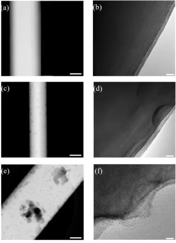
Structural characterization was performed on the passivated NWs with STEM-HAADF (Fig. 2 (a), (c), (e)) and HRTEM (Fig. 1(b),(d),(f)). The NWs grown by HVPE were about 100 µm in length and from 100 to 500 nm in diameter. The NWs passivated at room temperature - sample A in Fig. 2 (a), (b) - exhibited the usual surface observed on as-grown (unpassivated) GaAs NWs with a 2 nm-thick native oxide layer [7]. The annealing step at 620 °C (sample B) generated an observable surface roughness (Fig. 2 (c), (d)). The passivation process at high temperature (sample C) induced large defects (pits) in the NWs surface (Fig. 2 (e), (f)). These observations are consistent with those previously observed on GaAs substrates [24]. Moreover, these observations were regular along the entire length of NWs, meaning the radical nitrogen atoms generated by the ECR plasma source can reach the whole NWs surface; i.e. the nitridation process is homogeneously achieved all along the entire NW.
Figure 2. STEM-HAADF (left) and HRTEM (right) images of HVPE grown GaAs NWs with: (a-b) Sample A: N passivation at room temperature, (c-d) Sample B: N passivation at room temperature and annealed at 620 °C, and (e-f) Sample C: N passivation at 530 °C and annealing at 620 °C. Scale bars are 100 nm for STEM-HAADF images and 5 nm for HRTEM images.
The EELS spectra of Fig. 3 exhibited a clear peak near 401 eV (dashed line) identified as the nitrogen K edge for sample B and C; it was not present in sample A. Thus, a thermal treatment (sample B or C) was required to generate a nitride layer along the NWs surface. These findings are consistent with the passivation results obtained in planar GaAs (100) substrates using the same ECR plasma source [18] [25] .
4
Figure 3. EELS spectra on GaAs NWs after different N passivation conditions.
The EELS-STEM spectrum-imaging mode gives access to spatially-resolved electron energy loss. EELS mapping, reported in Fig. 4, revealed that oxygen is present (Fig. 4(c), (j) and (o)), presumably as a native oxide on the NW surface. This fact is in agreement with HRTEM measurements reported in Fig. 2 (b), (d) and (f), showing a 2-5 nm thick oxide shell even after the passivation processes. However, in sample A where passivation was performed at room temperature, the nitrogen concentration was much lower (Fig. 4(d)) as compared to sample B (Fig. 4(i)) and sample C (Fig. 4(n)) where a thermal treatment was performed, consistent with the results of Fig. 3. Moreover, if the nitridation is performed at high temperature (530 °C, sample C), a thicker nitride layer is formed at the GaAs surface [18] and is revealed by an increase of N concentration from sample B (Fig. 4(i)) to sample C (Fig. 4 (n)). When plasma nitridation is performed at room temperature, the oxygen remains present on the surface. When nitridation is performed at high temperature, the nitrogen concentration becomes higher and the oxidation of the surface due to air exposure is reduced.
Figure 4. From left to right, HAADF-STEM image of NWs, and EELS chemical map of Ga, As, N and O for
(a-e) Sample A: N passivation at room temperature, (f-j)
Sample B: N passivation followed by annealing at 620 °C,
and (k-o) Sample C: Npassivation at high temperature
followed by annealing at 620 °C. Scale bars are 10 nm.
To further understand the effect of N passivation on our GaAs NWs, low temperature (10 K) µ-PL measurements were performed (Figure 5) on reference (as-grown) GaAs NWs without any passivation process, room temperature passivated NWs (sample A), and room temperature N-passivated and 620 °C annealed NWs (sample B). Sample C NWs were not assessed due to the surface damage induced by the high-temperature plasma process, which is deemed unsuitable for applications. The passivation at room temperature (sample A) clearly improved the PL intensity compared to the unpassivated sample, indicating a reduction in non-radiative surface states. In addition, the annealing step (sample B) further improved the PL intensity; this point is consistent with the increased surface nitridation observed in the EELS spectra. The efficacy of the passivation process is therefore active even after 18 months of air exposure. Two main peaks were observed in our PL spectra at 1.46 eV and 1.506 eV. The peak at 1.46 eV is attributed to transitions involving impurities or defects, while the peak at 1.506 eV corresponds to the near band gap emission in GaAs [26][27].
5
These NWs exhibited n-doped behaviour as demonstrated previously through a µ-PL analysis and theoretical study. The non-intentional n-doping is attributed to the incorporation of Si atoms from the substrate [28]. In addition to these two main lines, another emission near 1.49 eV was observed only in N-passivation samples (most evident in sample B). Since we did not observe this peak in the unpassivated sample, the origin of this peak is likely due to the presence of N as observed previously in GaAs [28] [29] [30][31]
Figure 5. µ-PL measurements of unpassivated NWs, NWs after room temperature N-passivation (sample A); after room temperature N-passivation and 620 °C annealing (sample B); after N-passivation at 530 °C and annealed at 620 °C (sample C).
4. Conclusion
We have reported the structural and optical characterization of HVPE-grown ultra-long GaAs NWs. Different experimental conditions were investigated with an ECR source for nitrogen plasma passivation. HRTEM and EELS analysis revealed that the surface nitridation is improved with a thermal annealing treatment, but the roughness of the surface increased for plasma treatment at high temperature. The surface passivation was confirmed by µ-PL spectroscopy which revealed the enhancement of the luminescence with N plasma treatment. Thus, the latter was demonstrated as an effective and simple method for surface passivation in ultra-long NWs, and aims to allow passivation of complex nano-objects.
Acknowledgements
This work has been financially supported by the CPER MMASYF of Region Auvergne-Rhone Alpes that we acknowledge gratefully. It was also funded by: Région Auvergne Rhône-Alpes. Pack ambition recherche; Convention n°17 011236 01 – 61617; the program “Investissements d’avenir” of the French ANR agency, the French government IDEX-SITE initiative 16-µIDEX-0001 (CAP20-25); the European Commission (Auvergne FEDER Funds) and the Region Auvergne in the framework of the LabExIMobS3 (ANR-10-LABX-16-01) and CPER. HH is grateful to the Russian Science Foundation for financial support under the Grant 19-72-30004.
Electron microscopy was performed at the Canadian Centre for Electron Microscopy and supported by the Natural Sciences and Engineering Research Council of Canada.
References
[1]
Yang P, Yan R and Fardy M 2010
Semiconductor nanowire: Whats Next?
6
[2]
Dimakis E, Jahn U, Ramsteiner M,
Tahraoui A, Grandal J, Kong X, Marquardt
O, Trampert A, Riechert H and Geelhaar L
2014 Coaxial multishell (In,Ga)As/GaAs
nanowires for near-infrared emission on Si
substrates Nano Lett. 14 2604–9
[3]
Svensson C P T, Mårtensson T, Trägårdh J,
Larsson C, Rask M, Hessman D, Samuelson
L and Ohlsson J 2008 Monolithic
GaAs/InGaP nanowire light emitting diodes
on silicon Nanotechnology 19 305201
[4]
Thompson M D, Alhodaib A, Craig A P,
Robson A, Aziz A, Krier A, Svensson J,
Wernersson L E, Sanchez A M and
Marshall A R J 2016 Low Leakage-Current
InAsSb Nanowire Photodetectors on Silicon
Nano Lett. 16 182–7
[5]
Harmand J C, Patriarche G, Ṕŕ-Laperne N,
Ḿrat-Combes M N, Travers L and Glas F
2005 Analysis of vapor-liquid-solid
mechanism in Au-assisted GaAs nanowire
growth Appl. Phys. Lett. 87 1–3
[6]
Gutsche C, Lysov A, Regolin I, Blekker K,
Prost W and Tegude F 2011 n -Type
Doping of Vapor – Liquid – Solid Grown
GaAs Nanowires 1–6
[7]
Ramdani M R, Gil E, Leroux C, André Y,
Trassoudaine A, Castelluci D, Bideux L,
Monier G, Robert-Goumet C and Kupka R
2010 Fast growth synthesis of GaAs
nanowires with exceptional length Nano
Lett. 10 1836–41
[8]
Plante M C and LaPierre R R 2008 Control
of GaAs nanowire morphology and crystal
structure Nanotechnology 19 495603
[9]
Dufouleur J, Colombo C, Garma T,
Ketterer B, Uccelli E, Nicotra M and
Fontcuberta I Morral A 2010 P-Doping
mechanisms in catalyst-free gallium
arsenide nanowires Nano Lett. 10 1734–40
[10] Spirkoska D, Arbiol J, Gustafsson A,
Conesa-Boj S, Glas F, Zardo I, Heigoldt M,
Gass M H, Bleloch A L, Estrade S, Kaniber
M, Rossler J, Peiro F, Morante J R,
Abstreiter G, Samuelson L and Fontcuberta
I Morral A 2009 Structural and optical
properties of high quality
zinc-blende/wurtzite GaAs nanowire
heterostructures Phys. Rev. B - Condens.
Matter Mater. Phys. 80 1–9
[11] Dubrovskii V G, Borie S, Dagnet T,
Reynes L, André Y and Gil E 2017
Nucleation and initial radius of
self-catalyzed III-V nanowires J. Cryst. Growth
459 194–7
[12] Lauhon L J, Gudiksen M S and Lieber C M
2004 Semiconductor nanowire
heterostructures Philos. Trans. R. Soc. A
Math. Phys. Eng. Sci. 362 1247–60
[13] Sköld N, Karlsson L S, Larsson M W,
Pistol M E, Seifert W, Trägårdh J and
Samuelson L 2005 Growth and optical
properties of strained GaAs-Gaxin 1-xP
core-shell nanowires Nano Lett. 5 1943–7
[14] Noborisaka J, Motohisa J, Hara S and
Fukui T 2005 Fabrication and
characterization of freestanding
GaAs/AlGaAs core-shell nanowires and
AlGaAs nanotubes by using selective-area
metalorganic vapor phase epitaxy Appl.
Phys. Lett. 87 28–31
[15] Tajik N, Peng Z, Kuyanov P and Lapierre
R R 2011 Sulfur passivation and contact
methods for GaAs nanowire solar cells
Nanotechnology 22 225402
[16] Alekseev P A, Dunaevskiy M S, Ulin V P,
Lvova T V., Filatov D O, Nezhdanov A V.,
Mashin A I and Berkovits V L 2015 Nitride
surface passivation of GaAs nanowires:
Impact on surface state density Nano Lett.
15 63–8
[17] Monier G, Bideux L, Robert-Goumet C,
Gruzza B, Petit M, Lábár J L and Menyhárd
M 2012 Passivation of GaAs(001) surface
by the growth of high quality c-GaN
ultra-thin film using low power glow discharge
nitrogen plasma source Surf. Sci. 606 1093–
9
[18] Mehdi H, Monier G, Hoggan P E, Bideux
L, Robert-Goumet C and Dubrovskii V G
2018 Combined angle-resolved X-ray
photoelectron spectroscopy, density
functional theory and kinetic study of
nitridation of gallium arsenide Appl. Surf.
Sci. 427 662–9
7