HAL Id: hal-02267954
https://hal.archives-ouvertes.fr/hal-02267954
Submitted on 25 Aug 2020
HAL is a multi-disciplinary open access
archive for the deposit and dissemination of
sci-entific research documents, whether they are
pub-lished or not. The documents may come from
teaching and research institutions in France or
abroad, or from public or private research centers.
L’archive ouverte pluridisciplinaire HAL, est
destinée au dépôt et à la diffusion de documents
scientifiques de niveau recherche, publiés ou non,
émanant des établissements d’enseignement et de
recherche français ou étrangers, des laboratoires
publics ou privés.
Evidence for a narrow band gap phase in 1T’ WS 2
nanosheet
Debora Pierucci, Jihene Zribi, Clément Livache, Charlie Gréboval, Mathieu
Silly, Julien Chaste, Gilles Patriarche, Damien Montarnal, Emmanuel
Lhuillier, Abdelkarim Ouerghi, et al.
To cite this version:
Debora Pierucci, Jihene Zribi, Clément Livache, Charlie Gréboval, Mathieu Silly, et al.. Evidence for
a narrow band gap phase in 1T’ WS 2 nanosheet. Applied Physics Letters, American Institute of
Physics, 2019, 115 (3), pp.032102. �10.1063/1.5091997�. �hal-02267954�
1
Evidence for a Narrow Band Gap Phase in 1T’ WS
2Nanosheet
Debora Pierucci
1, Jihene Zribi
2, Clément Livache
3, Charlie Gréboval
3, Mathieu G. Silly
4, Julien
Chaste
2, Gilles Patriarche
2, Damien Montarnal
5, Emmanuel Lhuillier
3*, Abdelkarim Ouerghi
2*,
Benoit Mahler
61 CELLS–ALBA Synchrotron Radiation Facility, Carrer de la Llum 2-26, 08290 Cerdanyola del Valles, Barcelona, Spain
2Centre de Nanosciences et de Nanotechnologies, CNRS, Univ. Paris-Sud, Université Paris-Saclay, C2N – Palaiseau, 91120 Palaiseau, France
3Institut des Nanosciences de Paris, UPMC-CNRS UMR 7588, 4 place Jussieu, boîte courrier 840, 75252 Paris cedex 05, France.
4 Synchrotron-SOLEIL, Saint-Aubin, BP48, F91192 Gif sur Yvette Cedex, France
5Univ Lyon. Université Claude Bernard Lyon 1, CPE Lyon, CNRS, UMR 5265, Chemistry, Catalysis, Polymers and Processes, 43 Bvd du 11 Novembre 1918, F-69616 Villeurbanne, France
6 Institut Lumière-Matière, CNRS UMR 5306, Université Lyon 1, Université de Lyon, 69622 Villeurbanne CEDEX, France.
To whom correspondence should be sent:
el@insp.upmc.fr
abdelkarim.ouerghi@c2n.upsaclay.fr
Abstract :
While 1T’ phase-pure MX2 (M= Mo, W; X= Se, Te) have recently been reported to be superconductors, Weyl semimetals or quantum spin Hall insulators, the electronic properties of phase-pure 1T’-WS2 samples are still lacking thorough investigation. Here we report the study of single-layer 1T’WS2 nanosheets prepared from lithium exfoliation of WS2. We confirmed the composition and structure of single layer 1T’-WS2 flakes using X-ray photoelectron spectroscopy, Raman spectroscopy and aberration corrected transmission electron microscopy (STEM). The distorted octahedral structure related to the 1T’ phase with a 2a×2a superstructure is evidenced using STEM. Photoemission and electronic measurements uncover the presence of a narrow band gap (> 120 meV) in the 1T’-WS2 nanosheets, which is completely different from semiconducting bulk or single-layer 1H-WS2. The material is found to be ambipolar with a p-type nature. At low temperatures, a slow photoresponse is also observed.2
The discovery of novel exotic properties in graphene such as quantum Hall effect at room temperature1,2 has stimulated intensive studies to search for new atomic-layer materials with new functional properties. Among many atomic-layer materials, transition-metal dichalcogenides (TMDs) have attracted significant attention because they provide a versatile platform to combine and vary constituent atoms and crystal structures3–10, that give rise to various exotic properties.Monolayer (ML) TMDs [here, we define “monolayer” as a unit of three atomic layers (chalcogen(X)−metal (M)−chalcogen(X))] are categorized into two different polytypes, 1H and 1T, according to the difference in the coordination of six chalcogen atoms around the metal atom. In the 1H polytype the metal atoms present a trigonal prismatic coordination and the system can be described by hexagonal symmetry (D3h group). In this geometry, the chalcogen atoms are aligned along the vertical axis as “ABA” stacks where A is the chalcogen atom and B is the transition metal atom, respectively. In contrast, the 1T phase presents an octahedral coordination with a tetragonal symmetry (D3d). In this case, an “ABC” stacking is present since one chalcogen layer is shifted with respect to the other.
Typically, in ML TMDs, one of these two possible polytypes represents the thermodynamically stable phase. The thermodynamic selectivity between 1H and 1T phases is strongly related to the number of electron in the d orbitals of the transition metals and enables a straightforward tuning of the properties of TMDs9,11. For the octahedral environment of the 1T phase, the d orbitals are split into the t2g triplet (dxy, dxz, dyz) and the eg doublet (𝑑𝑧2, 𝑑𝑥2−𝑦2)
with the orbitals along the bond directions (t2g) having lower energy. In the trigonal geometry of 1H, the orbital perpendicular to the plane (𝑑𝑧2) lies about 1 eV below those in plane (doublet 𝑑𝑥2−𝑦2, dxy), and the highest energy level is the remaining doublet, dxz, dyz12,13. Group VI TMDs (where M = Mo or W and X = S, Se and Te) with 2 d-electrons per unit cells are usually in the 1H phase, with a fully occupied 𝑑𝑧2 level and large gap to the next occupied
state. This electronic configuration makes 1H-TMDs semiconductors. Additional d-electrons make the 1T structure, with its triplet t2g ground state, more favorable14. Partial filling of the degenerate t2g state (with room for six electrons), makes these materials metallic15. However, it has also been reported that in the case of group VI TMDs the 1T phase is typically unstable and undergoes a spontaneous lattice distortion into a super lattice structure with a 1T’ distorted phase (or distorted octahedral phase). This 1T’ phase has been observed in several experiments concerning group VI TMDs10,16–20. Group VI TMDs in 1T’ phase are predicted to present intriguing quantum phenomena such as quantum spin Hall effect and Weyl states. In fact, the distorted octahedral 1T’ phase is responsible for an intrinsic band inversion near the Fermi level leading to the topological phase transition from trivial to non-trivial band structures12,21. This band inversion, also called p-d type band inversion, involves the chalcogen-p band that is pulled down below the metal-d band around the Γ point of the Brillouin zone and is predicted by DFT calculation to be present in all VI TMDs in the 1T’ phase. In particular, 1ML 1T’ TMDs are predicted to be quantum spin Hall (QSH) insulator with band gaps of the order of tens meV3,21–24, opening the possibility to realize very efficient QSH-based devices. Until now there were only few experimental measurements of this band gap in the case of 1T’ TMDs19,23. In particular, no experimental evidence was shown for WS2. Moreover, this 1T’ phase also present interesting applications beyond electronics, e.g., a low cost catalytic substitute of Pt in electrochemically-assisted production of hydrogen25–27. It is highly desirable to develop well-controllable methods for the preparation of 2D 1T’ TMDs with high purity.
3
Here we present a straightforward approach to synthesize single layer 1T’-WS2 nanosheets with the ratio of this phase exceeding 80%. The presence of the 1T’ phase was revealed using a combination of different techniques: X-ray photoelectron spectroscopy (XPS), micro Raman spectroscopy and aberration corrected scanning transmission electron microscopy (STEM). We report electrical results on 1T’-WS2, finding a photoconductivity effect at low temperature, which is consistent with the presence of a small electronic band gap. This work opens a pathway towards the use of 1T’-WS2 for integrated device structures whose operation relies on the control of topological states and phases.METHODS
a. WS2 nanosheet preparation
Chemicals were purchased from Sigma-Aldrich and used as received without purification. The preparation of 1T’-WS2 monolayers is adapted from refs27,28. All the following reactions are conducted with glassware dried with a flame before use. Proper air-free manipulation techniques are used due to the reactivity and nature of n-butyllithium. Briefly, 300 mg of WS2 powder are added in a Schlenk vessel under Argon. 3 mL of 1M n-butyllithium solution in hexane are added to disperse the WS2 powder, and then the Schlenk vessel is closed with a Teflon stopper and heated at 65 °C for 48 hours. The resulting Li-intercalated WS2 dispersion is then carefully filtered through a Schlenk-frit and rinsed with n-hexane. The WS2 nanosheets disperse readily after addition of water and sonication. The lithium byproducts and large aggregates are discarded by repeated centrifugation. Finally the exfoliated 1T’-WS2 dispersion is diluted to obtain a concentration of 1 mg.mL-1.
b. Photoemission measurements
XPS experiments were carried out on the TEMPO beamline (SOLEIL synchrotron facility) at room temperature29. The photon source was a HU80 Apple II undulator set to deliver linearly polarized light. The photon energy was selected using a high-resolution plane grating monochromator, with a resolving power E/ΔE that can reach 15,000. The end-station is fitted with a modified 200 nm hemispheric electron analyzer (Scienta SES2002, acceptance angle ± 8°) equipped with a delay line detector30. During the XPS measurements, the photoelectrons were detected at 0° from the sample surface normal 𝒏⃗ and at 43° from the polarization vector 𝐸⃗⃗. The W 4f and S 2p spectra were measured at a photon energy hυ = 340 eV (overall resolution ≈100 meV) and the valence band spectrum at hυ = 60 eV (overall resolution ≈60 meV). The spot size was 100 × 80 (H×V) μm2. A Shirley background was subtracted in the core level spectra. The W4f and S 2p spectra were fitted by sums of Voigt curves, i.e, the convolution of a Gaussian by a Lorentzian. The zero binding energy (BE) (i.e. the Fermi level) was taken at the leading edge of a clean gold crystal. This value was determined using a sigmoid fitting in which the standard deviation of the xhalf value (inflection point of the sigmoid) is
0.02 eV.4
c. Transmission electron microscopy
The WS2 flakes are dropcast onto a copper grid with carbon coating. They are then degassed overnight under secondary vacuum to remove any solvent and volatile organic.
d. Transport measurements • Electrodes fabrication
Glass substrates are first cleaned by rinsing with acetone, then sonication in acetone for 5 min, further rinsing with acetone and isopropanol, and finally O2 plasma etching for 5 min. Then AZ5214E resist is spin-coated on the substrate and the substrate is baked at 110 °C for 90 s. UV illumination through a shadow mask is conducted for 2 s, with a black paper below the substrate. The resist is then baked again at 125 °C for 2 min, re-exposed to UV (without mask) for 40 s and developed using AZ726 developer. The film is then rinsed with water and finally dried. A new plasma etching is conducted to remove the remaining organic layer in the exposed areas. The substrates are introduced in a thermal evaporator where 5 nm of chromium and 80 nm of gold are evaporated. The remaining resist is removed by dipping the film in acetone for one hour. The electrodes are then cleaned by a flow of isopropanol and finally dried. The obtained interdigitated electrodes include 25 digits. The spacing between digits is 20 µm. Each digit is 2.5 mm long. The optical area of the device is 0.037 cm2.
• Thin film preparation
A drop of the WS2 nanosheet dispersed in water is dropcasted on a hot plate at 50 °C and dried under ambient conditions on the top of the interdigitated electrodes. Material is added on the surface of the electrodes until we observe a finite resistance.
• Electrolyte gating
For electrolyte gating, we first mixed in a glove box 0.5 g of LiClO4 with 2.3 g of PEG (MW = 6 kg.mol-1). The vial is heated at 170 °C on a hot plate for 2 h until the solution gets clear. To use the electrolyte the solution is warmed around 100 °C and brushed on the top of the WS2 film. A copper metallic gate is then deposited on the top of the electrolyte and used as top gate.
• Electrical measurements
The transport measurements are conducted while the sample is installed on the cold finger of the cryostat under secondary vacuum. The bias is applied using a Keithley 2634B which role is also to measure the collected current. For measurements under illumination, a blue (405 nm) laser diode is shone on the sample.
5
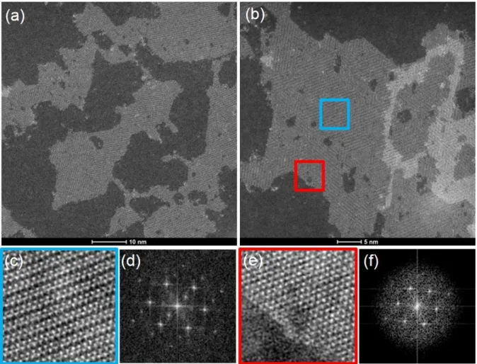
WS2 monolayers were synthesized via a Li exfoliation which gives rise to a high concentration of distorted octahedral 1T-WS2 structure (1T’-WS2)27,31. The synthesized 1T’-WS2 layers were then dispersed in ethanol. After ultra-sonication of the 1T’-WS2 suspension, a few drops of solution were deposited on a substrate (SiO2 for Raman spectroscopy and graphene32–34 for XPS analysis). Aberration-corrected scanning transmission electron microscopy (STEM) is used to determine the structural properties of the synthesized WS2. Figure 1(a) and (b) show two typical STEM images of 1T’-WS2 flakes, on which both mono and bilayers are clearly visible. The structure of these triangular crystals is determined by micro-Raman spectroscopy (discussed later). These images show that atomically thin flakes with a triangular shape and sharp edges have effectively been formed on the SiO2/Si substrate. The sample is composed of high-density monolayer WS2 in the distorted octahedral phase (1T’) (Figure 1, zoom in the blue box) with a 2a × 2a superstructure as confirmed by the FFT pattern. Only on the edges of the sheet, few areas characterized by the trigonal phase (1H) (Figure 1, zoom in the red box) have been found.Figure 1: a) Typical STEM image of single layer 1T’-WS2 nanosheets, b) Typical STEM image of mono and bilayer 1T’-WS2 nanosheets, c) Atomic resolution STEM image. The asymmetric distribution of atoms is clearly shown, d) Corresponding FFT diffraction of 1T’-WS2 nanosheets (zoom in the blue box), e) and f) Atomic resolution STEM image and corresponding FFT of 1H-WS2 nanosheets (zoom in the red box).
6
The presence of the 1T’- phase can also be established by micro-Raman analysis27. The Raman spectrum of the WS2 sample deposited on SiO2 is shown in Figure 2a (blue line). The spectra are obtained under 532 nm excitation with a spot diameter of about 1 μm and incident power about 40 μW at room temperature. The spectrum displays the modes J1,J2 and J3 that are attributed to the 1T’-phase of WS227,35–37. When increasing the laser power up to 800 μW, a laser-induced heating process occurs. The local increase of temperature is responsible for a phase transition from 1T’to 1H27 as shown in Figure 2(a) (red curve). In fact, the J1, J2 and J3 peaks of the 1T’-WS2 almost disappear while the in-plane 𝐸2𝑔1 and out-of-plane 𝐴1𝑔 modes of 1H-WS2 are now clearly visible on the spectrum.38,39 XPS spectroscopy, see Figure2(b) and (c) was also used to further investigate the 1T’-WS2 nanosheets. After sonication of the 1T’-WS2 suspension, a few drops of solution were deposited on epitaxial graphene for XPS measurements. Monitoring the binding energy of the W 4f and S 2p core level peaks allows to unambiguously distinguish between the 1H and 1T’ structures of WS2. The W 4f core levels can be deconvoluted, as shown in Figure 2 (b) into four components, three composed by the W 4f5/2 as well as the W 4f7/2 doublet shifted by 2.18 eV (ratio of 0.75) and the W 5p3/2 (located at a binding energy BE = 37.9 eV). The main doublet (light blue curves), where the W 4f 7/2 peak is located at a BE = 31.9 eV, represents the signature of the 1T’ phase of WS239–43. The other two smaller doublets with the W 4f 7/2 located at BE = 32.7 eV (purple curves) and 35.7 eV (green curves) are related to the 1H phase and the oxidized state (i.e. WO3), respectively40–
45.The XPS deconvolutions of W 4f and S 2p (see SI figure S1) peaks confirm that 80 % of the sample consists of
WS2 in the 1T’ phase. The photoemission spectra of the valence band, measured with photon energy of 60 eV, are shown in Figure 2(c) (blue dots). On the same graph, the Fermi edge of a clean gold sample measured exactly in the same experimental conditions is also shown (black triangles). The zero of the binding energy (i.e., the Fermi level) was taken at the leading edge of this gold sample. From the intersection of the linear extrapolation of the leading edge of the valence band spectrum with the baseline, we can determine the position of the valence band maximum (VBM)46. As we can see, the valence band maximum of the 1T’ WS2 sample is not exactly at the Fermi level but at a BE= 60 meV (see SI, section 1). This is the signature of a presence of a narrow bandgap, unlike for the metallic 1T phase. Due to the p –type nature of the sample, before gating, as discussed later in the text, this suggest that the band gap is larger than 120 meV3,21–24. Infrared absorption (Figure S3b), indeed exhibit a strong increase of the absorption around 200 meV range, which may result from this band gap.
7
Figure 2 (a) Micro-Raman spectra in the wavenumber region between 200 and 450 cm-1 of 1T’WS2 at two different powers; 40 μW (blue data) and 800 μW (red data). High resolution XPS of 1T’-WS2: (b) W 4f spectrum at hυ=340 eV, (c) Integrated valence band photoemission spectrum acquired at hυ = 60 eV of 1T’-WS2 is compared to the Fermi level reference collected on a gold crystal at the same photon energy. The electron analyser acceptance angle was ± 8° and the photoelectrons were detected at 0° from the sample surface normal 𝒏⃗.The evidence for a narrow bandgap phase can be further investigated using transport measurements. A thin film of WS2 nanosheets is dropcasted on pre-prepared interdigitated electrodes and dried at room temperature to avoid any phase change. No further heat or chemical treatment is applied to the film before its use. At room temperature the material is conductive, see Figure 3 (a). Once the sample is introduced into a cryostat and cooled down, its electrical conductivity drops, see Figure 3 (a) and (c-e). An Arrhenius fit, of the temperature dependence of the current, near room temperature (300-200K), reveals a low activation energy of 32 meV, see Figure S4. This weak value is incompatible with the existence of a wide band gap phase where activation energy close to half the optical band gap would have been expected. For sake of comparison we have obtained an activation energy of 172 meV for the 1H phase of WS2 obtained from exfoliation with N-methyl-pyrrolidone, see Figure S6a The transport in film of WS2 nanosheets is expected to occur through a hopping process. At low temperatures, variable range hopping47 is expected to occur. The scaling of the conductance with temperature is of utmost interest to discriminate transport between metallic and semiconductor grains. In the case of metallic grains, the high density of state of the material implies that hopping is only limited by the electrostatic cost to inject carriers. In this case, Efros-Shklovskii scaling (𝜎𝛼 𝑒𝑥𝑝(−(𝑇𝐸𝑆/𝑇)1/2)) of the conductance with temperature is expected48. On the other hand, for semiconductor
grains, the sparse density of state of the material is limiting the hopping and a Mott scaling is expected for the temperature dependency of the conductance: 𝜎𝛼 𝑒𝑥𝑝(−(𝑇𝑀/𝑇)1/4). Such fit of the conductance is plotted in Figure
8
The lack of metallic nature is further confirmed by a field effect transistor measurement. Recently Papadopoulos etal49 have conducted transport measurements on the 1T’ phase of MoS2 and no gate effect has been observed using conventional back gating through a dielectric. Here we rather choose to use ion gel gating of the film by a mixture of LiClO4 dissolved in polyethylene glycol50,51. Beyond the large capacitance of the electrolyte compared to conventional dielectric, this method allows air operability and to gate thick films thanks to the percolation of the ions within the array of nanosheets. The transfer curve (drain current as a function of gate bias) reveals a clear ambipolar behavior with both hole and electron conductions, see Figure 3(b). The minimum of conductance appears at positive gate bias, which suggests the presence of an inherent p-type character in absence of gate. The on/off ratio is small typically a factor 2. If a purely metallic phase was present, no current modulation would have been observed. On the other hand, for the 1H wide band gap semiconductor phase, a much stronger modulation is obtained see Figure S6 and ref52. As a result, we can conclude that transport measurements exclude the possibility of both fully metallic and wide bandgap phases and support the existence of a narrow band gap material53. This result also differs from the one obtained on the 1T’ phase of MoS2, for which the lack of gating effect17,49 or the I-T dependence37 rather suggests a stronger metallic character compared to the 1T’ phase of WS2.
To finish, we investigated the photoconductive properties of the WS2 nanosheet film. At room temperature and under illumination, no photoconductive properties are observed. On the other hand, at low temperature, typically for T < 100 K a clear conductance modulation is observed, see Figure 3(d) and (e). Again, this behavior is consistent with a narrow bandgap material behavior since metallic materials would have presented no modulation even at low temperature. For sake of comparison, we have also checked that the 1H phase (ie the wide band gap semiconductor phase) of the material present a much stronger modulation, see Figure S7. The photoresponse of the 1T’ is extremely slow and we measured the 3 dB cut-off frequency to be 0.16 Hz, see Figure S5. The origin of this persistent photoresponse remains unclear for the moment.
In conclusion, we have used a facile and reproducible method for achieving monolayer 1T’-WS2 flakes. Samples were carefully studied using XPS, Raman spectroscopy, and STEM to confirm their atomic compositions and structural configurations. We observed that while the ML 1T-WS2 holds metallic character, the 1T’ counterpart exhibits a semiconducting nature. This semiconducting nature is then confirmed using photoemission and (photo)-transport measurements. The material is found to be ambipolar with a p-type nature in absence of gate. At low temperature, a slow photoresponse is also observed. The present study opens a pathway toward developing next-generation electronic and spintronic nanodevices based on ML TMDs.
9
Figure 3 (a) I-V curve for a thin film of WS2 nanosheets at different temperatures. (b) Transfer curve (drain and gate current) as a function of the applied gate bias for a thin film of WS2 nanosheets gated by ion gel electrolyte. (c) Current as function of temperature for a thin film of WS2 nanosheets as a function of T-1/4 .The drain source bias is set to 10 mV (d) I-V curve for a thin film of WS2 nanosheets measured at 25 K under dark condition and under illumination by a blue (λ=405 nm) laser diode (P=10 mW). (e) Current under dark condition and under illumination (λ=405 nm - P=10 mW) as a function of temperature.Supplementary material
See supplemental material at [URL will be inserted by AIP] for additional data about material preparation,
as well as the XPS and transport measurements.
10
We acknowledge support from the Agence Nationale de la Recherche (ANR) under grants Labex Nanosaclay and H2DH (ANR-15-CE24-0016). Labex Nanoscalay belongs to the public funded Investissements d’Avenir program managed by ANR. EL thanks the support ERC starting grant blackQD (grant n° 756225). We acknowledge the use of clean-room facilities from the “Centrale de Proximité Paris-Centre”. This work has been supported by the Region Ile-de-France in the framework of DIM Nano-K (grant dopQD). This work was supported by French state funds managed by the ANR within the Investissements d'Avenir programme under reference ANR-11-IDEX-0004-02, and more specifically within the framework of the Cluster of Excellence MATISSE and also by the grant IPER-Nano2.Competing financial interests: The authors declare no competing financial interests.
REFERENCES
1
K.S. Novoselov, Z. Jiang, Y. Zhang, S. V Morozov, H.L. Stormer, U. Zeitler, J.C. Maan, G.S. Boebinger, P.
Kim, and A.K. Geim, Science (New York, N.Y.) 315, 1379 (2007).
2
C.L. Kane and E.J. Mele, Physical Review Letters 95, 226801 (2005).
3
Y. Ma, L. Kou, X. Li, Y. Dai, S.C. Smith, and T. Heine, Physical Review B 92, 085427 (2015).
4
A. Pulkin and O. V. Yazyev, Journal of Electron Spectroscopy and Related Phenomena 219, 72 (2017).
5D. Xiao, G. Bin Liu, W. Feng, X. Xu, and W. Yao, Physical Review Letters 108, 1 (2012).
6
N.F.Q. Yuan, K.F. Mak, and K.T. Law, Physical Review Letters 113, 097001 (2014).
7Z.Y. Zhu, Y.C. Cheng, and U. Schwingenschlögl, Physical Review B 84, 153402 (2011).
8
A. Roth, C. Brüne, H. Buhmann, L.W. Molenkamp, J. Maciejko, X.-L. Qi, and S.-C. Zhang, Science (New
York, N.Y.) 325, 294 (2009).
9
D. Voiry, A. Mohite, and M. Chhowalla, Chemical Society Reviews 44, 2702 (2015).
10
C. Guo, J. Pan, H. Li, T. Lin, P. Liu, C. Song, D. Wang, G. Mu, X. Lai, H. Zhang, W. Zhou, M. Chen, and F.
Huang, J. Mater. Chem. C 5, 10855 (2017).
11
B. Ouyang, G. Lan, Y. Guo, Z. Mi, and J. Song, Applied Physics Letters 107, 191903 (2015).
12H. Yang, S.W. Kim, M. Chhowalla, and Y.H. Lee, Nature Physics 13, 931 (2017).
13
W. Zhao, J. Pan, Y. Fang, X. Che, D. Wang, K. Bu, and F. Huang, Chemistry - A European Journal 24, 15942
(2018).
14
M. Kan, J.Y. Wang, X.W. Li, S.H. Zhang, Y.W. Li, Y. Kawazoe, Q. Sun, and P. Jena, Journal of Physical
Chemistry C 118, 1515 (2014).
15
M. Chhowalla, H.S. Shin, G. Eda, L.-J. Li, K.P. Loh, and H. Zhang, Nature Chemistry 5, 263 (2013).
16J.C. Park, S.J. Yun, H. Kim, J.-H. Park, S.H. Chae, S.-J. An, J.-G. Kim, S.M. Kim, K.K. Kim, and Y.H. Lee, ACS
Nano 9, 6548 (2015).
17
J.S. Kim, J. Kim, J. Zhao, S. Kim, J.H. Lee, Y. Jin, H. Choi, B.H. Moon, J.J. Bae, Y.H. Lee, and S.C. Lim, ACS
Nano 10, 7500 (2016).
18
Y. Yu, G.-H. Nam, Q. He, X.-J. Wu, K. Zhang, Z. Yang, J. Chen, Q. Ma, M. Zhao, Z. Liu, F.-R. Ran, X. Wang,
H. Li, X. Huang, B. Li, Q. Xiong, Q. Zhang, Z. Liu, L. Gu, Y. Du, W. Huang, and H. Zhang, Nature Chemistry
10, 638 (2018).
19
S. Tang, C. Zhang, D. Wong, Z. Pedramrazi, H.-Z. Tsai, C. Jia, B. Moritz, M. Claassen, H. Ryu, S. Kahn, J.
Jiang, H. Yan, M. Hashimoto, D. Lu, R.G. Moore, C.-C. Hwang, C. Hwang, Z. Hussain, Y. Chen, M.M. Ugeda,
Z. Liu, X. Xie, T.P. Devereaux, M.F. Crommie, S.-K. Mo, and Z.-X. Shen, Nature Physics 13, 683 (2017).
11
20
L. Liu, J. Wu, L. Wu, M. Ye, X. Liu, Q. Wang, S. Hou, P. Lu, L. Sun, J. Zheng, L. Xing, L. Gu, X. Jiang, L. Xie,
and L. Jiao, Nature Materials 17, 1108 (2018).
21
D.-H. Choe, H.-J. Sung, and K.J. Chang, Physical Review B 93, 125109 (2016).
22X. Qian, J. Liu, L. Fu, and J. Li, Science (New York, N.Y.) 346, 1344 (2014).
23
P. Chen, W.W. Pai, Y.-H. Chan, W.-L. Sun, C.-Z. Xu, D.-S. Lin, M.Y. Chou, A.-V. Fedorov, and T.-C. Chiang,
Nature Communications 9, 2003 (2018).
24
M.M. Ugeda, A. Pulkin, S. Tang, H. Ryu, Q. Wu, Y. Zhang, D. Wong, Z. Pedramrazi, A. Martín-Recio, Y.
Chen, F. Wang, Z.-X. Shen, S.-K. Mo, O. V. Yazyev, and M.F. Crommie, Nature Communications 9, 3401
(2018).
25
G. Gao, Y. Jiao, F. Ma, Y. Jiao, E. Waclawik, and A. Du, The Journal of Physical Chemistry C 119, 13124
(2015).
26
A. Ambrosi, Z. Sofer, and M. Pumera, Chemical Communications 51, 8450 (2015).
27
D. Voiry, H. Yamaguchi, J. Li, R. Silva, D.C.B. Alves, T. Fujita, M. Chen, T. Asefa, V.B. Shenoy, G. Eda, and
M. Chhowalla, Nature Materials 12, 850 (2013).
28
D. Voiry, A. Goswami, R. Kappera, C. de C.C. e Silva, D. Kaplan, T. Fujita, M. Chen, T. Asefa, and M.
Chhowalla, Nature Chemistry 7, 45 (2015).
29
D. Pierucci, H. Henck, J. Avila, A. Balan, C.H. Naylor, G. Patriarche, Y.J. Dappe, M.G. Silly, F. Sirotti, A.T.C.
Johnson, M.C. Asensio, and A. Ouerghi, Nano Letters 16, 4054 (2016).
30
N. Bergeard, M.G. Silly, D. Krizmancic, C. Chauvet, M. Guzzo, J.P. Ricaud, M. Izquierdo, L. Stebel, P.
Pittana, R. Sergo, G. Cautero, G. Dufour, F. Rochet, and F. Sirotti, Journal of Synchrotron Radiation 18, 245
(2011).
31
B. Mahler, V. Hoepfner, K. Liao, and G.A. Ozin, Journal of the American Chemical Society 136, 14121
(2014).
32
Z. Ben Aziza, D. Pierucci, H. Henck, M.G. Silly, C. David, M. Yoon, F. Sirotti, K. Xiao, M. Eddrief, J.-C. Girard,
and A. Ouerghi, Physical Review B 96, (2017).
33
H. Sediri, D. Pierucci, M. Hajlaoui, H. Henck, G. Patriarche, Y.J. Dappe, S. Yuan, B. Toury, R. Belkhou, M.G.
Silly, F. Sirotti, M. Boutchich, and A. Ouerghi, Scientific Reports 5, 16465 (2015).
34
E. Pallecchi, F. Lafont, V. Cavaliere, F. Schopfer, D. Mailly, W. Poirier, and A. Ouerghi, Scientific Reports
4, 4558 (2014).
35
Y. Sun, R. Wang, and K. Liu, Applied Physics Reviews 4, 011301 (2017).
36
M.S. Sokolikova, P.C. Sherrell, P. Palczynski, V.L. Bemmer, and C. Mattevi, Nature Communications 10,
712 (2019).
37
Q. Liu, X. Li, Z. Xiao, Y. Zhou, H. Chen, A. Khalil, T. Xiang, J. Xu, W. Chu, X. Wu, J. Yang, C. Wang, Y. Xiong,
C. Jin, P.M. Ajayan, and L. Song, Advanced Materials 27, 4837 (2015).
38
A. Berkdemir, H.R. Gutiérrez, A.R. Botello-Méndez, N. Perea-López, A.L. Elías, C.-I. Chia, B. Wang, V.H.
Crespi, F. López-Urías, J.-C. Charlier, H. Terrones, and M. Terrones, Scientific Reports 3, 1755 (2013).
39
H. Henck, Z. Ben Aziza, D. Pierucci, F. Laourine, F. Reale, P. Palczynski, J. Chaste, M.G. Silly, F. Bertran, P.
Le Fèvre, E. Lhuillier, T. Wakamura, C. Mattevi, J.E. Rault, M. Calandra, and A. Ouerghi, Physical Review B
97, 155421 (2018).
40
T.A.J. Loh and D.H.C. Chua, The Journal of Physical Chemistry C 119, 27496 (2015).
41
S.X. Leong, C.C. Mayorga-Martinez, X. Chia, J. Luxa, Z. Sofer, and M. Pumera, ACS Applied Materials &
Interfaces 9, 26350 (2017).
42
T.A.J. Loh, D.H.C. Chua, and A.T.S. Wee, Scientific Reports 5, 18116 (2016).
43A. Ambrosi, Z. Sofer, and M. Pumera, Chemical Communications 51, 8450 (2015).
44
S.K. Kim, W. Song, S. Ji, Y.R. Lim, Y.B. Lee, S. Myung, J. Lim, K.-S. An, and S.S. Lee, Applied Surface Science
425, 241 (2017).
45
F. Perrozzi, S.M. Emamjomeh, V. Paolucci, G. Taglieri, L. Ottaviano, and C. Cantalini, Sensors and
12
46
S.A. Chambers, T. Droubay, T.C. Kaspar, and M. Gutowski, Journal of Vacuum Science & Technology B:
Microelectronics and Nanometer Structures 22, 2205 (2004).
47
A.L. Efros, N. Van Lien, and B.I. Shklovskii, Solid State Communications 32, 851 (1979).
48
H. Moreira, Q. Yu, B. Nadal, B. Bresson, M. Rosticher, N. Lequeux, A. Zimmers, and H. Aubin, Physical
Review Letters 107, 176803 (2011).
49
N. Papadopoulos, G.A. Steele, and H.S.J. van der Zant, Physical Review B 96, 235436 (2017).
50E. Lhuillier, A. Robin, S. Ithurria, H. Aubin, and B. Dubertret, Nano Letters 14, 2715 (2014).
51
H. Henck, D. Pierucci, J. Chaste, C.H. Naylor, J. Avila, A. Balan, M.G. Silly, M.C. Asensio, F. Sirotti, A.T.C.
Johnson, E. Lhuillier, and A. Ouerghi, Applied Physics Letters 109, (2016).
52