HAL Id: hal-01438557
https://hal.archives-ouvertes.fr/hal-01438557
Submitted on 2 Jul 2020HAL is a multi-disciplinary open access archive for the deposit and dissemination of sci-entific research documents, whether they are pub-lished or not. The documents may come from teaching and research institutions in France or abroad, or from public or private research centers.
L’archive ouverte pluridisciplinaire HAL, est destinée au dépôt et à la diffusion de documents scientifiques de niveau recherche, publiés ou non, émanant des établissements d’enseignement et de recherche français ou étrangers, des laboratoires publics ou privés.
2D Colloidal Metal Chalcogenides Semiconductors:
Synthesis, Spectroscopy, and Applications
Emmanuel Lhuillier, Silvia Pedetti, Sandrine Ithurria, Brice Nadal, Hadrien
Heuclin, Benoit Dubertret
To cite this version:
Emmanuel Lhuillier, Silvia Pedetti, Sandrine Ithurria, Brice Nadal, Hadrien Heuclin, et al.. 2D Colloidal Metal Chalcogenides Semiconductors: Synthesis, Spectroscopy, and Applications. Accounts of Chemical Research, American Chemical Society, 2015, 48 (1), pp.22 - 30. �10.1021/ar500326c�. �hal-01438557�
2D Colloidal Metal Chalcogenides Semiconductors: Synthesis, Spectroscopy and Applications Emmanuel Lhuillier1, Silvia Pedetti1,2, Sandrine Ithurria2, Brice Nadal1, Hadrien Heuclin1, Benoit Dubertret2*
1 Nexdot, 10 rue Vauquelin 75005 Paris, France
2 Laboratoire de Physique et d’Etude des Matériaux, ESPCI-ParisTech, PSL Research University, Sorbonne Université
UPMC Univ Paris 06, CNRS, 10 rue Vauquelin 75005 Paris, France *To whom correspondence should be sent: [email protected]
CONSPECTUS :
Semiconductors are at the basis of electronics. Up to now, most devices that contain semiconductors use materials obtained from a top down approach with semiconductors grown by molecular beam epitaxy or chemical vapor deposition. Colloidal semiconductors nanoparticles have been synthesized for more than 30 years now, and their synthesis is becoming mature enough so that these nanoparticles start to be incorporated into devices. An important development that recently took place in the field of colloidal quantum dots is the synthesis of 2 dimensional semiconductor nanoplatelets that appear as free standing nanosheets. These 2D colloidal systems are the newborn in the family of shaped-controlled nanoparticles that started with spheres, was extended with rods and wires, continued with tetrapods, and that now ends with platelets. From a physical point of view, these objects bring the 1D-confined particles into the colloidal family. It is a notable addition, since these platelets can have a thickness that is controlled with atomic precision, so that no inhomogeneous broadening is observed. Because they have two large free interfaces, the mirror charges play an important role, and the binding energy of the exciton is extremely large. These two effects almost perfectly compensate each other, but it results in particles with unique spectroscopic properties such as fast fluorescent lifetimes and extreme color purity (narrow full width at half maximum of their emission spectra). These nanoplatelets with extremely large confinement, but very simple and well defined chemistry, are model systems to check and further develop, notably with the incorporation in the models of the organic/inorganic interface, various theoretical approaches used for colloidal particles. From a chemical point of view, these colloidal particles are a model system to study the role of ligands since they have precisely defined surfaces. In addition, the synthesis of these highly anisotropic objects triggered new research to understand at a mechanistic level how this strong anisotropy could be generated. Luckily, some of the chemical know-how built with the spherical and rod-shaped particles is being transferred – with some adaptation - to the 2D systems, so that 2D core/shell and core/crown hetero-structures have recently been introduced. These objects are very interesting because they suggest that multiple quantum wells, that are at the basis of large-scale applications, could be grown in solution. From the application point of view, 2D colloidal nanoplatelets offer interesting perspectives when color purity, charge conductivity, or field tunable absorption are required. In this account, we review the chemical synthesis, the physical properties and the applications of colloidal semiconductor nanoplatelets with an emphasis on the zinc-blende nanoplatelets that were developed more specifically in our group.
1. Introduction
The discovery of the size dependent optical properties of semiconductor colloidal quantum dots (CQDs) is about 30 years old, and the community of scientists working in the field has recently celebrated this event at ESPCI, in Paris (http://www.30-years-qds.com).1 Although the field started in the early 80s, with the pioneering work of Ekimov,2
Efros3 and Brus,4 it is the first synthesis of spherical colloidal nanocrystals (NCs) with a precise control of the size
dispersion (~5%) in 19935 in the group of Bawendi that established the solution growth of NCs as a very promising
route for the synthesis and the applications of colloidal QDs. Since then, the synthesis of CQDs has been extended to a large variety of materials,6 of compositions7 and of morphology.8 The control of the shape: sphere, rod9, wires10 or
carriers, and as a consequence their density of states. Amongst the different shapes, nanoplatelets (NPLs) are of particular interest because it has been shown that their thickness can be controlled with an atomic precision. Their large planar facets can be precisely defined chemically as it is the case for other 2D systems such as graphene or 2D dichalcogenide12 materials that are also detailed in this special issue. As a consequence, nanoplatelets can serve as a
model system to better understand the effect of surface chemistry, of composition and of confinement in semiconductor systems.
Several reviews on the synthesis of 2D colloidal systems have already been written,13,14 and an other one from the
group of W. Buhro is in this special issue. The reader is referred to these reviews for additional information. In this account, we detail the growth mechanisms of colloidal NPLs, we present the possibility to obtain 2D hetero-structures such as core/shell and core/crown NPLs, either by colloidal synthesis or using cation exchange. We review the unique optical properties of these 2D structures, as well as their use in devices such as light emitting diodes, field effect transistors and photo-detectors.
2. Material
2.1. Growth mechanisms of 2D nanoplatelets
2D metal chalcogenide semiconductor nanoplatelets can be synthesized in three different crystal structures: zinc blende, wurtzite and rock salt. We describe rapidly the synthesis of these three families of NPLs, with an emphasis on the zinc blende NPLs that were developed mainly in our group.
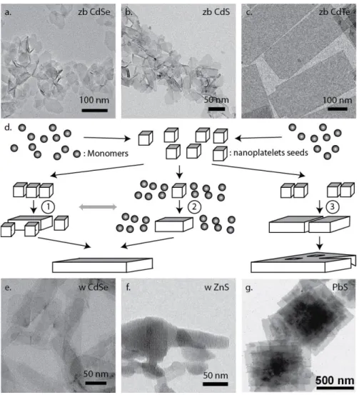
2.1.1. Wurtzite NPLs
In 2006 Hyeon and co-workers reported the synthesis of CdSe nanoribbons15 (Figure 1e) that were obtained thanks to
a lamellar-like template growth induced by the dissolution of cadmium chloride in an amine in which a selenium precursor is slowly reduced. Soon after, CdS16 and CdTe17 nanoribbons were synthesized using similar syntheses. The
growth mechanism of these wurtzite 2D crystals has been investigated by the teams of Hyeon18,19 and Buhro20-22 and
was shown to proceed through the templated assembly of magic size clusters such as CdSe13 or CdSe34 as proposed in
path 1 of figure 1d. ZnS nanoplatelets (Figure 1f) can also be grown by this method, even if the presence of clusters as building blocks has not yet been proven. Wurtzite NPLs are generally synthesized at relatively low temperature (< 100°C), using cadmium acetate or halide precursors in long chain amine solvent. These NPLs have large surfaces that are formed of a mixture of anions and cations.
Figure 1: TEM images of zinc blende CdSe (a) CdS (b), CdTe (c) wurtzite CdSe (e) and ZnS (f), and rock salts PbS (g) NPLs, from ref 23. Reprinted with permission from AAAS. d). Scheme of the different paths for the growth of nanoplatelets. Adapted with permission from reference 24. Copyright (2011) American Chemical Society
2.1.2. Zinc blende NPLs
In 2008, our group reported the first synthesis of zinc blende CdSe nanoplatelets (Figure 1a) with different thicknesses that were controlled with atomic precision.11 In 2011, the syntheses of zinc blende NPLs were extended to CdS and
CdTe25 (Figure 1b and c). In these syntheses, the anisotropy is obtained by mixing a short chain carboxylic acid, with a
cadmium carboxylate with a longer aliphatic chain, so that the cadmium precursors can be assimilated to Cd(R1COO)(R2COO) with R1 either CH3 or C2H5 and R2 an aliphatic chain with more than 10 carbons. The anionic
precursor can either be complexed to TOP, or mixed as a powder in a solvent, usually octadecene. The growth of these nanoplatelets is performed at higher temperature (120-250°C) compared to wurtzite nanoplatelets. The formation of zinc-blende nanoplatelets starts with well-defined seeds with spectral characteristics comparable to so-called “magic sized clusters”.24 These seeds have two cation-rich facets that are poisoned by ligands, and that can extend laterally
through continuous reaction of precursors, as presented in path 2, Figure 1d. This lateral extension can be continuously followed by monitoring the red shift of the excitonic peaks up to the point where the lateral dimensions of these “quantum wells” are larger than 2 times the 2D Bohr radius.26 Below these dimensions, the exciton experiences a 3D
confinement that increases the excitonic energy transition. For larger dimensions, the exciton is purely 1D confined, and the full width at half maximum (FWHM) of the NPL photoluminescence is narrowest (close to kBT). The lateral
extension of NPLs can be performed with continuous injection of precursors to reach lateral dimensions of few hundred nanometers for CdSe27 and CdTe28 NPLs. Today, one can control not only the lateral size and the composition
of the NPLs but also their thickness by varying the reaction conditions.25 For a given synthesis, the latter the acetate
salt is introduced the thicker the NPLs. Similarly, for CdS NPLs, low temperature and shorter aliphatic chains favor thinner NPLs.29
2.1.3. Rock salt NPLs
Apart from zinc-blende and wurtzite NPLs, Weller and co-workers have synthesized in 201023 lead sulfide nanoplatelets
with a rock salt crystal structure, thanks to the oriented attachment of lead sulfide nanocrystals. The introduction of a chloride compound that binds to Pb altered the nucleation and growth of PbS and led to small nanocrystals (< 3 nm) which exhibit the highly reactive (110) facets necessary for the oriented attachment (see path 3 in Figure 1d and g).
2.2. Nanoplatelets heterostructures
2.2.1. Core/shell
As for spherical QDs, the possibility to enrich the landscape of 2-dimensional nanocrystals with heterostructures such as core/shell (Figure 2a) is fascinating. Indeed, deposition of a shell can enhance the optical properties e.g. higher quantum yield and better photostability7,30,31 than core-only NCs. While several methods exist to grow shells on QDs
and rods,32,33 only two techniques have been developed so far to obtain 2D core/shell NPLs such as CdSe/CdS NPLs
(Figure 2a).34,35 The first method, named colloidal atomic layer deposition (c-ALD), allows a fine control of the shell
thickness and its composition. This method consists of an alternate deposition of anionic and cationic monolayers. As mentioned earlier, zinc-blende NPLs have two Cd rich facets passivated with oleate chains. These Cd rich facets can be covered with a sulfide layer using TMS2S, (NH4)2S, Na2S or NaSH.36 This sulfide coverage comes with a ligand exchange
and a transfer of the NPLs from a non-polar to a polar phase.37 The next cationic layer is grown with the reaction of
NPLs with a cadmium salt. At each step of the reaction, the excess of precursors can be removed using precipitation. The second method to make core/shell NPLs is a “one pot” method based on the in situ generation of hydrogen sulfide by the reaction of thioacetamide with octylamine.38 A cadmium source is added and the reaction is let run for a few
hours. Both methods can be successfully applied on different thicknesses and lateral sizes. The absorption spectrum of core/shell NPLs show two excitonic peaks (Figure 2b), red shifted compared to the cores, due to the electron delocalization over the entire thickness of the NPL. Such core/shell NPLs exhibit high QY, up to 80%.39
Figure 2 : (a) scheme of core/shell CdSe/CdS NPLs with its absorption and PL spectra (b) and its TEM picture (c).(d,e,f) Same set of data for core only NPL. (g,h,i) Same set of data for CdSe/CdS core/crown NPLs.
2.2.2. Core crown
Another type of 2D heterostructures has been recently developed. Instead of growing the NPLs along the thickness, extension of the lateral facets is performed. The group of Artemyev and our group have reported the synthesis of CdSe/CdS core/crown NPLs (Figure 2 g,h,i).40,41 As for core NPLs, the lateral extension is achieved by using a
combination of long chain and short chain carboxylate ligands (typically an acetate and an oleate), as it has been used for the lateral extension of CdSe NPLs into CdSe nanosheets.27 The resulting crown has the same thickness as the
starting NPL. Contrary to core/shell structures, almost no red-shift of the emission peak is observed during the growth of the CdS crown. This absence of red shift is explained by the strong (≈300 meV) binding energy of the exciton42 that
is greatly enhanced compared to spherical objects. Because of this large binding energy, the Bohr radius of the exicton is very small (≈1-2 nm), and there is no lateral confinement in the NPLs. Consequently, lateral extension do not produce any PL emission red shift. In these heterostructures, both core and crown sizes can be controlled. These new objects exhibit enhanced photoluminescence compared to the starting core NPLs (up to 60% QY) as well as a very high absorption cross section in the CdS region (Figure 2h). Spectroscopic studies showed that these objects can act as exciton funnels where the excitons are collected in the CdS crown and rapidly and efficiently transferred to the CdSe core where the recombination occurs. Recently the growth of CdTe shell with a type II band alignment was also proposed43.
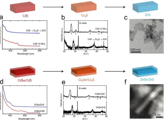
2.3. Expanding the range of available material through cations’ exchange
Recently, cations’ exchange reactions have been developed as an alternative approach to obtain nanoparticles difficult to synthesize by direct methods. Many groups have demonstrated the potential of this method on spherical or rod-shaped core44-46 or core/shell47 nanoparticles. Regarding 2D nano-structures, Moreels et al. have published the
preparation of CdTe nanodisks from Cu2Te by cation exchange.48 The group of Lee has prepared ZnS:Ag2S
heterostructures from ZnS nanosheets.49 Bouet et al. have studied cation exchange on cadmium based 2D shaped
nanoparticles.50 Starting from CdS or CdSe/CdS NPLs, ZnS (Figure 3a-c) and PbS core or ZnSe/ZnS (Figure 3 d-f) and
PbSe/PbS core/shell structures were obtained. During the steps of cations’ exchange, the NPLs’ shape is conserved as long as the thickness of the NPL is larger than 1.8 nm (Figures 3c and 3f). Moreover, after exchange, zinc-based nanostructures exhibit a zinc-blende structure, identical to initial nanoparticles, whereas, with lead, the final structure turns to rock-salt. Finally when exchanging, cations diffuse uniformly from the largest surfaces through the NPLs. Recently, the group of Manna showed that copper selenide- sulfide nanoplatelets could be transformed without morphological change into copper tin zinc selenide-sulfide NPLs.51
Figure 3: Cation exchange on CdS. (a) Absorption spectra, (b) X-rays powder diffraction patterns of CdS NPLs and Zn exchanged NPLs and (C) TEM image of Zn exchanged NPLs. Cation exchange on CdSe/CdS. (a) absorption spectra, (b) X-rays powder diffraction patterns of CdSe/CdS NPLs and Zn exchanged NPLs and (C) TEM image of Zn exchanged NPLs. Adapted with permission from reference 50. Copyright (2013) American Chemical Society
2.4. Other
2.4.1. Self-assembly
Self-assembly of nanoparticles into large and ordered structures, is motivated by the idea to build at the nanoscale engineered hybrids.52,53 However, the real benefice is correlated to the fine control of the three dimensional
organizations of the nanoparticles. Few examples concerning the self-assembly of 2D anisotropic nano-objects exist in the literature. For instance, Cu2S nanodisks54 or nanoplates55,56 can form columnar assembly in solution thanks to
additives or by slow evaporation of the solvent. Moreover, Murray has used the interfaces of two liquids to self-assemble lanthanide fluoride nanoplatelets into long ranged superlattices57,58. For II-VI materials, Abécassis et al. have
reported the self-assembly of CdSe nanoplatelets into micrometer long needles with very hierarchized structure59
(Figure 4 a, b and c). These superstructures are obtained spontaneously upon addition of a non-solvent to colloidal solutions and are formed of about 106 nanoplatelets. Interestingly, these superstructures emit strongly polarized light,
a property that could be exploited in some optoelectronic devices.
Figure 4. (a) Optical microscopy and (b) TEM images of CdSe nanoplatelets superlattices. (c) Scheme representing the hierarchical structure of the superlattices. Adapted with permission from ref 59. Copyright (2014) American Chemical Society. (d) Absorption spectra of a mixture made of QDs and NPLs at different time during the electrophoresis of the mixture. The inset is a film of NPLs deposited using electrophoresis. The scale is in cm.
2.4.2. Electrophoretic manipulation of NPLs
One of the key steps toward the use of NPLs is the ability to increase the production of these nanoparticles. Strategies to clean a large amount of material had to be developed. Lhuillier et al. reported an electrophoretic procedure to separate NPLs from other by-products, such as spherical QDs, during the synthesis.60 The electrophoretic separation
relies on the strong difference of electrophoretic mobility between the two species (ratio of 400). NPLs can be extracted from a QDs/NPLs mixture with a strong efficiency (> 90%) within a three minutes time scale (Figure 4d). The procedure can also be used for the deposition of NPLs’ film in large scale (Figure 4d, inset).
3. Spectroscopy
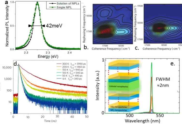
3.1. Narrow PL and fast lifetime
Colloidal NPLs exhibit three striking features compared to QDs : narrow optical feature, fast photoluminescence (PL) lifetime and almost no Stoke’s shift.61 At room temperature the ensemble emission spectrum is almost the same as at
the single particle one (Figure 5a). The FWHM at RT typically ranges from 7 to 10 nm, corresponding to a linewidth between 1 and 2 kbT. Contrary to QDs, NPLs present a thickness controlled at the atomic scale leading to a PL without
inhomogeneous broadening. This observation has been confirmed using 2D spectroscopy (Figure 5b, c).62 Compared
to 0D and 1D nanorods, NPLs present narrower PL signal along the diagonal (homogeneous broadening) and perpendicular to the diagonal (inhomogeneous broadening).
Figure 5 : (a) PL spectrum of a single CdSe NPL and of an assembly of them at room temperature. Reprinted with permission from ref 61. Copyright 2012 American Chemical Society. 2D electronic spectrum of colloidal spherical QDs (b) and NPLs (c). Reprinted with permission from ref 62. Copyright 2013, AIP Publishing LLC. (d) Time resolved PL spectra of CdSe NPLs at different temperature. Reprinted by permission from Macmillan Publishers Ltd. Nature Material in ref
25, copyright 2011. (d) Lasing signal of core shell NPLs integrated between two colloidally prepared Bragg mirrors, Adapted with permission from ref 63. Copyright (2014) American Chemical Society.
3.2. Nanoplatelets’ band structure
One of the main promises of NPLs is their 2D character. The band structure of NPLs has been modeled using different approaches: infinite well approximation,11 k·p modelling,25 Hartree renormalized k·p method,64 tight binding,42 or a
phenomenological spinning arrow moving in a box.65 These different models all attribute the first two excitonic
features to the heavy hole to electron and light hole to electron transitions (figure 2e).
Moreover, the facets of these platelets are capped with organic ligands, and the platelets are typically surrounded by solvents or by air. This means that carrier confinement and exciton binding energies are much stronger in colloidal nanoplatelets than in epitaxial QWs,42,64 which are buried in a crystal of a second semiconductor material. The strongly
bound character of the exciton in NPLs was then confirmed using time resolved spectroscopy method.66 One of the
consequences of this is an enhanced oscillator strength.25
Compared to 0D QDs, the PL lifetime is much faster in NPLs (Figure 5d).25,67 It is of a few nanoseconds at room
temperature going down by a decade to 300 ps at 4K. The dynamic of the exciton in the NPLs has also been tested using transient absorption. Pelton et al. concluded that the exciton indeed behaves as a 2D system. While optically charging the system, the authors observe first a bleach of the interband transition as well as the appearance of a new peak in the near infrared68 very likely related to some interband feature. The role of the phonon into NPL is not yet
completely clear since both fast68 and slow64 coupling to LO phonon has been claimed. Another striking feature related
to the assembly of nanoplatelets is the appearance of a second PL peak attributed to the phonon replica due to the higher phonon coupling in strongly packed NPL assemblies.69
3.3. ASE and lasing
The fast PL lifetime is extremely interesting from a light-emission perspective. In addition to the integration of NPLs into LED which is discussed in the next section, NPLs appear as candidates for stimulated emission and lasing. She et
al. and Guzelturk et al. respectively reported amplified spontaneous emission (ASE) properties from CdSe/CdS
core/shell70 and core/crown NPLs.63 In both cases a significant decrease of the power threshold for amplified
stimulated emission compared to QDs is observed (6µJ.cm-2 in the core/shell geometry) and the gain measured are
higher (≈ 600 cm-1 - at least 4 fold the one of QDs). This result also stands when performing two photons pumping.63
Reference 63 takes advantages of this large gain to integrate NPLs between two Bragg mirrors, which are also colloidally
prepared (Figure 5e, inset). The authors report a two photons pumped laser with a FWHM of 2 nm and a threshold of 2.5 mJ. cm-2.
4. Device
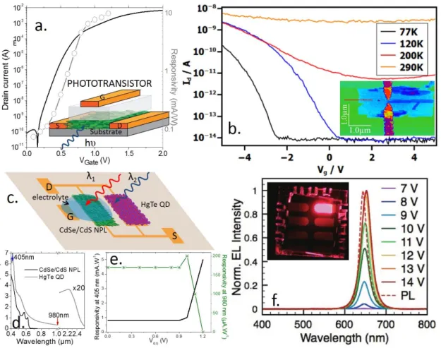
Integration of NPLs into optoelectronic devices71 has so far been less studied than their spectroscopic properties.
Nevertheless, NPLs offer some interesting perspectives for transport. In a film of CQDs, the transport is a hopping process where the carrier has to tunnel through the interparticle medium (i.e. the ligands). This process is responsible for the overall low mobility of CQD solid (10-6 cm2V-1s-1 with long ligands at the end of the synthesis to 1-10 cm2V-1s-1
while using ionic72-74 or metal chalcogenides ligands37). Thanks to their large lateral size, the number of hopping
processes requested to reach the electrodes is reduced while switching from QDs to NPLs. The transport in films of NPLs has been probed in a transistor configuration.75 The gating is ensured using ion gel electrolyte. The film made of
CdSe or CdSe/CdS NPLs presents a n-type character, while the CdTe NPLs are p-type. Our group obtain record on/off ratio above 108 on CdSe/CdS, while the subthreshold slope is 80mV/decade (Figure 6a).
Figure 6 : a) Transfer curve (drain current vs gate bias) for a film of CdSe/CdS NPLs gated with ion gel polymer. VDS is set at 0.5V and measurements are made at room temperature in air. The inset is a scheme of the device. b) Transfer curve for a transistor made of a single PbS NPL. The inset is an AFM image of the device, reprinted with permission from reference76. Copyright (2012), AIP Publishing LLC. c) Scheme of a bicolor detector made of a gated film of CdSe/CdS NPLs and HgTe CQDs. d) absorption spectrum for CdSe/CdS NPLs and for HgTe CQDs. e) Responsivity at 405 nm and 980 nm as a function of gate bias for the device of part c. Adapted from reference 77, Copyright 2014 American Chemical Society f) Electroluminescence spectra of CdSe/CdS NPLs under different biases. The inset is a picture of the device under operation. Adapted from reference78, copyright 2013 WILEY-VCH Verlag GmbH.
A key advantage of NPLs compared to 0D structures is their potentially stronger compatibility with usual technological processes thanks to their large lateral size. While for CQDs, the connection of the particles at the single particle remains tricky,79 NPLs are the right candidate to connect a single particle using a top down approach. It consequently becomes
reasonable to connect using usual e-beam lithography process a single particle, as it is commonly done for graphene sheet or metal dichalcogenides. Klinke’s group reported transistor and detector obtained by the connection of a single PbS nanosheet (Figure 6b).76 Almost no gate effect is achieved at room temperature, consistent with the narrow band
gap nature of the PbS nanosheets. On the other hand, large current modulations (on/off ratio of 105) are obtained at
low temperature. One of the key advantages of these micrometer scale nanosheets compared to 0D objects is their large absorption cross section which allows a large current modulation under illumination even on a single particle. Films of NPL also present some photoconductive behavior, but with poor photoresponse (tens of µA.W-1). One of the
possible reasons for such low responsivity is the strong exciton binding energy of NPLs. Typically, for 10 V applied over 10 µm spaced electrodes the potential drop per NPL is around tens meV,not enough to dissociate the electron/hole pair with a binding energy higher than 200 meV.42,64 A possible way to enhance the photoresponse of the NPLs film is
to gate the film using ion gel electrolyte. By raising the Fermi level just below the conduction band, the trap states are filled and the photoactivated carriers can no longer get trapped. The gating leads to an increased photocarrier lifetime and finally to a rise of the photoresponse up to three decades (Figure 6a). This gated film of NPLs was also used to build the first bicolor detector77 based only on colloidal nanocrystals (Figure 6c). The device relies on two materials:
6d). By switching the gate bias the authors demonstrated that the spectral range of one material or the other can be activated (Figure 6e).
Another interesting aspect of the use of nanoplatelets for optoelectronic devices is the fine control of the optical features. The narrow PL linewidth of the CdSe cores (FWHM ≈ 10 nm) and CdSe/CdS core/shells (FWHM ≈ 20 nm) can be used to build LEDs with narrow electroluminescence emission. Such narrowness is motivated by the idea to obtain LED-based devices with an improved color gamut. CdSe/CdZnS NPLs have been integrated in a p-n junction where ZnO nanocrystals are used as the n-layer and PEDOT-PVK as the hole-transport layer.80 The electroluminescence signal
overlaps nicely with the PL signal with no additional broadening (Figure 6f). As the bias of the sample is increased, a redshift of the transition is observed attributed to the Stark effect.81
CONCLUSION
In this review some of the recent results related to metal chalcogenides 2D colloidal nanoplatelets are discussed. Atomic control of the growth can be obtained thanks to a careful control of the ligands capping the different facets of a seed. Core/shell as well as core/crown heterostructures can be synthesized. The lack of inhomogeneous broadening allows reaching PL features which are so far inaccessible to spherical QDs. Spectroscopic measurements have confirmed the 2D character of the NPLs in a band structure and charge carrier dynamic point of view. NPLs appear as very promising candidates for lasing since very low power threshold has been reported. Integration of NPLs into devices has led to very promising performance for phototransistor and single particle electronics.
Acknowledgements
The authors thank Xiang Zhen Xu for her help with TEM imaging. BD thanks Agence National de la Recherche for funding through grants SNAP and QDOTICS. This work has been supported by the Region Ile-de-France in the framework of DIM Nano-K.
Biographies
Emmanuel Lhuillier was undergraduate at ESPCI and got his PhD from Ecole Polytechnique (France) for his work on transport in weakly coupled superlattice under the supervision of Emmanuel Rosencher. He then moved to university of Chicago in the Guyot-Sionnest’s group where he worked on infrared photodetection using colloidal nanocrystals. He then joined Nexdot where he is in charge of the optoelectronic devices development. His interest deals with the study of transport and phototransport in low dimensional colloidal semiconductor.
Silvia Pedetti is currently a PhD student at the Laboratoire de Physique et d’Etude des Matériaux in Paris. She received her MSc in organic chemistry from the Università La Sapienza in 2011. Her research focuses on the synthesis and characterization of 2-dimensional chalcogenides semiconductors nanocrystals.
Sandrine Ithurria is a former undergraduate student from ESPCI in Paris, she joined the Dubertret’s group in 2007 for her PhD where she developed the synthesis of the 2D Cadmium chalcogenides nanoplatelets. In 2010 she joined the Talapin’s group at The university of Chicago for her post doc, where she worked on low temperature growth method of colloidal nanocrystals. Since 2012 she is assistant professor at ESPCI. Her research field is focused on colloidal nanocrystal syntheses and functionalizations.
Brice Nadal received his engineer’s degree from CPE Lyon in 2006. He obtained his PhD degree from the University Paris Sud in 2009. Then He did postdoctoral research at the enginnering school ESPCI ParisTech with Dr Benoit Dubertret and Dr Hervé Aubin from January 2010 to June 2011. He is currently working at Nexdot. His interests include the synthesis, characterization and mechanistic investigation of organic and inorganic materials.
Hadrien Heuclin Hadrien Heuclin did his undergraduate studies at the Ecole Polytechnique from 2005 to 2009. He then completed his PhD at the Ecole Polytechnique under the supervision of Dr. Nicolas Mézailles in October 2012. His
research interests focused on the use of germinal dianions as precursors for the synthesis of transition metal carbene complexes. He joined Nexdot where his work addresses the synthesis and characterization of innovative 2D materials. Benoit Dubertret received his PhD from the University Louis Pasteur in Strasbourg, France in 1998 and made a post doc at The Rockfeller University in the group of Albert Libchaber. He is a CNRS researcher, group leader of the quantum dot team in the LPEM laboratory at ESPCI. His team is a 25 persons group with interest in nanoparticle synthesis, bio application, visible optical spectroscopy and device application. Benoit is the author of ≈100 papers and 6 patents or patent applications. He is married and has 7 children.
REFERENCES
(1) Rogach, A. Quantum Dots Still Shining Strong 30 Years On. ACS Nano 2014, 8, 6511-6512.
(2) Ekimov, A. I.; Onushchenko, A. A. Quantum Size Effect in 3-Dimensional Microscopic Semiconductor Crystals. Jetp Lett. 1981, 34, 345-349.
(3) Efros, A. L.; Efros, A. L. Interband Absorption of Light in a Semiconductor Sphere. Soviet Physics
Semiconductors-Ussr 1982, 16, 772-775.
(4) Brus, L. E. A Simple-Model for the Ionization-Potential, Electron-Affinity, and Aqueous Redox Potentials of Small Semiconductor Crystallites. J Chem Phys 1983, 79, 5566-5571.
(5) Murray, C. B.; Norris, D. J.; Bawendi, M. G. Synthesis and Characterization of Nearly Monodisperse Cde (E = S, Se, Te) Semiconductor Nanocrystallites. J Am Chem Soc 1993, 115, 8706-8715.
(6) Michalet, X.; Pinaud, F. F.; Bentolila, L. A.; Tsay, J. M.; Doose, S.; Li, J. J.; Sundaresan, G.; Wu, A. M.; Gambhir, S. S.; Weiss, S. Quantum dots for live cells, in vivo imaging, and diagnostics. Science 2005, 307, 538-544.
(7) Reiss, P.; Protiere, M.; Li, L. Core/Shell Semiconductor Nanocrystals. Small 2009, 5, 154-168.
(8) Yin, Y.; Alivisatos, A. P. Colloidal nanocrystal synthesis and the organic-inorganic interface. Nature 2005, 437, 664-670.
(9) Peng, X. G.; Manna, L.; Yang, W. D.; Wickham, J.; Scher, E.; Kadavanich, A.; Alivisatos, A. P. Shape control of CdSe nanocrystals. Nature 2000, 404, 59-61.
(10) Yu, H.; Li, J. B.; Loomis, R. A.; Gibbons, P. C.; Wang, L. W.; Buhro, W. E. Cadmium selenide quantum wires and the transition from 3D to 2D confinement. J Am Chem Soc 2003, 125, 16168-16169.
(11) Ithurria, S.; Dubertret, B. Quasi 2D Colloidal CdSe Platelets with Thicknesses Controlled at the Atomic Level. J Am Chem Soc 2008, 130, 16504-16505.
(12) Chhowalla, M.; Shin, H. S.; Eda, G.; Li, L. J.; Loh, K. P.; Zhang, H. The chemistry of two-dimensional layered transition metal dichalcogenide nanosheets. Nat. Chem. 2013, 5, 263-275.
(13) Bouet, C.; Tessier, M. D.; Ithurria, S.; Mahler, B.; Nadal, B.; Dubertret, B. Flat Colloidal Semiconductor Nanoplatelets. Chem Mater 2013, 25, 1262-1271.
(14) Yang, J.; Son, J. S.; Yu, J. H.; Joo, J.; Hyeon, T. Advances in the Colloidal Synthesis of Two-Dimensional Semiconductor Nanoribbons. Chem Mater 2013.
(15) Joo, J.; Son, J. S.; Kwon, S. G.; Yu, J. H.; Hyeon, T. Low-temperature solution-phase synthesis of quantum well structured CdSe nanoribbons. J Am Chem Soc 2006, 128, 5632-5633.
(16) Son, J. S.; Park, K.; Kwon, S. G.; Yang, J.; Choi, M. K.; Kim, J.; Yu, J. H.; Joo, J.; Hyeon, T. Dimension-Controlled Synthesis of CdS Nanocrystals: From 0D Quantum Dots to 2D Nanoplates. Small 2012, 8, 2394-2402.
(17) Son, J. S.; Yu, J. H.; Kwon, S. G.; Lee, J.; Joo, J.; Hyeon, T. Colloidal Synthesis of Ultrathin Two-Dimensional Semiconductor Nanocrystals. Adv Mater 2011, 23, 3214-3219.
(18) Yu, J. H.; Liu, X. Y.; Kweon, K. E.; Joo, J.; Park, J.; Ko, K. T.; Lee, D.; Shen, S. P.; Tivakornsasithorn, K.; Son, J. S.; Park, J. H.; Kim, Y. W.; Hwang, G. S.; Dobrowolska, M.; Furdyna, J. K.; Hyeon, T. Giant Zeeman splitting in nucleation-controlled doped CdSe:Mn2+ quantum nanoribbons. Nature Materials 2010, 9, 47-53.
(19) Son, J. S.; Wen, X. D.; Joo, J.; Chae, J.; Baek, S. I.; Park, K.; Kim, J. H.; An, K.; Yu, J. H.; Kwon, S. G.; Choi, S. H.; Wang, Z. W.; Kim, Y. W.; Kuk, Y.; Hoffmann, R.; Hyeon, T. Large-Scale Soft Colloidal Template Synthesis of 1.4 nm Thick CdSe Nanosheets. Angew Chem Int Edit 2009, 48, 6861-6864.
(20) Liu, Y. H.; Wang, F. D.; Wang, Y. Y.; Gibbons, P. C.; Buhro, W. E. Lamellar Assembly of Cadmium Selenide Nanoclusters into Quantum Belts. J Am Chem Soc 2011, 133, 17005-17013.
(21) Wang, Y. Y.; Liu, Y. H.; Zhang, Y.; Wang, F. D.; Kowalski, P. J.; Rohrs, H. W.; Loomis, R. A.; Gross, M. L.; Buhro, W. E. Isolation of the Magic-Size CdSe Nanoclusters (CdSe)13(n-octylamine)13 and (CdSe)13(oleylamine)13.
(22) Wang, Y. Y.; Zhang, Y.; Wang, F. D.; Giblin, D. E.; Hoy, J.; Rohrs, H. W.; Loomis, R. A.; Buhro, W. E. The Magic-Size Nanocluster (CdSe)(34) as a Low-Temperature Nucleant for Cadmium Selenide Nanocrystals; Room-Temperature Growth of Crystalline Quantum Platelets. Chem Mater 2014, 26, 2233-2243.
(23) Schliehe, C.; Juarez, B. H.; Pelletier, M.; Jander, S.; Greshnykh, D.; Nagel, M.; Meyer, A.; Foerster, S.; Kornowski, A.; Klinke, C.; Weller, H. Ultrathin PbS Sheets by Two-Dimensional Oriented Attachment. Science 2010, 329, 550-553.
(24) Ithurria, S.; Bousquet, G.; Dubertret, B. Continuous Transition from 3D to 1D Confinement Observed during the Formation of CdSe Nanoplatelets. J Am Chem Soc 2011, 133, 3070-3077.
(25) Ithurria, S.; Tessier, M. D.; Mahler, B.; Lobo, R. P.; Dubertret, B.; Efros, A. L. Colloidal nanoplatelets with two-dimensional electronic structure. Nat Mater 2011, 10, 936-941.
(26) Bastard, G.; Mendez, E. E.; Chang, L. L.; Esaki, L. Exciton Binding-Energy in Quantum Wells. Phys Rev B 1982, 26, 1974-1979.
(27) Bouet, C.; Mahler, B.; Nadal, B.; Abecassis, B.; Tessier, M. D.; Ithurria, S.; Xu, X. Z.; Dubertret, B. Two-Dimensional Growth of CdSe Nanocrystals, from Nanoplatelets to Nanosheets. Chem Mater 2013, 25, 639-645.
(28) Pedetti, S.; Nadal, B.; Lhuillier, E.; Mahler, B.; Bouet, C.; Abecassis, B.; Xu, X. Z.; Dubertret, B. Optimized Synthesis of CdTe Nanoplatelets and Photoresponse of CdTe Nanoplatelets Films. Chem Mater 2013, 25, 2455-2462.
(29) Li, Z.; Peng, X. G. Size/Shape-Controlled Synthesis of Colloidal CdSe Quantum Disks: Ligand and Temperature Effects. J Am Chem Soc 2011, 133, 6578-6586.
(30) Mahler, B.; Spinicelli, P.; Buil, S.; Quelin, X.; Hermier, J. P.; Dubertret, B. Towards non-blinking colloidal quantum dots. Nature Materials 2008, 7, 659-664.
(31) Hines, M. A.; Guyot-Sionnest, P. Bright UV-blue luminescent colloidal ZnSe nanocrystals. J Phys Chem
B 1998, 102, 3655-3657.
(32) Manna, L.; Scher, E. C.; Li, L. S.; Alivisatos, A. P. Epitaxial growth and photochemical annealing of graded CdS/ZnS shells on colloidal CdSe nanorods. J Am Chem Soc 2002, 124, 7136-7145.
(33) Donega, C. D. Synthesis and properties of colloidal heteronanocrystals. Chem. Soc. Rev. 2011, 40, 1512-1546.
(34) Mahler, B.; Nadal, B.; Bouet, C.; Patriarche, G.; Dubertret, B. Core/shell colloidal semiconductor nanoplatelets. J Am Chem Soc 2012, 134, 18591-18598.
(35) Ithurria, S.; Talapin, D. V. Colloidal atomic layer deposition (c-ALD) using self-limiting reactions at nanocrystal surface coupled to phase transfer between polar and nonpolar media. J Am Chem Soc 2012, 134, 18585-18590.
(36) Nag, A.; Kovalenko, M. V.; Lee, J. S.; Liu, W. Y.; Spokoyny, B.; Talapin, D. V. Metal-free Inorganic Ligands for Colloidal Nanocrystals: S(2-), HS(-), Se(2-), HSe(-), Te(2-), HTe(-), TeS(3)(2-), OH(-), and NH(2)(-) as Surface Ligands.
J Am Chem Soc 2011, 133, 10612-10620.
(37) Kovalenko, M. V.; Scheele, M.; Talapin, D. V. Colloidal Nanocrystals with Molecular Metal Chalcogenide Surface Ligands. Science 2009, 324, 1417-1420.
(38) Thomson, J. W. T. J. W.; Nagashima, K.; Macdonald, P. M.; Ozin, G. A. From Sulfur-Amine Solutions to Metal Sulfide Nanocrystals: Peering into the Oleylamine-Sulfur Black Box. J Am Chem Soc 2011, 133, 5036-5041.
(39) Tessier, M. D.; Mahler, B.; Nadal, B.; Heuclin, H.; Pedetti, S.; Dubertret, B. Spectroscopy of Colloidal Semiconductor Core/Shell Nanoplatelets with High Quantum Yield. Nano Letters 2013, 13, 3321-3328.
(40) Prudnikau, A.; Chuvilin, A.; Artemyev, M. CdSe-CdS Nanoheteroplatelets With Efficient Photoexcitation of Central CdSe Region through Epitaxially Grown CdS Wings. J Am Chem Soc 2013, 135, 14476-14479.
(41) Tessier, M. D.; Spinicelli, P.; Dupont, D.; Patriarche, G.; Ithurria, S.; Dubertret, B. Efficient Exciton Concentrators Built from Colloidal Core/Crown CdSe/CdS Semiconductor Nanoplatelets. Nano Letters 2014, 14, 207-213.
(42) Benchamekh, R.; Gippius, N. A.; Even, J.; Nestoklon, M. O.; Jancu, J. M.; Ithurria, S.; Dubertret, B.; Efros, A.; Voisin, P. Tight-binding calculations of image-charge effects in colloidal nanoscale platelets of CdSe. Phys Rev B 2014, 89, 7.
(43) Pedetti, S.; Ithurria, S.; Heuclin, H.; Patriarche, G.; Dubertret, B. Type-II CdSe/CdTe Core/Crown Semiconductor Nanoplatelets. J Am Chem Soc 2014.
(44) Son, D. H.; Hughes, S. M.; Yin, Y. D.; Alivisatos, A. P. Cation exchange reactions-in ionic nanocrystals.
Science 2004, 306, 1009-1012.
(45) Li, H. B.; Zanella, M.; Genovese, A.; Povia, M.; Falqui, A.; Giannini, C.; Manna, L. Sequential Cation Exchange in Nanocrystals: Preservation of Crystal Phase and Formation of Metastable Phases. Nano Letters 2011, 11, 4964-4970.
(46) Beberwyck, B. J.; Surendranath, Y.; Alivisatos, A. P. Cation Exchange: A Versatile Tool for Nanomaterials Synthesis. J. Phys. Chem. C 2013, 117, 19759-19770.
(47) Li, H.; Brescia, R.; Krahne, R.; Bertoni, G.; Alcocer, M. J. P.; D'Andrea, C.; Scotognella, F.; Tassone, F.; Zanella, M.; De Giorgi, M.; Manna, L. Blue-UV-Emitting ZnSe(Dot)/ZnS(Rod) Core/Shell Nanocrystals Prepared from CdSe/CdS Nanocrystals by Sequential Cation Exchange. ACS Nano 2012, 6, 1637-1647.
(48) Li, H.; Brescia, R.; Povia, M.; Prato, M.; Bertoni, G.; Manna, L.; Moreels, I. Synthesis of uniform disk-shaped copper telluride nanocrystals and cation exchange to cadmium telluride quantum disks with stable red emission. J Am Chem Soc 2013, 135, 12270-12278.
(49) Yang, X.; Xue, H. T.; Xu, J.; Huang, X.; Zhang, J.; Tang, Y. B.; Ng, T. W.; Kwong, H. L.; Meng, X. M.; Lee, C. S. Synthesis of Porous ZnS:Ag2S Nanosheets by Ion Exchange for Photocatalytic H-2 Generation. ACS Appl. Mater.
Interfaces 2014, 6, 9078-9084.
(50) Bouet, C.; Laufer, D.; Mahler, B.; Nadal, B.; Heuclin, H.; Pedetti, S.; Patriarche, G.; Dubertret, B. Synthesis of Zinc and Lead Chalcogenide Core and Core/Shell Nanoplatelets Using Sequential Cation Exchange Reactions. Chem Mater 2014, 26, 3002-3008.
(51) Lesnyak, V.; George, C.; Genovese, A.; Prato, M.; Casu, A.; Ayyappan, S.; Scarpellini, A.; Manna, L. Alloyed Copper Chalcogenide Nanoplatelets via Partial Cation Exchange Reactions. ACS Nano 2014, 8, 8407-8818.
(52) Glotzer, S. C.; Solomon, M. J. Anisotropy of building blocks and their assembly into complex structures.
Nature Materials 2007, 6, 557-562.
(53) Nie, Z. H.; Petukhova, A.; Kumacheva, E. Properties and emerging applications of self-assembled structures made from inorganic nanoparticles. Nat. Nanotechnol. 2010, 5, 15-25.
(54) Saunders, A. E.; Ghezelbash, A.; Smilgies, D. M.; Sigman, M. B.; Korgel, B. A. Columnar self-assembly of colloidal nanodisks. Nano Letters 2006, 6, 2959-2963.
(55) Du, X. S.; Mo, M. S.; Zheng, R. K.; Lim, S. H.; Meng, Y. Z.; Mai, Y. W. Shape-controlled synthesis and assembly of copper sulfide nanoparticles. Cryst. Growth Des. 2008, 8, 2032-2035.
(56) Li, X. M.; Shen, H. B.; Niu, J. Z.; Zhang, Y. G.; Wang, H. Z.; Li, L. S. Columnar Self-Assembly of Cu2S Hexagonal Nanoplates Induced by Tin(IV)-X Complex as Inorganic Surface Ligand. J Am Chem Soc 2010, 132, 12778-12779.
(57) Paik, T.; Ko, D. K.; Gordon, T. R.; Doan-Nguyen, V.; Murray, C. B. Studies of Liquid Crystalline Self-Assembly of GdF(3) Nanoplates by In-Plane, Out-of-Plane SAXS. ACS Nano 2011, 5, 8322-8330.
(58) Ye, X.; Chen, J.; Engel, M.; Millan, J. A.; Li, W.; Qi, L.; Xing, G.; Collins, J. E.; Kagan, C. R.; Li, J.; Glotzer, S. C.; Murray, C. B. Competition of shape and interaction patchiness for self-assembling nanoplates. Nat Chem 2013, 5, 466-473.
(59) Abecassis, B.; Tessier, M. D.; Davidson, P.; Dubertret, B. Self-Assembly of CdSe Nanoplatelets into Giant Micrometer-Scale Needles Emitting Polarized Light. Nano Letters 2014, 14, 710-715.
(60) Lhuillier, E.; Hease, P.; Ithurria, S.; Dubertret, B. Selective Electrophoretic Deposition of CdSe Nanoplatelets. Chem Mater 2014, 26, 4514-4520.
(61) Tessier, M. D.; Javaux, C.; Maksimovic, I.; Loriette, V.; Dubertret, B. Spectroscopy of Single CdSe Nanoplatelets. ACS Nano 2012, 6, 6751-6758.
(62) Griffin, G. B.; Ithurria, S.; Dolzhnikov, D. S.; Linkin, A.; Talapin, D. V.; Engel, G. S. Two-dimensional electronic spectroscopy of CdSe nanoparticles at very low pulse power. J Chem Phys 2013, 138.
(63) Guzelturk, B.; Kelestemur, Y.; Olutas, M.; Delikanli, S.; Demir, H. V. Amplified Spontaneous Emission and Lasing in Colloidal Nanoplatelets. ACS Nano 2014, 8, 6599-6605.
(64) Achtstein, A. W.; Schliwa, A.; Prudnikau, A.; Hardzei, M.; Artemyev, M. V.; Thomsen, C.; Woggon, U. Electronic Structure and Exciton-Phonon Interaction in Two-Dimensional Colloidal CdSe Nanosheets. Nano Letters 2012, 12, 3151-3157.
(65) Dijksman, A. T.; Dubertret, B. Accurate energy- size dependence of excitonic transitions in semiconductor nanocrystals and nanoplatelets using a phase jump approach. Phys. Status Solidi B-Basic Solid State
Phys. 2014, 251, 537-541.
(66) Kunneman, L. T.; Tessier, M. D.; Heuclin, H.; Dubertret, B.; Aulin, Y. V.; Grozema, F. C.; Schins, J. M.; Siebbeles, L. D. A. Bimolecular Auger Recombination of Electron-Hole Pairs in Two-Dimensional CdSe and CdSe/CdZnS Core/Shell Nanoplatelets. J. Phys. Chem. Lett. 2013, 4, 3574-3578.
(67) Biadala, L.; Liu, F.; Tessier, M. D.; Yakovlev, D. R.; Dubertret, B.; Bayer, M. Recombination Dynamics of Band Edge Excitons in Quasi-Two-Dimensional CdSe Nanoplatelets. Nano Letters 2014, 14, 1134-1139.
(68) Pelton, M.; Ithurria, S.; Schaller, R. D.; Dolzhnikov, D. S.; Talapin, D. V. Carrier cooling in colloidal quantum wells. Nano Lett 2012, 12, 6158-6163.
(69) Tessier, M. D.; Biadala, L.; Bouet, C.; Ithurria, S.; Abecassis, B.; Dubertret, B. Phonon Line Emission Revealed by Self-Assembly of Colloidal Nanoplatelets. ACS Nano 2013, 7, 3332-3340.
(70) She, C. X.; Fedin, I.; Dolzhnikov, D. S.; Demortiere, A.; Schaller, R. D.; Pelton, M.; Talapin, D. V. Low-Threshold Stimulated Emission Using Colloidal Quantum Wells. Nano Letters 2014, 14, 2772-2777.
(71) Talapin, D. V.; Lee, J. S.; Kovalenko, M. V.; Shevchenko, E. V. Prospects of Colloidal Nanocrystals for Electronic and Optoelectronic Applications. Chem. Rev. 2010, 110, 389-458.
(72) Nag, A.; Chung, D. S.; Dolzhnikov, D. S.; Dimitrijevic, N. M.; Chattopadhyay, S.; Shibata, T.; Talapin, D. V. Effect of Metal Ions on Photoluminescence, Charge Transport, Magnetic and Catalytic Properties of All-Inorganic Colloidal Nanocrystals and Nanocrystal Solids. J Am Chem Soc 2012, 134, 13604-13615.
(73) Tang, J.; Kemp, K. W.; Hoogland, S.; Jeong, K. S.; Liu, H.; Levina, L.; Furukawa, M.; Wang, X. H.; Debnath, R.; Cha, D. K.; Chou, K. W.; Fischer, A.; Amassian, A.; Asbury, J. B.; Sargent, E. H. Colloidal-quantum-dot photovoltaics using atomic-ligand passivation. Nature Materials 2011, 10, 765-771.
(74) Koh, W. K.; Saudari, S. R.; Fafarman, A. T.; Kagan, C. R.; Murray, C. B. Thiocyanate-Capped PbS Nanocubes: Ambipolar Transport Enables Quantum Dot Based Circuits on a Flexible Substrate. Nano Letters 2011, 11, 4764-4767.
(75) Lhuillier, E.; Pedetti, S.; Ithurria, S.; Heuclin, H.; Nadal, B.; Robin, A.; Patriarche, G.; Lequeux, N.; Dubertret, B. Electrolyte-Gated Field Effect Transistor to Probe the Surface Defects and Morphology in Films of Thick CdSe Colloidal Nanoplatelets. ACS Nano 2014, 8, 3813-3820.
(76) Dogan, S.; Bielewicz, T.; Cai, Y. X.; Klinke, C. Field-effect transistors made of individual colloidal PbS nanosheets. Appl Phys Lett 2012, 101, 4.
(77) Lhuillier, E.; Robin, A.; Ithurria, S.; Aubin, H.; Dubertret, B. Electrolyte-Gated Colloidal Nanoplatelets-Based Phototransistor and Its Use for Bicolor Detection. Nano Letters 2014, 14, 2715-2719.
(78) Chen, Z. Y.; Nadal, B.; Mahler, B.; Aubin, H.; Dubertret, B. Quasi-2D Colloidal Semiconductor Nanoplatelets for Narrow Electroluminescence. Adv. Funct. Mater. 2014, 24, 295-302.
(79) Yu, Q.; Cui, L. M.; Lequeux, N.; Zimmers, A.; Ulysse, C.; Rebuttini, V.; Pinna, N.; Aubin, H. In-Vacuum Projection of Nanoparticles for On-Chip Tunneling Spectroscopy. ACS Nano 2013, 7, 1487-1494.
(80) Chen, Z.; Nadal, B.; Mahler, B.; Aubin, H.; Dubertret, B. Quasi-2D Colloidal Semiconductor Nanoplatelets for Narrow Electroluminescence. Adv. Funct. Mater. 2013.