HAL Id: tel-00288338
https://tel.archives-ouvertes.fr/tel-00288338
Submitted on 16 Jun 2008HAL is a multi-disciplinary open access archive for the deposit and dissemination of sci-entific research documents, whether they are pub-lished or not. The documents may come from teaching and research institutions in France or abroad, or from public or private research centers.
L’archive ouverte pluridisciplinaire HAL, est destinée au dépôt et à la diffusion de documents scientifiques de niveau recherche, publiés ou non, émanant des établissements d’enseignement et de recherche français ou étrangers, des laboratoires publics ou privés.
Optical and vibrational properties of new
”Nano-Designed” materials produced by pulsed laser
deposition
Jeremie Margueritat
To cite this version:
Jeremie Margueritat. Optical and vibrational properties of new ”Nano-Designed” materials produced by pulsed laser deposition. Physics [physics]. Université Paul Sabatier - Toulouse III, 2008. English. �tel-00288338�
Optical and vibrational properties of new
“Nano-Designed” materials produced by
pulsed laser deposition
by J´er´emie Margueritat
under the supervision of
Jose Gonzalo de los Reyes & Adnen Mlayah A Thesis submitted to the
Universidad Autonoma de Madrid & Universit´e Paul Sabatier, Toulouse III for the obtention of the
Degree of Doctor in Philosophy speciality :
“F´ısica de Materiales” and “Nanophysique, Nanomesures et Nanocomposants”
before a Jury composed by : Jos´e Garc´ıa Sol´e (President) Fco. Javier Sol´ıs C´espedes (Referee)
Bruno Palpant (Referee) Fco. Jos´e Garc´ıa Vidal
Adnen Mlayah
LPG
Instituto de ´Optica
CSIC Madrid, April 2008
CEMES Universit´e Paul Sabatier CNRS
The physical properties of a metal object change when its charcteristic size is reduced down to few nanometers. This is related to the quantum confinement of electronic states and to the importance of surface excitations in small objects. The combination of these effects with those derived from its inclusion in a host matrix allows the design of new materials with special macroscopic properties. Thus, the control of the size and shape of embedded structures within a few nanometers is one of the most challenging issues faced by nanoscience. In particular, noble metal nanoparticles (NPs) embedded in a dielectric matrix have widely been studied in recent years, since their unique optical properties make them promising materials for optical applications if a good control over the spectral response is achieved. This work focuses on the particular case of thin amorphous Al2O3
(a-Al2O3) films containing nano-designed Ag nanostructures. The optical properties of
Ag nanostructures are characterized by the absorption at the surface plasmon resonance (SPR) wavelength that depends on the nanoparticles morphology. Further tuning of the SPR can be achieved through the synthesis of ordered nanoparticles with complex shapes and controlled morphology. This possibility is particularly challenging, since new optical properties should arise from this “nano-design”.
Among the possible ways to control the morphology, we have developed a new route to produce thin films containing such shaped nanoparticles, based on the alternate pulsed laser deposition (a-PLD) technique, which allows the deposition of multilayered thin films, offers an excellent control of deposition sequence, and in the case of nanoparti-cles, allows partial control of the nanoparticles morphology. Using this route we have produced nanostructured thin films containing spherical Ag nanoparticles, nanolentils or nanocolumns, to study the relationship between morphology and optical properties, as well as mixed structures containing alternate layers of Co and Ag nanoparticles to study the plasmon-vibration interaction regime.
The morphology of the nanostructured thin films has been studied using transmission electron microscopy (TEM). The analysis of plan-view and cross section images has shown that we were able to produce spherical Ag nanoparticles with diameters in the range from 2 to 5 nm, nanolentils with an average in-plane diameter of 10 nm and an average height of 6 nm and finally, nanocolumns with average diameters in the range from 2 to 3 nm and a height that as been varied from 6.5 to 65 nm, which corresponds to aspect ratios from 0.6 to 25. Nevertheless, some discontinuities have been observed in the case of nanocolumns, that are most likely related to the production procedure. In the case of samples containing Co and Ag nanoparticles, TEM images show the formation of layers containing spherical Co nanoparticles with an average diameter of 2.7 nm and
iv
Ag nanolentils with an average diameter of 10 nm and an average height of 6 nm. The in-depth sparation between the layers of Co and Ag NPs has been varied from 4 to 8 nm.
The optical properties of these nanostructures have been studied using optical ab-sorption spectra and low frequency Raman spectroscopy. The presence of non-spherical Ag nanoparticles is evidenced in the optical absorption spectrum through the presence of two surface plasmon resonances, the longitudinal and transverse SPR. When the aspect ratio is larger than 1 (nanocolumns) these SPR are located respectively at higher and lower wavelength than that of spherical nanoparticles, while for aspect ratios smaller than 1 (nanolentils) the opposite occurs. Moreover, the well defined longitudinal and transverse SPR modes confirm the self-orientation perpendicular to the substrate surface in the case of the nanocolumns. These results are confirmed by the confined acoustic vi-bration bands observed in the Raman spectra. In the case of spherical nanoparticles the band observed is due to the degenerated quadrupolar vibration mode (l = 2; m =±0,1,2;
n = 0). When the aspect ratio differs from 1 the five fold of the quadrupolar vibration
mode are not longer degenerated and the frequency of the band observed is shifted with respect to the case of spherical nanoparticles. The vibrations modes observed for sam-ples containing nanolentils or nanocolumns have been identified as spheroidal-like modes (l = 2; m =±0,1; n = 0) and (l = 2; m = ±2; n = 0), respectively.
The final part of the work is devoted to the study of the Raman response of samples containing Co nanoparticles and Ag nanolentils. Raman scattering, of samples con-taining only Ag nanolentils, excited at a wavelength close to the SPR reveals confined acoustic phonons of the silver nanolentils, while no vibration bands were observed in samples containing only Co nanoparticles. In mixed systems the vibration band cor-responding to Ag nanolentils remains constant, while a new band related to acoustic vibrations of Co nanoparticles appears when the distance between Co nanoparticles and Ag nanolentils layers decreases below a certain threshold. The analysis of the Ra-man scattering suggests the existence of coupling between Co and Ag nanoparticles for separations shorter than 6 nm that is most likely related to the interaction of the Co quadrupolar acoustic vibrations with the electric field generated by the SPR of the Ag nanolentils.
The experimental results presented have also been compared to theory, which has al-lowed relating the morphology of the nanostructures with their optical properties, and at the same time, studying different couplings: plasmon-plasmon (between nanocolumns) and plasmon-vibration in the samples containing either Ag nanocolumns or Co and Ag
v layers of nanoparticles and nanolentils, respectively.
vi
Spanish abstract
Se han desarrollado nuevos conceptos de fabricaci´on de materiales nanoestructurados en l´amina delgada basados en el dep´osito por l´aser pulsado alterno de un metal (Ag) y un diel´ectrico (Al2O3), que han permitido alcanzar un control ´optimo sobre los par´ametros
morfol´ogicos de las nanoestructuras que determinan su respuesta ´optica. Se han pro-ducido nanoesferas, “nanolentils” y nanocolumnas auto-ensambladas orientadas. Se ha correlacionado su respuesta ´optica lineal con su morfolog´ıa y se ha simulado la respuesta ´optica utilizando diferentes modelos te´oricos. En paralelo al estudio ´optico, se ha anal-izado la respuesta vibracional de las nanoestructuras mediante dispersi´on Raman de baja frecuencia. Por ´ultimo, se han fabricado nanoestructuras que contienen capas alternas de nanopart´ıculas de Co y de Ag separadas por una distancia de unos pocos nanometros, en las que se ha observado que la interacci´on entre el plasmon superficial y los modos vibracionales esferoidales de las nanopart´ıculas activa la se˜nal Raman.
French abstract
Nous avons d´evelopp´e de nouveaux concepts de fabrication de mat´eriaux nanostruc-tur´es en couche mince bas´es sur le d´epˆot par ablation laser altern´e d’un m´etal (Ag) et d’un di´electrique (Al2O3). Cette technique permet d’atteindre un contrˆole optimal
sur les param`etres morphologiques des nanostructures qui d´eterminent la r´eponse op-tique des couches minces. Nous avons produit des nanosph`eres, des ”nanolentils” et des nanocolonnes, auto-organis´ees et orient´ees, encapsul´ees dans une matrice d’alumine amorphe. Leur r´eponse optique a ´et´e ´etudi´ee en fonction de leur morphologie et com-par´ee ´a des simulations th´eoriques. En parall`ele ´a cette ´etude, la r´eponse vibrationnelle des nanostructures a ´et´e analys´ee par spectrom´etrie Raman basse fr´equence. Finale-ment, des nanostructures contenant des couches altern´ees de nanoparticules de Co et d’Ag s´epar´ees par une distance de quelques nanom`etres ont aussi ´et´e fabriqu´ees. Il a ´et´e montr´e que l’interaction entre le plasmon de surface et les modes sph´ero¨ıdaux de vibration des nanoparticules active le signal Raman.
vii
Acknowledgements
I express my deepest and sincere gratitude to my supervisors Prof. Adnen Mlayah and Dr. Jose Gonzalo (Pepe). Adnen helped me to find this opportunity in Madrid which has been a very good experience. That would have probably not been the case without Pepe, he welcomed me, and helped me to accommodate to the new life that was waiting me in Madrid. By telephone, e-mail or in live they constantly support, guide, and encourage me, giving me freedom and confidence necessary for doing innovative research. The numerous discussion about physics or life have made me a better and confident person. I am grateful to them for giving me the impetus for completing the research experiments and writing this thesis.
It is a privilege to thank Prof. Carmen N. Afonso for her collaboration to my work, discussing my results and their interpretations, and for her criticisms and compliments that helped me to improving my skills of researcher. I have benefited from her expertise of researcher and learn a lot from her great capacity to communicate scientific results.
I wish to express my gratitude and regards to Dr. Lucien Saviot and Dr. Dan Murray, for their theoretical investigations of the nanoparticles vibrations; Prof. Peter Lievens, and Dr. Alexey Dobrynin, for the magnetic measurements; Prof. Gustaf Van Tendeloo, Dr Marta-Dacil Rossell Abrodos, Dr. Ute H¨ormann, Prof. Carmen Ballesteros, and Isabel Ortiz, for the TEM and STEM measurements; Prof. Boris Luk’Yanchuk, Dr. Hong Ming Hui, and Zhou Yi; for their theoretical investigations of the SPR. I want to have a special thought for Prof. Boris Luk’Yanchuk, who teach me a lot during my stay in Singapore: “step by step”.
I am grateful to Drs. Guillaume Bachelier and Arnaud Arbouet for letting me benefit of their experience as young researchers, and for encourage me when I was doubting.
viii
I express my sincere gratitude to Prof. Javier Solis, Dr. Jan Siegel, and Dr. ´Angel Perea, for fruitful discussions and for answering my questions patiently. I can never forget the time they spend with me in the laboratory or discussing about science and life. A special thought to Dr Miguel Jimenez, and Dr Paco Gordillo for the pleasent coffee breaks shared during my years of PhD.
My sincere thanks to all the persons working in the LPST, now moved to the CEMES, specially my university professors Prof. Jesse Groenen, Prof. Robert Carles and Prof. Vincent Paillard that give me the taste of physical science. Thank you.
I wish to thank Dr. Vincenzo Resta to help me starting with the experiments at the beginning of my stay at the Instituto de ´Optica, and all the other students that I met in Madrid and in Toulouse during my PhD.
I acknowledge an I3P fellowship from the CSIC and the European Fund for providing financial support during my PhD and giving me the opportunity to stay during one month in Singapore.
I thank all my friends who supported me although they were far from here. I would like to thank my family for their moral support and encouragement, without which this work would not have been a success. Last but not the least, I would like to thank Sandrine that encouraged me when I need it.
To my father, Guy, my mother, Ghislaine and my brothers and sister, Jean-Francois, Charles and Janouk. And to Sandrine who give me the courage to achieve this work.
Contents
I
Introduction
1
II
”Nano-Design”
15
1 Alternate-Pulsed Laser Deposition of Thin Films 17 1.1 Pulsed Laser Deposition . . . 18 1.1.1 Introduction . . . 18 1.1.2 Film growth mechanisms . . . 21 1.1.3 Relevant features of PLD: Implantation and Re-Sputtering . . . . 24 1.2 Experimental equipment . . . 25 2 Nano-Design with a-PLD 29 2.1 Control of deposition rates . . . 29 2.2 Production of complex nanostructures . . . 34 3 Morphology of nanodesigned structures produced by a-PLD 39 3.1 Electron microscropy . . . 39 3.2 Nanoparticles . . . 41 3.3 Co-Ag bilayers . . . 42
3.4 Ag nanocolumns . . . 44
3.5 Conclusion . . . 49
III
Optical and vibrational properties of metallic
nanopar-ticles
51
4 Introduction to the optical and vibrational properties of bulk metals 53 4.1 Optical properties . . . 534.1.1 Dielectric function and electric susceptibility . . . 54
4.1.2 Absorption coefficient . . . 54
4.1.3 The Drude model . . . 55
4.1.4 Noble metals . . . 57
4.2 Vibrational properties . . . 60
4.2.1 Vibrations of a crystal . . . 60
4.2.2 Mechanism for light scattering . . . 61
4.2.3 Raman scattering process . . . 63
5 Optical and vibrational properties of metal nanoparticles 67 5.1 The dielectric constant . . . 67
5.2 Optical properties of embedded metal nanoparticles . . . 69
5.2.1 Plasmons, plasmon-polaritons, volume plasmons, surface plasmons: 70 5.2.2 Isolated spherical particle . . . 70
5.2.3 Isolated spheroidal particle: Rayleigh-Gans Model . . . 77
5.2.4 Effective medium containing spheroidal nanoparticles: Maxwell-Garnett . . . 80
5.3 Vibrational properties of metal nanoparticles . . . 82 xii
CONTENTS xiii
5.3.1 Vibration of a spherical nanoparticle . . . 82
5.3.2 Some considerations for the case of an ellipsoid . . . 85
5.4 Conclusions . . . 85
IV
Optical and Vibrational properties of the nanocomposite
thin films
87
6 Optical & vibrational characterization 89 6.1 Optical extinction of thin films . . . 896.2 Low Frequency Raman Spectroscopy . . . 93
7 Tuning Plasmons and Vibrations of Ag nanostructures 95 7.1 Size and shape effects on the optical and vibrational response . . . 95
7.2 Shape effect: From nanolentils to nanocolumns . . . 99
7.3 Silver nanocolumns . . . 102
7.3.1 Control of the aspect ratio. . . 103
7.3.2 Real morphology: from theory to experiment . . . 109
8 Coupling between surface plasmons and confined acoustic vibrations 113 8.1 Nanocolumns . . . 113
8.2 Surface Plasmon-Acoustic Vibration interaction in Co-Ag bilayers . . . . 116
V
General conclusion
121
Part I
Introduction
3 In his talk: “There’s plenty of room at the bottom”, given at an American Society meeting at Caltech in 1959, the physicist and chemist Richard Feynman? put the first
stone of the future “Nano-Technology” building. Feynman anticipated the possibilities of organizing the matter at the nanometric scale. He underlined that from this nano-scale should arise new physical properties. For example, the physical properties of a metal ob-ject change when its characteristic size is reduced down to a few nanometers,?, ? making
this new material more competitive. This basic idea made its way during the sixties gen-erating interest among the scientists and in 1974 Professor Norio Taniguchi from Tokyo Science University finally named this new field of investigation: “Nano-technology” and re-defined it as follows:“Nano-technology mainly consists of the processing of, separa-tion, consolidasepara-tion, and deformation of materials by one atom or by one molecule”.?
Finally, during the 1980s the definition of nano-technology was extended as a field of applied science and technology whose final goal is the control of matter at the atomic and molecular scale, typically 1 to 100 nanometers, and the fabrication of devices with critical dimensions that lie within that size range.
In addition to their indispensable roles in nanoscience, nanostructures are at the centre of the development of a broad range of emerging and exciting technological ap-plications, while the potential applications of fundamental research in nanotechnology include goals such as improved electronics, sensors, biomedical devices, catalysts and futuristic ones such as nanorobots, molecular machines, molecular electronics, etc...?, ?
Thus, to satisfy the technological demand for ever-decreasing device feature sizes and ever-increasing device performances, it is imperative to explore size and shape-dependent optical,?, ?, ? magnetic,?catalytic,? thermodynamic,?electric transport?and
electrochem-ical? properties of materials at the nanoscale.
Size, shape and nano-organization in the volume (or surface) of nanostructures are re-sponsible for the modification of the physical properties, and thus, the synthesis method is critical to tune the physical properties at the nanometric scale. There are several methods to nano-design materials, each one being more or less efficient to control size, shape or organization. However, none of them are able to control all parameters at the same time. In particular, this work is focused to the study of metal nanoparticles (NPs) in which small variations of these parameters induce changes in the optical response.
Although NPs are often considered as an invention of modern technology, the use of noble metal NPs for “artistic” applications is not new at all. The first known uses date back from the Roman Empire. Artisans discovered that small quantities of gold powder diluted in the blend used to produce glass changed its color,? and what it was
4
(a) View of the glass at
the day ligth (reflexion). (b) View of the glasswhen held up to the ligth (transmission).
Figure 1: Lycurgus cup.?
more amazing: when looking at the light transmitted through the glass, this looked completely different. This must have been a tremendous innovation at the time, and unfortunately just one example of this technology has been preserved. Figure 1 shows the “Lycurgus cup” (4th century AD).? This extraordinary cup is the only complete
example of a very special type of glass, known as dichroic, which changes color when held up to the light. The opaque green cup (Fig. 1(a)) turns to a glowing translucent red (Fig. 1(b)) when light is shone through it. This is due to the tiny amounts of colloidal gold and silver embedded inside the glass.?
During the Middle Age, as the height of the buildings increased, so did the size of the windows and the first stained glass windows were then produced for decorative purposes. Figure 2 shows a picture of a stained glass window dated from the XIII century, taken from the Chartres Cathedral (France). The technique was improved since the Roman empire and the variety of color was increased using new metal powders, such as silver or copper.
Indeed, the pottery from the Middle Ages and Renaissance often retain a distinct gold, silver or copper colored metallic glitter. This so called lustre is caused by a metallic film that was applied to the transparent surface of a glazing. The lustre originates within
5
Figure 2: Stained glass window of Chartres Cathedral.
the film itself, which contains silver and copper nanoparticles, dispersed homogeneously in the glassy matrix of the ceramic glaze. They can be somewhat considered as the first nanocomposites.
However, the fabrication and use of nanoparticles remained essentially empirical for many centuries and it was only in 1857, when Faraday reported a systematic study of the synthesis and colors of colloidal gold.? He prepared the first pure sample of colloidal
gold, which he called “activated gold”. He used phosphorus to reduce a solution of gold chloride and demonstrated that the color of the solution was due to the size of the gold particles. In 1905 Maxwell Garnett formulated the first theoretical description of these results which relate the color with the size and volume fraction of NPs inside the glass. Finally, the pioneering work by Gustav Mie in 1908? proposed that the interaction of
light with Ag NPs can give rise to collective oscillations of the free electrons commonly known as surface plasmons. Peaks appear in the extinction spectra whenever surface plasmons are excited by the electric field of incident light under resonant conditions.
6
(a) Sphere. (b) Cube
(c) Prolate ellipsoid.
Figure 3: Calculated spectra of the optical coefficients of silver nanostructures having different shapes.?
SPR is located in the ultra-violet range of the spectrum. In this respect, noble metals (Ag, Au and Cu) are unique since their densities of free electrons are in the proper range to give their NPs SPR in the visible region of the spectrum. Figure 3? shows calculated
optical coefficient spectra for Ag NPs of different shapes. For a spherical Ag particle, the SPR is located around 400 nm (Fig. 3(a)). When the shape of the NP changes, the physical properties are modified, which induces changes in the optical response such as the appearance of multipolar SPRs (Fig. 3(b)) or the splitting of the SPR into different modes (Fig. 3(c)). Thus, the shape of the NPs is an important parameter for tuning the wavelength of the SPR. However, it is much easier to manufacture spherical NPs than to produce well controlled non-spherical shapes. Moreover, size and shape of the NPs are not the only parameters inducing change in the SPR. The environment is also an essential factor. The sensitive response of SPR peaks to environmental changes is interesting for many applications. It can be exploited to optically detect and monitor binding events
7 on the metal NP surface, which lead to the realization of probes? or all integrated gas
sensors.? Alternatively, they can be used for probing the interactions between small
proteins,? SPR imaging detection of DNA hybridization? or SPR transmissions.?
A direct application of the NPs is surface enhanced Raman scattering?, ? (SERS).
This phenomenon has first been observed in the seventies for molecules deposited on rough metallic surfaces, through an enhancement of their Raman signal. This is related to the enhancement of the electromagnetic field in the vicinity of the metal roughness when excited close to the SPR. The efficiency of SERS increases when the rough surface is replaced by a high density of NPs deposited on a dielectric substrate. Moreover, the spatial organization as well as the control of the morphology of the NPs on large surface is actually a challenge since the enhancement of the Raman signal is related to the appearance of multipolar interactions between NPs.?, ?
Guiding the light at nanometer scale is also important to develop all integrated optical systems. Linear chains of spherical Au or Ag nanoparticles can channel the light over distances of hundreds of nanometers without significant loss, using the interactions among the SPRs of the NPs.? The major requirement is the spatial organization of
the NPs, since they must be separated by gaps narrow enough (<1 nm) to obtain an efficient coupling between the SPR modes. The use of different shapes might also be interesting. For example, the use of prolate ellipsoids in the linear chains would allow guiding different SPR modes by switching the polarization of the light.
The current challenge in producing solid systems containing NPs is the control and tuning of the SPR through nano-design of the NPs features and distributions. Indeed the response of nanocomposites formed by metal nano-objects embedded in dielectrics depends on the metal type, the substrate, the matrix, but over all on the size, shape, and organization of the NPs at the nanometric scale. It is essential to develop a synthesis method allowing to control all this parameters.
There are different approaches to produce such nanocomposites with controlled NPs morphology. They can be produced trough different physical or chemical synthesis techniques, and after their production, they can also be processed (thermally, with a laser, etc...) to enhance the quality of the nanostructures.
The methods based on chemical reactions in solution are widely used and one of the most popular is probably the citrate reduction method.? It consists in the preparation
of Au or Ag nanospheres dispersed in water reducing HAuCl4 in a boiling sodium citrate
8
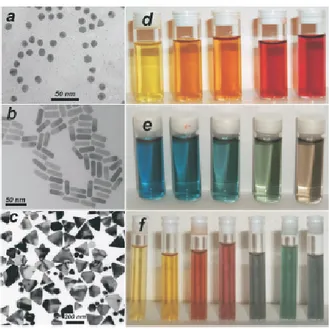
Figure 4: Left: Transmission electron micrographs of (a) Au nanospheres and nanorods (b) and Ag nanoprisms (c) formed using citrate reduction, seeded growth, and DMF reduction, respectively. Right: Photographs of colloidal dispersions of AuAg alloy NPs with increasing Au concentration (d), Au nanorods of increasing aspect ratio (e), and Ag nanoprisms with increasing lateral size (f).?
seeds on which additional metal is grown in solution by means of a mild ascorbic agent (ascorbic acid) allowing to produce elongated nanorods with controlled aspect ratio as a function of the paramaters employed.?, ? Finally the DMF (N,N-dimethylformamide)
reduction method reported by Liz-Marzan et al.? allowed the formation of anisotropic
shapes such as nanoprisms. An overview of the results obtained using these methods is presented in Fig. 4,? which clearly evidence the influence of the size and shape on the
SPR wavelength.
These methods allow tuning easily the shape of the NPs; but do not allow the spa-tial organization of NPs, for example on a substrate surface that is necessary in many applications. An alternative is the production of NPs directly on the surface or “inside” a matrix using, for example, the template method. This method allows synthesizing the desired material within the pores of nanoporous alumina? or polymer? membrane.
Metals can be deposited within the pores of the template membranes by electrochemical reduction of the appropriate metal ions. Electrochemical deposition is accomplished by simply coating one face of the membrane with a metal film and using this metal film as a cathode for electroplating. An example of gold nanorods within the pores of alumina template membrane is shown in Fig. 5, where the dark regions are the gold nanorods.?
9 The main disadvantage of this technique is the template itself, since the size of the pores are limited to ≈50 nm. Thus one can only obtain rods with large diameters (≈40 nm).
Figure 5: Transmission electron micrograph of an alumina template membrane show-ing 70 nm diameter Au nanowires within the pores.?
A more versatile method for producing NPs on a surface with controlled dimensions, size, shape and organization is electron beam lithography.? In this case the substrate
is covered with a conductive resin sensitive to electrons like PMMA. Then an electron beam is projected through a pattern to irradiate the resin. The exposed or non-exposed resin is eliminated through a chemical treatment. The metal is thus removed from the substrate leading to the pattern once the rest of the resin is eliminated. Despite the high degree of control that can be achieved with this method, the high cost, limitations in the minimum size of the NPs (≈20 nm?) and the maximum extension of the sample
(≈ µm2) prevents a wide spread use of this technique.
Angle resolved nanosphere lithography? is also interesting for spatial organization.
In a first step, a nanosphere mask is self-assembled onto a surface followed by metal deposition trough this mask. In general the set mask/substrate is positioned normal to the direction of metal deposition, but an alternative method consists in tilting this set allowing a better control over the size, shape and separation between metal NPs. However, the minimum size of the NPs that can be produced is higher than 70 nm, and the preparation of the mask on a large area is difficult.
As opposed to the methods presented above, physical methods have the great ad-vantage to produce NPs onto or inside a solid matrix on large surfaces (∼ cm2). Ion
10
dispersion is large and post-implantation thermal treatment are typically required.?, ? It
is very difficult to achieve a good control over the morphology of the NPs, moreover, the depth of implantation is limited, which prevents control of the in-depth organization.
Thin film deposition techniques are more versatile methods since they allow pro-ducing not only NPs on a surface, or at a certain depth as ion implantation, but also nanocomposites in which metal NPs and matrix are produced in the same environment. The deposition process is made under controlled atmosphere (vacuum or gas) and materi-als with high purity and complex stochiometry can be produced. Among these methods, the more relevant ones are sputtering,?, ? and pulsed laser deposition.?, ?The sputtering
technique is a physical vapor deposition process in which atoms in a solid target are ejected into the gas phase due to the bombardment of the material by energetic ions. However, this method has limitations drawbacks when producing certain type of mate-rials such as good quality dielectric oxides. In Pulsed Laser Deposition (PLD) a high power pulsed laser beam is focused inside a vacuum chamber on a target of the desired composition. Material is then ejected from the target and deposited as a thin film on a substrate facing the target.? It is a very simple technique from the experimental point
of view, since the target can have almost any geometry, and it does not require polar-izing or cooling the target. PLD can occur in ultra high vacuum or in the presence of a background gas and the composition of the thin film reproduces quite well that of the target. In the configuration of alternate PLD , i.e. using a multiple target holder controlled by computer, it is possible to produce multilayers in a single step process. The characteristics of the deposit can be controlled trough several parameters such as the energy density of the laser, the number of laser pulses on the target, the pressure inside the chamber during the deposit, the configuration of the target-substrate hold-ers, the use of static or rotating substrate holder, etc... Unique features of PLD are its pulsed character and the directionality of the expansion of the plasma generated by laser ablation. While the former favours deposition rates (∼103 nm.s−1),? the latter induces
a non homogenous deposit of the thin film.?
Earlier works performed at the ”Grupo de Procesado por Laser” (GPL) of the In-stituto de ´Optica (IO) have demonstrated the high versatility of this technique for the production of nanocomposite thin films containing metal NPs (Au,? Fe,? Bi,? Ag,? Cu,?
Co?) embedded in a-Al
2O3. Moreover, there are many works from other groups
report-ing the production by PLD of other type of NPs (Au,? Si,? Co,? Pt,? Ge,? CdTe?)
embedded in Al2O3, TiO2 or ZnO. Until now, the works done in the LPG mainly
11 morphological characteristics as well as the optical response of the nanocomposite thin films. In some cases, NPs embedded in a-Al2O3 have also been produced using different
ablation fluences for the metal?, ? or for the a-Al
2O3? matrix. These earlier works have
shown that the size and shape dispersions of NPs produced by PLD is quite reduced for small NPs (< 3 nm), but both increase when the average size increases. Thus, it is imperative to determine the parameters of the PLD or to develop an alternative process which allows reducing the size dispersion and controlling the shape.
Aim of this work
The aim of this work is to determine the experimental conditions that allows “nano-designing” nanocomposite systems containing embedded Ag NPs with small size disper-sion and controlled shape and to relate their optical response to the NPs morphology. When the NPs are elongated (spheroids or nanorods) two distinct SPR bands related to transverse and longitudinal electron oscillations are observed in the optical response, and the latter SPR is very sensitive to the aspect ratio? of NPs. In this respect, it is
challenging to produce elongated NPs with high aspect ratios to tune the longitudinal SPR into the near infra-red. We have chosen Ag as the metal because its SPR is well separated from interband transitions. To reach the objective we have extended the well known alternate deposition conditions for Ag NPs embedded in Al2O3.? The starting
hypothesis is that reducing the in-depth separation between consecutive layers of Ag NPs until they became in contact, the NPs of the consecutive layers might connect and form a stack of NPs, that we will refered to as nanocolumns (NCls).
This work started with the study of the optical properties of Ag NPs as a function of the number of pulses used to ablate the Ag target. This allowed us to relate the morphology of the NPs with their optical properties. At the same time, the conditions to achieve a fine tuning of the a-Al2O3 thickness as a function of the pulse number were
identified. In both cases the geometry of the target-substrate holders was optimized in order to obtain homogenous samples. Once this calibration process was completed we started to produce multilayers of Ag NPs decreasing the thickness of a-Al2O3. These
samples were first characterized by electron microscopy to relate the morphology of the NPs with the parameters used to produce them, and thus, to demonstrate that it is possible to nano-design NCls using a-PLD. In order to demonstrate that we were able to tune the SPR, a systematic study of the optical properties of these samples
12
as a function of angle of incidence and polarization of the light was performed. The experimental results were analyzed within Mie theory and its extension to anisotropic isolated NP (Rayleigh-Gans). The discrepancies between experimental and theoretical results required to introduce a new parameter: the density of NPs, and for this reason we also used an effective medium theory (Maxwell-Garnett). More recently one of our collaborators∗ also made more precise calculations using the open source DDSCAT?
code.
To solve this problem we had used a different type of spectroscopy, i.e. the low fre-quency Raman spectroscopy (LFRS), which gives access to the vibration modes of the NPs. The study of the metal nanostructures, by LFRS, has been initiated by Gersten in 1980, with the first observation of vibration modes in rough copper and silver elec-trodes.? Since then, several works have been performed in this direction and especially
for NPs.?, ?, ?, ?, ?, ?, ? It has been demonstrated that the acoustic vibration of a metal NP
is directly related to the size of the particles and, in particular, Lamb theory? provides
excellent results for estimating NP size. It has also been shown that the vibration of the NPs depends on their geometry,?, ? and as in the case of the SPR, the vibration
modes split into different branches when the NPs are anisotropic. Finally, Bachelier et al. demonstrated that the vibrations of the NPs are directly related to the SPR,? since
the vibration modulates the polarization at the surface of the NPs which affects the os-cillating electrons and thus the SPR. These experiments were performed in Toulouse at the LPST and the interpretation of the results were performed in collaboration with sev-eral researchers around the world†. The results were then compared to the morphology
and the SPR features. The results show that combining extinction spectra and LFRS, which are both accesible and non destructive techniques, one can assess the morphology of NPs.
In parallel to this work, small spherical Co and CoO NPs were produced to study their magnetic properties in collaboration with different research groups‡§. The most
important results of these fruitful collaborations can be found in references.?, ?, ? We used
the knowledge obtained in producing Ag and Co NPs to produce complex nanocompos-ites formed by pairs of Ag and Co NPs layers with well defined separations. Since Ag and Co NPs have specific optical and magnetic properties, respectively, when they are separated, the first aim was to study the effect of this coupling on the magneto-optical
∗Dr A. Arbouet, CEMES, Toulouse, France
†D.B. Murray, University of British Columbia, and L. Saviot, Universit´e Carnot de Bourgogne
‡Prof. Peter Lievens, and his team, Katholieke Universiteit Leuven
13 properties of these samples but, as it happens some times in research, the results ob-tained were not concluding. However, we decided to study these samples using LFRS to further investigate the relationship between SPR and acoustic vibrations. This allowed us detecting the vibration of Co NPs when their distance to Ag NPs decreases. The size parameters were used to calculate∗ the electric field generated by the SPR in the
vicinity of a Ag NPs. This allowed us to demonstrate that the vibrations of Co NPs are excited when the NPs are located in the near field generated by the SPR of the Ag NPs.
Structure of this work
The work is divided in five parts. Part I introduces the work.
Part II focuses on the nano-design. It starts describing the alternate PLD technique: history, principle and experimental setup (Chapter 1). It is followed by the description of the protocol used to nano-design our samples (Chapter 2). Finally, we present the morphology of the samples obtained by this method of production (Chapter 3).
Part III introduces the theoretical optical and vibrational properties of nanocompos-ite thin films containing NPs. We start with the simple case of a bulk metal (Chapter 4) and then, as dimensions are reduced, we present the special properties of metal NPs (Chapter 5).
Part IV presents the optical properties of the thin films produced. The techniques used to acquire the spectra and the special configuration used to study the splitting of the SPRs and vibrations are first shown (Chapter 6). Then we present the results, and analyze them within the theoretical models (Chapter 7). Finally, the SP-SP and SP-vibration coupling are discussed (Chapter 8).
Finally, Part V concludes this work.
Part II
”Nano-Design”
1
Alternate-Pulsed Laser Deposition of Thin
Films
Pulsed laser deposition (PLD) is one of numerous physical thin film deposition
techniques. Other methods include molecular beam epitaxy (MBE) or sputtering depo-sition (RF, Magnetron, ...) for instance. In comparison PLD offers a higher flexibility including a wider choice of target material, laser parameters, target-substrate geometry, and ambient gas and pressure. The PLD technique is based on laser-matter interaction process: a high power pulsed laser beam is focused inside a vacuum chamber to strike a target of a material from which we want to produce a thin film. If the power density is high enough, material is ejected from the target surface, generating a plasma that ex-pands along the direction normal to the target surface. Finally, if a substrate is placed in an appropriate position, a fraction of the ejected material is deposited leading to the growth of a thin film. The experimental conditions: laser fluence, substrate tempera-ture, type and pressure of ambient gas, and geometry of the target-substrate system, determine the characteristics of the deposited films. For example, film growth can take place either in ultra high vacuum or in the presence of a background gas, such as oxygen, which is commonly required when depositing oxides.
18 CHAPTER 1. ALTERNATE-PLD OF THIN FILMS
In this chapter the basic concepts of the PLD technique are introduced. However, a detailed description is out of the scope of the present work and can be found elsewhere.?
1.1
Pulsed Laser Deposition
1.1.1
Introduction
History
The history of laser-assisted film growth started soon after the technical accomplish-ment of the first laser in 1960 by Maiman.? In 1962, Breech and Cross? showed the
ablation of material by laser radiation and studied the laser-ejection and excitation of atoms from solids surfaces. Few years later, in 1965, Smith and Turner demonstrated for the first time the deposition of thin films by ablating materials such as stibnite, ZnTe, PbTe or Ge, with a pulsed ruby laser.? However, the quality of the deposited films was
not as good as that obtained by other techniques which prevented the development of the technique. In the early 1980’s, a few research groups achieved remarkable results on manufacturing thin film using lasers; but the real breakthrough came in 1987 when Di-jkkamp and coworkers?used PLD to produce thin films of the then new high-temperature
superconductor YBa2Cu3O4−δ (YBCO) with a control over the crystalline quality and
the stoichiometry superior to that achieved with any other physical and chemical de-position technique. Since then, PLD has demonstrated its potential to produce high quality crystalline and amorphous films, including ceramic oxides, nitride films, metallic multilayers and various superlattices among other materials. Today PLD is recognized as the best technique for the deposition of oxide thin films. Finally, the development of alternate PLD, which is based on the sequential ablation of different materials, has allowed during the last decade depositing complex structures in thin film configuration such as thin films composed by metallic nanoparticles embedded inside an oxide matrix and multilayers structures.?, ? Nowadays, the development of new laser technologies, i.e.
more competitive lasers having higher repetition rates, energies and new wavelengths, has made PLD a very competitive tool for the production of thin films with well defined complex stoichiometry and complex structures.
1.1. PLD 19 Basic principles
The most important deposition parameters concern the laser (e.g. wavelength, pulse duration, beam profile and pulse energy), the target (e.g. density, absorption coefficient, thermal conductivity, melting temperature, target morphology), the substrate (e.g. ma-terial, crystallinity, temperature), the deposition geometry (substrate placed in or out the expanding plasma), and the gas background (e.g. type of gas and its pressure).?
The appropriate choice of them will determine the final characteristics of the deposited material.
Figure 1.1: Ablation and deposition processes
The processes involved in the film growth by PLD are schematically summarized in Fig. 1.1. A pulsed laser beam is focused on a piece of material we want to grow in thin film configuration: the target. Focusing the laser beam results in a high energy density (fluence) on the target surface, inducing an increase of the temperature immediately followed by the melting and then the ejection of the material. This ejected material is partially ionized and highly excited, and behaves as a transient plasma, which explains the light emission. Due to its shape this plasma is also known as “plume”.
Figure 1.2 shows the light emission of a Ag plasma, the Ag target being ablated using an Excimer UV laser at 193 nm. The kinetic energy of ejected species depends on the angle of incidence of the laser, Φ, and their ejection angle, θ with respect to the target normal (Fig. 1.1). The plasma expands primarily along the normal to the target surface. In this configuration, a fraction of the ablated species reaches the substrate leading to the growth of thin films. Different processes, as diffusion, adsorption, or desorption, may take place at the substrate surface depending on the kinetic energy of the species reaching the substrate. In addition, PLD differs from other physical thin-film deposition
20 CHAPTER 1. ALTERNATE-PLD OF THIN FILMS
Figure 1.2: Plasma plume produced by laser ablation of a Silver target.
techniques by a relatively high instantaneous deposition rate (103 nm s−1) and by a
significant fraction of ions reaching the substrate with high kinetic energy. Plasma generation and expansion
When laser radiation is absorbed in the surface region of a condensed-matter tar-get, the electromagnetic energy is immediately converted into electronic excitation in the form of plasmons, unbound electrons and, in the case of insulators, excitons. The response is regulated by the optical and thermal properties of the target. For pulses longer than 20 ps, ablation is mainly thermally driven. The excited electrons transfer their energy to the lattice within a few picoseconds and heating begins within the opti-cal absorption depth of the material 1/α, where α is the optiopti-cal absorption coefficient. Then the ejection of atoms from the bulk material induced by the laser pulse occurs in a non-equilibrium state.
Ablation of metals is somehow different. Since the penetration depth is typically of 10 nm. Thus, all the photonic energy is absorbed into this very thin layer, and is efficiently transfered to the rest of the target due to its high thermal conductivity. Moreover, for ns pulse ablation, the situation is complicated by ionization of the nascent erosion cloud before the laser pulse is over, which has the effect of dissociating species ejected from the surface.
The temperature of the plasma is typically few thousands of kelvin degrees. This plasma is characterized by an extremely high degree of supersaturation (105 J/mole),
1.1. PLD 21 i.e. far away from the thermodynamical equilibrium, a high degree of ionization, and by the presence of species having high kinetic energies. Depending on the laser parameters and the background gases these kinetic energies can range from 10−1 eV to several 102’s
eV.
Characteristics of PLD
One of the advantages of this technique is that the vacuum system is totally indepen-dent from the laser source. This implies that PLD can easily be adapted to different operational modes without any constraints imposed by the use of internally powered evaporation sources. This allows modifying the ablation conditions by modifying the laser parameters. Moreover, in the case of alternate PLD, targets of different materials are moved alternatively into the beam, thus allowing the alternate deposition of different materials leading to the growth of multilayer structures in a single step process, without breaking the vacuum conditions. The stoichiometry of the target is generally preserved in the deposited films. This makes PLD suitable for the deposition of complex oxides with the desired composition, although in many cases an O2 background is required to
achieve the stoichiometry.
1.1.2
Film growth mechanisms
The deposition of the material ejected from the target generally starts by the formation of small clusters on the substrate surface. The formation (nucleation) of these clusters involves several processes, as illustrated in Fig. 1.3. The species arrive to the surface at a rate that depends on their kinetic energies and therefore on the ablation parameters. These atoms can subsequently diffuse over the substrate or cluster surface, encounter other mobile atoms to form moving or fixed clusters, attach to pre-existing film-atom clusters, to be re-evaporated from the substrate or from a cluster, or be detached from a cluster and remain on the substrate surface.
All these processes depend strongly on the presence of a background gas and on the substrate temperature as they affect the kinetics of the plasma species and the mobility of the atoms on the surface, respectively. In this work all the samples have been produced in vacuum and at room temperature. Hence, the kinetic energy and the mobility of the species depend only on the laser parameters and target characteristics.?
22 CHAPTER 1. ALTERNATE-PLD OF THIN FILMS
Figure 1.3: Possible nucleation mechanisms during film growth
The formation of clusters and their growth at the surface, depend mainly on the interaction energies of substrate atoms and atoms reaching the surface; i.e. adatoms. Perfect flat surfaces do not exist in nature, and defects, such as dislocations, vacancies, and edges, act as favorable nucleation sites. Thus, the comparison of the bond strength of the adatom with the substrate to the bond strength of adatom to its surrounding neighbors determines the initial stage of film growth. The relation between the surface energy of the substrate γs and the surface energy of the growing film γf is given by
Young’s equation,
γs = γi+ γfcos φ, (1.1)
where γi is the film-substrate interface energy and φ is the wetting angle of a nucleus
on the substrate. Depending on the relative values of these interaction energies one can distinguish three modes of film growth? (Fig. 1.4):
• a) Frank-van-der-Merwe: Layer-by-Layer growth: In this case the interaction
between substrate atoms and adatoms is higher than between adjacent adatoms
(γs>γf+γi). Energetically, it is more favorable to form layers. Full-monolayer
1.1. PLD 23
Figure 1.4: Possible film growth modes
monolayer thick and essentially lead to complete coalescence before significant clustering occurs.
• b) Volmer-Weber mode: Island growth: Separated three-dimensional islands
are formed on the substrate if the interaction between adatoms is higher than between adatoms and substrate atoms (γs<γf+γi). Island growth occurs mainly
by surface diffusion of adatoms, which leads to condensation of the adatoms in clusters and finally to the growth of islands.
• c) Stranski-Krastanov mode: Layer-plus-Island: This mode is an hybrid form
of the two growth modes described above. The adatoms initially form complete monolayers (Frank-van-der-Merwe), typically 1 to 5 monolayers. Then, since the stress induced by the mismatched lattice spacings increases with the thickness of the deposited layer, adatoms begin to condensate on the surface and nucleate (Volmer-Weber).
Thin film growth mode will thus depend on the pair substrate-film atoms. The amorphous-Al2O3 (a-Al2O3) has been deposited on top of silicon (covered by a native
24 CHAPTER 1. ALTERNATE-PLD OF THIN FILMS
SiO2 layer) or glass substrates, following in both cases the Franck-van-der-Merwe growth
mode. Instead, we take advantage of the Volmer-Weber growth mode of a metal layer on top of an oxide surface to nucleate metal nanoparticles (NPs) on a-Al2O3.?, ? If the
amount of deposited metal is below a certain threshold, the atoms agglomerate forming NPs. Above this threshold, the distance among NPs decreases leading to coalescence of neighbouring NPs. Figure 1.5 is a simplified scheme of the coalescence process that can be defined roughly as “a melting of contiguous NPs into one unique NP”. If we increase the amount of metal above the coalescence threshold, the percolation of all NPs occurs and the process ends with the formation of a continuous layer. Then, the film follows the Franck-van-der-Merwe growth mode.
Figure 1.5: Schematic of the coalescence process.
1.1.3
Relevant features of PLD: Implantation and Re-Sputtering
As mentioned above, a significative fraction of species present in the plasma have high kinetic energies (>100 eV). These species can influence both positively and negatively the growth process, since they can either improve or deteriorate the overall morphology, stoichiometry, and microstructure of the growing film depending on their actual value
1.2. EXPERIMENTAL EQUIPMENT 25 of the kinetic energy.? In the negative side, the impact of high-energy species on the
surface of the growing film can result in bond breaking, subsurface vacancy production and displacement or removal of surface atoms. Implantation and re-sputtering are direct consequence of these phenomena. Indeed, high speed species can be implanted into the substrate, meanwhile others can be ejected from the substrate (Fig. 1.6). Although it is possible to minimize these effects through an adequate control of the experimental parameters, they always exist and must be taken into account for better understanding of the final morphology of the samples.
Substrate
Re-sputtering
Implantation
Figure 1.6: Schematic of the implantation and re-sputtering effects
1.2
Experimental equipment
The PLD set-up used in this work is schematically shown in Fig. 1.7. The main component is a stainless steel vacuum chamber containing target and substrate holders. An ArF excimer laser (Lambda Physics LPX 210i) operating at a wavelength, λArF=
193 nm and having a pulse duration of τArF= 20 ns (FWHM) was computer controlled
via a frequency generator.
The beam enters the vacuum chamber at an angle of incidence of 45◦ with respect
to the target normal. A lens was used to focus the beam on the target surface (focal length = 250 cm). The spot size at the target surface was typically ≈ 0.02 cm2 and
the average fluence used 2.0 ± 0.2 J/cm2. This fluence was kept constant for all the
26 CHAPTER 1. ALTERNATE-PLD OF THIN FILMS
Figure 1.7: PLD experimental setup
energy stability (≈ 10%) and the indetermination on the spot size. In all cases, thin
films were produced in vacuum at room temperature. We used targets of Ag (≥ 99.99%),
Co (≥ 99.99%), and polycrystalline Al2O3 that were pre-ablated prior to the deposition
process to remove any possible surface contamination. The repetition rate was varied from ν = 5 Hz to 20 Hz depending on the target type. Prior to ablation, the chamber was evacuated with a turbo molecular pump down to p1 = 2.0×10⁻⁶ mbar, for Ag and
Al2O3, and p2 = 8.0×10⁻⁷ mbar for Co.
Target and substrate holders were both rotating and their relative geometries, shown in Fig.1.8, were chosen to improve the thickness uniformity of the deposit in a large area (≈ cm2). The substrate was placed at a distance of 35 mm in front of the target and
rotated by an angle θsub of 32◦ with respect to the vertical. As shown in Fig. 1.8 it
is possible to attach up to four targets and four substrates in their respective holders. This design has the advantage that multi-layered systems and several samples can be prepared without opening the vacuum chamber. To avoid any undesired deposition, three unused substrates are placed behind a protective screen. A mobile screen can also
1.2. EXPERIMENTAL EQUIPMENT 27
Figure 1.8: Geometrical configuration of the Target-Substrate holders system
be placed between the target and the remaining substrate to avoid deposition during cleaning of the target surface. The duration of an ablation sequence is defined by the number of laser pulses, laser frequency and the time required for the displacements of the target holders.
In this work, three types of substrates have been used: glass, silicon covered with its native SiO2, and carbon coated mica. Prior to deposition, glass and silicon substrates
were ultrasonically cleaned in a sequence of trichlorethylene, acetone, and ethanol. Glass was used for the optical characterization, whereas silicon and carbon coated mica were used for cross-section and planview imaging by electron microscopy. Samples were si-multaneously produced on the three types of substrates to ensure that the film structure was the same.
Film thickness and growth rate were determined by “in-situ reflectometry” using a He-Ne laser (λHeN e= 632.8 nm) and a lock-in detection technique. This measurement
was performed on a silicon substrate since it leads to a better reflectivity contrast. However, the change of substrate type does not have a significant influence on the growth rate. A more complete description of the reflectivity measurements is given in Chapter 2.
2
Nano-Design with a-PLD
Whatever the technique used, the requirement for material nano-engineering is always the same: control over the size and shape parameters of the nanostructures
with a high precision and reduced size dispersion. This chapter presents the
protocol, developed in the GPL during the last years, used to embed metals NPs in an oxide matrix. This protocol takes advantage of the special features of PLD described in Chapter 1. After a short description of the relevant features for the implementation of the structures presented in this work, detailed guidelines for metal:oxide nanocomposite preparation using PLD are given. These guidelines describes the production of structures containing multilayers of NPs and nanocolumns (NCls) produced in this work.
2.1
Control of deposition rates
In order to achieve the required size control, it is first necessary to relate the deposition rate to the characteristic size parameters of both the a-Al2O3 matrix (layer thickness)
and metal NPs (average diameter).
30 CHAPTER 2. NANO-DESIGN WITH A-PLD
Amorphous-Al
2O
3deposition rate
The deposition rate of a-Al2O3 is determined from “in-situ” reflectivity measurements
obtained during deposition.
Figure 2.1: Simulated and measured reflectivity (632.8 nm) of a growing a-Al2O3 film on silicon as a function of film thickness and ablation time respectively.
Figure 2.1 presents the reflectivity of a growing a-Al2O3 on top of a silicon substrate
simulated using the refractive index of a-Al2O3 deduced from previous measurements?
and considering that the film grows in the Franck van der Merwe mode. The experimen-tal data obtained with a repetition rate of 20 Hz are compared to the simulated data. The observed behavior is typical of dielectric materials on absorbing substrate showing interference maxima and minima as thickness increases. The comparison of Rexp and Rsim allows converting time into thickness (bottom and top horizontal axis of Fig. 2.1,
respectively). In the experimental conditions used in this work, we have determined an average deposition rate of∼0.05 nm/s at 20 Hz, i.e 2.7×10⁻³ nm/pulse and we estimate
2.1. CONTROL OF DEPOSITION RATES 31
0
100
200
300
400
500
0.5
0.6
0.7
Measured reflectivity of Ag
deposited on a thin
film ofAl
2O
3R
el
ec
ti
vi
ty
(
a.
u)
Time (sec)
0
5
10
15
Thickness (nm)
Calculated
reflectivity
(I)
(II)
(III)
Figure 2.2: Simulated and measured reflectivity of a growing Ag film on a-Al2O3 as a function of film thickness and ablation time, respectively.
Metal deposition rate
The growth rate is more difficult to estimate in this case since metal strongly absorbs light. Figure 2.2 presents the simulated reflectivity Rsim of a growing Ag film on
a-Al2O3, for which the metal film is again considered to grow in a layer-by-layer mode.
The simulation does not take into account the formation of metal clusters on the oxide surface. However, the measured data does evidence this fact as it is shown in Fig. 2.2 for a film deposited at a repetition rate of 5 Hz. We observe that the real reflectivity,
Rexp, is higher than the simulated one at the initial stages of growth while for longer
times both the experimental and simulated values become similar. This initial difference is the signature of metal NPs formation. Thus, it is possible to distinguish three regimes in the growth process of metal on an oxide surface.
• Regime I: Volmer Weber regime: Metals atoms form well separated NPs.
• Regime II: Coalescence regime: The amount of metal deposited is large enough
32 CHAPTER 2. NANO-DESIGN WITH A-PLD • Regime III: Franck van der Merwe regime: The percolation threshold has been
reached. The space among the NPs is filled and metal growth follows a layer-by-layer mode.
The separation between regimes I and II is only approximate. We consider it occurs when ∆R = Rexp− Rsim is maximum. Therefore, it is necessary to remain in regime I,
to achieve control over the morphology of the NPs, as coalescence is a random process, which prevents precise control.
Thus, in regimes I and II, the ablation time is first related to the equivalent thickness of metal if the metal layer were continuous. From this value, it is possible to deduce the average diameter knowing the NPs number density on the surface. Figure 2.3 shows schematically the relation between the equivalent thickness of Ag XAg and the final
diameter of the Ag NPs DAg.
Figure 2.3: Schematic view showing the relationship between XAg and DAg
If we consider an area of 1 cm2, the volume occupied by X
Ag nm of silver is:
V (nm)3 = XAg× 1014 (2.1)
This volume is equal to that occupied by the NPs whose number density is ρN P s
expressed in (NPs/cm2). If we consider that all NPs are spheres of diameter D
Ag, the
diameter of one NP is:
DAg (nm) = ! 6 πρN P s × 10 14X Ag "1/3 (2.2) For example, if the number density of Ag NPs is ρN P s=8×10¹²NPs/cm2and XAg=2
nm, the diameter of the NPs should be DAg ≈3.6 nm. However the areal density of NPs
produced by PLD, ρN P s, depends on the NPs size.?, ? Thus, it is necessary to calibrate
2.1. CONTROL OF DEPOSITION RATES 33 to ablate the target. Fortunately, such a calibration is available from the previous experience of the GPL? in the deposition of Ag NPs. Concerning the case of Co, this
calibration has been done during this thesis. Equivalent thickness of a-Al2O3
Figure 2.4: Schematic showing the relationship between XAg and DAg
In the previous cases we have considered that the substrate surface is perfectly flat. Yet, the NPs are embedded, which means that the layer of a-Al2O3, that covers them,
is deposited on a rough surface. The result will be a nanocomposite layer formed by metal NPs embedded in a-Al2O3 matrix. In this case, for the same deposition time of
a-Al2O3, the layer produced will be apparently thicker than the value determined using
the procedure described above.
Then, it is also necessary to introduce the concept of equivalent thickness of a-Al2O3
to tailor correctly the nanostructures. In this case, the value is defined as the thickness of a-Al2O3deposited among the space between NPs, i.e. the thickness of the nanocomposite
layer, plus the thickness of the a-Al2O3 layer deposited further. Figure 2.4 presents a
schematic to understand these considerations.
As a first step, it is necessary to determine the volume of a single NP (VN P), which
is defined as following:
VN P (nm3) =
4
3π× a × b × c (2.3)
where a,b and c are the three semi-axis in the general case of a non-spherical NP given in nm. Then the total volume (VtotalN P s) occupied by the NPs on a surface of 1 cm2 is
34 CHAPTER 2. NANO-DESIGN WITH A-PLD
calculated as:
VtotalN P s (nm3) = VN P × ρN P s (2.4)
where ρN P s is the number density of NPs by surface unit. The total volume of the
parallelepiped is defined as:
Vtotalpara (nm3) = 1× 10¹⁴× X (2.5)
where X is the desired equivalent thickness of a-Al2O3 expressed in nm. The real volume
of a-Al2O3 we need to deposit is the volume of a layer of thickness T , which is given by: Va−Al2O3 (nm
3) = V
totalpara− VtotalN P s = T × 1014 (nm3) (2.6)
Where T is the real thickness of a-Al2O3 required to obtain a nanocomposite layer
having an equivalent thickness X. For example, an equivalent thickness X of 6 nm, that includes Ag NPs with diameter of 3 nm and number density of 8×10¹² NPs/cm2,
corresponds to a thickness T of 4.8 nm.
2.2
Production of complex nanostructures
Basic principle for the production of homogenous“multi-layered” thin films containing metal NPs
2.2. PRODUCTION OF COMPLEX NANOSTRUCTURES 35 The deposition protocol is illustrated in Fig. 2.5 and described below.
1. Deposition of a thin layer of oxide. This layer acts as a buffer layer to smooth any possible defect as long as they are smaller than few nanometers as well as providing the same surface for NPs to nucleate in the multilayer nanostructure. 2. Growth of NPs. If the equivalent thickness, XAg, is lower than 5 nm, metal NPs
will be produced.
3. Deposition of an oxide layer. The spaces among the NPs are first “filled” in leading to a continuous layer and then the desired thickness of oxide is deposited on top of it.
4. Repetition of steps 2 and 3 as many times (N ) as desired. 5. Deposition of a final protective layer of oxide.
According to the structure of the desired thin film, the appropriate parameters (repe-tition rate, laser energy, deposition times) must be selected. The number of targets, the ablation sequence, the parameters in each step, etc... can indeed be modified to obtain more elaborated structures, such as those described in the following sections.
Production of heterogenous “multi-layered” thin films containing metal NPs. Here we describe the extension of the growth protocol to the case of multilayers containing bilayers of Co and Ag NPs. Figure 2.6 shows cross-section schematics of one of these heterogenous “multi-layers” that consists of five “bilayers” of Co and Ag NPs layers embedded in a-Al2O3. The spacing between the bilayers was fixed to 25
nm. Co NPs are spherical and defined by their diameter DCo while Ag NPs are oblate
spheroids defined by their average diameter, DAgand height HAg. The spacing X within
the bilayers can easily be controlled through the deposition of the matrix following the procedure described above.
36 CHAPTER 2. NANO-DESIGN WITH A-PLD
Figure 2.6: Schematic for the production of CoAg multilayers
The deposition protocol can be summarized as: 1. Deposition of a thin a-Al2O3 buffer layer.
2. Growth of Co NPs. The ablation time was chosen to obtain spherical NPs. 3. Deposition of an equivalent thickness X of a-Al2O3.
4. Growth of coalesced Ag NPs to obtain oblate spheroids.
5. Deposition of a second layer of a-Al2O3, having a thickness of (25− X) nm.
6. This protocol is repeated from the step 2 as many times as the number of desired bilayers.
2.2. PRODUCTION OF COMPLEX NANOSTRUCTURES 37
Figure 2.7: Schematic for the production of Ag NCls
Production of Ag NCls
The procedure used to produce NCls is an extension of the approach used to produce Co-Ag NPs bilayers. Figure 2.7 shows cross-section schematics of one film that consists of “multilayers” of Ag NPs embedded in a-Al2O3 with average diameters DAg. In this
case, the spacing X between consecutive layers of Ag NPs was reduced down to values close to DAg.
The first layer of Ag NPs acts as a pattern that defines the number density and the diameter of the final NCls produced, while the matrix acts as a template allowing their oriented growth. The critical step for the production of NCls resides in the very precise control (i.e. within less than 1 nm) of the equivalent thickness of both metal and a-Al2O3.
The sequence can be repeated an arbitrary number of times N to increase the height of the NCls to lead to the situation sketched in Fig. 2.7. The produced NCls are oriented perpendicular to the substrate.
3
Morphology of nanodesigned structures
produced by a-PLD
In Chapter 2 we have presented the protocols used in this work to produce the nanos-tructures. In this chapter we describe the morphology of the resulting Co:Ag:a-Al2O3
and Ag:a-Al2O3 nanocomposite thin films. First, we briefly present the techniques used
for the morphological characterization of our samples. Then we describe the morphology of the samples produced and its dependence on the deposition parameters.
3.1
Electron microscropy
The morphology and structure of the films have been studied by transmission electron microscopy (TEM), high resolution TEM (HREM) and scanning TEM (STEM) in col-laboration with M.I. Ortiz and C. Ballesteros from the University Carlos III of Madrid (Spain) and U. H¨ormann, M.D. Rossell and G. Van Tendeloo from the University of Antwerp (Belgium). These three types of microscopies have been employed to access different types of information such as: NP size and morphology, NP distribution and