HAL Id: hal-00468115
https://hal.archives-ouvertes.fr/hal-00468115
Preprint submitted on 30 Mar 2010HAL is a multi-disciplinary open access
archive for the deposit and dissemination of sci-entific research documents, whether they are pub-lished or not. The documents may come from teaching and research institutions in France or abroad, or from public or private research centers.
L’archive ouverte pluridisciplinaire HAL, est destinée au dépôt et à la diffusion de documents scientifiques de niveau recherche, publiés ou non, émanant des établissements d’enseignement et de recherche français ou étrangers, des laboratoires publics ou privés.
Self-oscillations in field emission nanowire mechanical
resonators: a nanometric DC-AC conversion
Anthony Ayari, Pascal Vincent, Sorin-Mihai Perisanu, May Choueib, Vincent
Gouttenoire, Mikhael Bechelany, D. Cornu, S.T. Purcell
To cite this version:
Anthony Ayari, Pascal Vincent, Sorin-Mihai Perisanu, May Choueib, Vincent Gouttenoire, et al.. Self-oscillations in field emission nanowire mechanical resonators: a nanometric DC-AC conversion. 2010. �hal-00468115�
1
Self-oscillations in field emission nanowire mechanical
resonators: a nanometric DC-AC conversion
Anthony Ayari,†* Pascal Vincent, †* Sorin Perisanu, † May Choueib, † Vincent Gouttenoire, † Mikhael
Bechelany‡, David Cornu, ‡ Stephen T. Purcell †
Université de Lyon, F-69000, France; Univ. Lyon 1, Laboratoire PMCN; CNRS, UMR 5586; F69622
Villeurbanne Cedex, Laboratoire Multimatériaux et Interfaces, Université Lyon 1, CNRS, UMR 5615,
Domaine Scientifique de la Doua, F-69622, Villeurbanne Cedex, France
[email protected] or [email protected]
RECEIVED DATE (to be automatically inserted after your manuscript is accepted if required
according to the journal that you are submitting your paper to)
We report the observation of self-oscillations in a bottom-up nanoelectromechanical system (NEMS)
during field emission driven by a constant applied voltage. An electromechanical model is explored that
explains the phenomenon and that can be directly used to develop integrated devices. In this first study
we have already achieved ~50% DC/AC (direct to alternative current) conversion. Electrical
self-oscillations in NEMS open up a new path for the development of high speed, autonomous
nanoresonators, and signal generators and show that field emission (FE) is a powerful tool for building
new nano-components.
Within the nanodevice world, nanoelectromechanical systems (NEMS) based on resonant components
2 applications such as wireless communications3. Currently the resonators are passive elements in that
they need external AC driving signals to enter into resonance, i.e. they are not used to generate
independent signals. As well the driving signal is so large that it dominates the output signal from the
resonator and makes readout very challenging especially as the device size is reduced to the nanoscale.
Until now, driving a nanocantilever by a DC signal or their use as an independent AC source in NEMS
has not been achieved and this severely limits integration requiring careful architecture to bring an
external AC signal close to the resonator. These limitations are becoming a real bottleneck as
researchers orient towards frequencies reaching the GHz.
Clearly it would be an enormous advantage to generate these signals directly in the device, as for
example in a Gunn diode4 which is an illustration of a generic phenomenon called self-oscillation.
Self-oscillation, as opposed to the ubiquitous driven harmonic oscillator, is the creation of periodic variations
by a constant driving force. This counter-intuitive and intriguing phenomenon appears in a wide range
of fields such as physiology, biology, hydrodynamics and electronics. Respective examples are the heart
beat,5 hair bundling in the inner ear,6 Rayleigh-Benard thermal convection7 and negative differential
resistance electrical devices.4 In this report, we demonstrate the realization of a bottom-up
nanoresonator in the form of a SiC nanowire that generates a tunable AC signal by self-oscillation
during field emission from the nanowire apex. Furthermore we go on to identify the system parameters
that control the oscillations and fully develop a model that simulates well the experiments.
The self-oscillating resonators consisted of cubic mono-crystalline SiC nanowires attached with a
bottom-up method to tungsten tip supports (see ref. 8 for details about the mounting method). These
nanowires are promising candidates for NEMS nanocantilevers due to their low density of defects and
large modulus to density ratio. They were produced by a vapour-solid process allowing fabrication of
large quantities of SiC-based nanowires with diameters φ ~ 20-400 nm.9,10 Nanotubes and nanowires are especially useful for FE due to their high aspect ratio that creates a large field at the tip for a relatively
low applied voltage. Recently the potential of FE nanosources for high frequency applications has been
3 mechanical single-electron transistor,12 and ultra fast pulsed electron sources.13 We chose a simple
single clamped configuration for its versatility, ideal in the exploration of new phenomena in NEMS.
This approach allowed the first observation of driven electromechanical resonances of carbon nanotubes
in a transmission electron microscope14 and the first tunable single clamped nanoresonator15 which were
both later exploited in a double-clamped hybrid (top-down/bottom-up) device.16 FE self oscillations
were studied in two experimental setups: (1) an ultra high vacuum (UHV) chamber equipped with FE
microscopy; (2) a scanning electron microscope (SEM) equipped with a nanometric manipulator.
Measurements were performed on 6 different nanowires. One sample labelled NW1 is shown in the
inset of Figure. 1a.
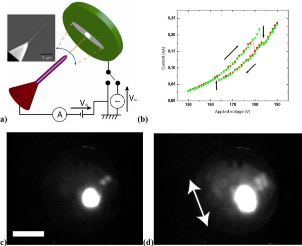
The FE UHV system allows a very stable emission current from the nanowire. Figure 1a is a schema
indicating the tip, DC and AC voltage sources (VDC, VAC) and the phosphor screen on which a FE
pattern is formed by the field emitted electrons that accelerate away from the nanowire apex. The
pattern consists of several bright spots coming from protrusions or nanometric-scale roughness on the
apex which create enhanced local electric fields. Four nanowires (NW1-4) were studied in this setup.
Application of the additional AC voltage allowed us to excite the mechanical resonances in which case
the entire patterns enlarged in one direction and the emitted current varies.15 As well the large static
electric field creates an axial tension Tα VDC2 that tunes the resonance frequency which we will see
below is important for the self-oscillations. The key moment in the experiment occurred when on
increasing VDC with the AC source disconnected, the nanowire image suddenly stretched in one
direction (Figure 1d) exactly as observed under the AC excitation at the resonance frequency (Figure
1a). The oscillation was accompanied by a decrease in the average emission current <IFN > as shown in
Figure 1b. (The picoammeter has a 1 Hz response time and thus only measures time-averaged signals).
Because only a DC voltage was applied we have achieved self-oscillation during FE. The current jumps
and hysteresis occurred reproducibly during voltage scans although the onset might change slightly. It is
4 This FE self-oscillation is the main experimental result and the rest of the article is dedicated to its
comprehension.
The SEM with nanomanipulator allows to modify in situ the geometry of the system and to directly
visualise the position and the motion of the nanowire.17,18 The nanowire was manoeuvred in the vicinity
of a metallic sphere that acted as an anode (Figure 2a). The anode or the tip was connected to either DC
or AC sources as for the FE system. In AC mode the images widened when the frequency was at the
mechanical resonances permitting a measure of the stiffness and quality factor. Application of VDC
could bend the nanowire if it was placed asymmetrically with respect to the centre of the anode as
shown in Figure 2a. Samples NW5 and NW6 have been studied in this setup.
FE was induced from the nanowire apex to the anode for high enough negative VDC applied to the tip.
A DC IFN was then detected on the picoammeter which generally correlated with an increase in the
image intensity, even up to saturation (Figure 2b-c). The SEM uses a secondary electron detector (SED)
for imaging and the increased intensity is due to extra secondary electrons created at the sphere by the
nanowire FE current. VDC used here was ~100V for a φ≈ 100 nm but could be decreased to tens of volts
by approaching the nanowire to the anode or by using a lower diameter nanowire.18 We used a large
diameter sample in this experiment to ease imaging, limit the influence of the SEM electron beam and
lower the resonant frequency, as our nanowires have a fairly constant aspect ratio. On increasing VDC
(and IFN) with the AC generator disconnected, the nanowire image suddenly widened (Figure 2c)
showing that it had again jumped into self-oscillations as in the UHV system. To check that this
vibration was not induced by the SEM beam, we turned off the scanning and moved the beam away
from the nanowire. VDC was then again swept and the SED signal recorded on an oscilloscope. For the
same voltage and current range as before an AC signal was measured (Figure 2d), confirming the
oscillating motion of the nanowire while emitting electrons.
Constructing a viable model depends on identifying and estimating the different elements of the
electromechanical device that may come into play. These include the Young’s modulus E and the
5 apex, the electrical resistivity of the nanowire, the emission current IFN that also transits into the
nanowire, and the nanowire/anode capacitance. The flexibility of the SEM system allows us to measure
most of these parameters directly. It is straightforward to measure E, Q (~4,000), and IFN (pA-100 nA).
The nanowire resistances were measured to be 109-1010 ohms which is typical for this rather large gap
semiconductor. Two methods were used: (1) two point IV measurements directly in the SEM by
touching the end of nanowire to the sphere; (2) analysis of the electron energy spectra of the FE
electrons in the UHV system as previously carried out for carbon nanotubes.19 Further useful
information is gained by comparing the behaviour for the two voltage polarities. With positive polarity
on the nanowire there is no emission for our voltage range because of the large sphere radius and hence
low field enhancement. No nanowire vibrations then occurred showing that the FE current was essential
for self-oscillations. A more subtle aspect which turns out to be critical for the phenomenon is unearthed
when one compares the resonance frequencies for opposite polarities determined by AC excitation as a
function of VDC. The frequency for zero VDC gave E= 500 GPa which is typical for this high quality
nanowire. Figure 2e shows a parabolic behaviour of the resonant frequency due to the electrostatic
tension as observed previously.15,16 For negative VDC below the emission threshold, the resonant
frequencies coincided with those for positive polarity. However above the emission threshold we turned
off the AC signal as well as the electron beam scanning and measured the self-oscillation frequency
with the SED signal. We then observed a clear departure from the positive bias parabola. This is
because now the voltage at the apex which is responsible for the frequency tuning is no longer the same
as VDC due to the voltage drop along these high resistance nanowires. A final important point for the
model, and also for DC/AC conversion, is the variation in IFN during oscillation. From the SED signal in
Figure 2d, we get an AC amplitude of 3V while the average DC voltage is 6 V higher than the one
without field emission. So, we can roughly estimate that the AC component can be as high as fifty
percent of the DC current, which is excellent for a non-optimised geometry.
Previously, torsional self-excitation by mode coupling20 and a laser driven self resonant NEMS where
6 cantilever in an interferometer arrangement. The later approach is inconvenient for an integrated device
and high frequency application compared to a purely electrically driven self resonant NEMS. Thermal
effects, as well as mode coupling, can be ruled out for our samples. With the measured voltage drop
across the nanowire, the current and a thermal conductivity of 1 W m-1 K-1 (rather pessimistic for a SiC
single crystal), we estimate an increase of temperature below 2 degrees. Moreover, at this temperature
the amplitude of the thermal oscillations such as those observed in ref. 22 is lower then 5 nm, much
below the amplitude observed on Figure 1d and Figure 2c. We show next that a model in which only
electromechanical effects are involved explains our experiments.
The motion of the nanowire apex can be described as an oscillator with a variable resonance
frequency due to the electrostatic tension 2
) ( Vx f
T = , submitted to a bending force 2
) ( Vx g
Fb = and with a phenomenological damping factor ω0/Q. We make the approximation that T and Fb are
concentrated at the apex:
x Q m F x bT x eff b & & & 2 0 0 ) (ω + = −ω + (1)
The x axes is represented in Figure 2a, ω0 is the fundamental frequency at VDC =0, meff the effective
mass, f(x) and g(x) two functions that depend on the capacitive environment, V the voltage at the
nanowire apex and b is a constant related to the mass and length of the nanowire.
Using Kirchhoff’s law, the electrical circuit of this NEMS is governed by the following equation:
) ( ) exp( ) ( 2 CV dt d R V V V d V D I NW DC FN − − = − = β β (2)
D and d are constants, β(x) the field enhancement factor (related to the nanowire radius and length and to the distance to the anode), RNW the resistance of the nanowire and C the capacitance between the
grounded anode and the apex. The last term accounts for the cyclic variation of charge.
It is beyond the scope of this work to determine β(x), bf(x), g(x)/meff and C(x), by finite element
simulations. Instead, we performed numerical simulation on simplified equations that can be solved
7 analytical and semi analytical resolution is very useful to prove the absence of numerical instability.
The simplified equations are: + 0 X + 02(X −x0)+ p2V2X =0 Q
X&& ω & ω with X= x0-x and
V C R V V aX I NW DC − = & + + − /(1 2) 0 with exp( )(1 ) 2 0 2 2 0 0 axe V d V D I = − + β
β and xe the equilibrium position
for a given VDC, 2 0 2 2 2 0 0 ω ω + = V p x
xe . The approximate form of the emission current takes into account the
boundary condition and the fact that the nanowire is not perfectly aligned with the anode, i.e. that it
bends upon the application of VDC. The parameters used in the following are for NW6. This gives x0=
20 µm (obtained from Figure 2a), D(β0)2 = 2.2 10-9 AV-2, d/β0 =2276.5 V, RNW=5.109 ohm, p2= 2178576
rad2s-2V-2 (obtained from Figure 2e), ω0=2*π*42150 rad/s, Q=4000, C=10-17 F, a=1011m-2. C and a are
the only unknown parameters. The value of C used here is close to the self capacitance of a sphere of
the same diameter as the nanowire. a is chosen such that aX2 is comparable to one for small amplitude
oscillations.
For the analytical study we injected X=xe+r(t)cos(ωt) (where r(t) is the slowly varying oscillation
amplitude), V=Ue+U0cos(ωt+ϕ)+U1cos(2ωt+ψ) and I= I0/(1+aX2) ≈ I0[A(xe,r)+B(xe,r)cos(ωt)+J(xe,r)
cos(2ωt)] (where
∫
+ + = π ω ω π ω 2 / 0 2 ) cos ( 1 2 a x r t dt A e ,∫
+ = π ω ω π ω2 / 0 2 1 cos dt aX t B and∫
+ = π ω ω π ω2 / 0 2 1 2 cos dt aX t J areFourier coefficients of I for constant r, ω2=ω02+p2V2 and Ue, U0 and U1 are some constants) into our
equations and we checked the stability by looking at the sign of the sin(ωt) component of the mechanical equation. After some algebra, we get :
[
]
− + − − ≈ 2 ( , ) ( , )( ( , )) 2 1 0 0 2 2 0 r x A R I V r x rJ r x B x CI R p r Q dt dr e NW DC e e e NW ω (3)This equation gives the equilibrium positions and their stability.
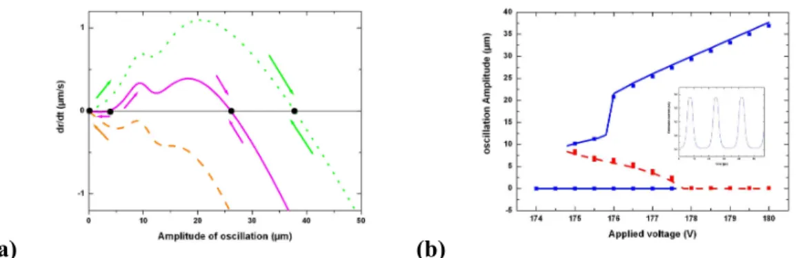
Numerical simulations performed with eqs (1) and (2) and analytical and semi analytical methods
confirmed that they give rise to either immobile or self-oscillating solutions depending on the applied
8 The analytical approaches showed that the variation of C by several orders of magnitude has little
impact on the voltage where self-oscillations appear and the most important ingredients are the x
dependence of β (and of IFN) and the voltage dependence of the resonant frequency, that allows the
energy stored in the capacitance to be re-injected into the mechanical oscillator to cancel the energy
loss. The existence of oscillations is also facilitated by the exponential dependence in IFN and low
damping. Figure 3b shows reasonable qualitative agreement between theory and experiment concerning
the needed DC voltage as well as the AC current amplitude (inset). The immobile solution coexists with
a self-oscillating one over a certain range of voltage and becomes unstable for high enough voltage in
agreement with the hysteresis observed in Figure 1b.
In conclusion we have shown how to create a self oscillating NEMS device. The parameters that
come into play are all elements that can be included in integrated devices, as radio frequency
micromachined devices using FE have already been fabricated.23 We are currently pursuing top-down
and bottom-up methods with the goal of building a functioning device on these principles. We anticipate
that this self-oscillating behaviour will solve one of the major issues of NEMS which is cross talk. The
crucial point here is that a tunable self-oscillating NEMS doesn’t need an external AC source. This is an
important step towards making NEMS active rather than passive devices.
ACKNOWLEDGMENT (Word Style “TD_Acknowledgments”). This work was carried out within
the framework of the Group Nanowires-Nanotubes Lyonnais. The authors acknowledge the support of
the "Centre Technologique des Microstructures de l’Université Lyon 1". M. C. thanks the Lebanese
9
(a) (b)
(c) (d)
Figure 1. (a) Schematic diagram of the UHV system. Inset: SEM image of nanowire NW1 (φ = 30 nm, length (L) 2 µm, resonant frequency in the tens of MHz range) mounted on a tungsten tip. (b) Emission
current as a function of applied voltage for two successive voltage sweeps for NW3 (φ = 200 nm, L=50 µm). The arrows show the direction of sweeping and current jumps. Field emission patterns of the
nanowire NW4 (φ = 30 nm, L= 20 µm) immobile (c) and in self-oscillation (d). The pattern widens in the direction of motion of the nanowire indicated by the white arrow. As the phosphor screen is 3 cm
away from the nanowire and the size of the stretched pattern is about 5 mm (scale bar 1 cm), the
10 (a)
(b) (c)
(d) (e)
Figure 2. (a) Schematic diagram of the SEM system with superimposed, SEM images of NW6 (φ = 400 nm, L= 125 µm) at different static bending, secondary electron emission and electrical connections to
the oscilloscope, AC or DC generators. (b) SEM image of NW5 (φ = 250 nm, L = 270 µm) at rest. (c) The same nanowire in self-oscillation with an amplitude about 1 µm. (d) Signal from the SED for NW6
11 was in AC coupling in order to remove the DC component. (e) Frequency tuning on NW6 ((ο) positive bias, (•) negative bias and (■) emission current).
(a) (b)
Figure 3. (a) Analytical calculation of the derivative of the amplitude dr/dt over time versus amplitude
of oscillation for different applied voltage. The dashed (respectively solid, dotted) line is for VDC = 174
V (respectively 177 V, 180 V). Equilibrium points are shown by filled circles. The arrows indicate the
stability of each point. (b) Stability diagram for different applied voltages. The solid lines are the stable
branches and the dashed line is the unstable branch obtained from analytical calculations. The squares
are obtained from numerical simulations and are in excellent agreement with analytical calculations.
Inset: Emission current as a function of time at equilibrium for VDC = 176 V.
REFERENCES
(1) Knobel, R. G.; Cleland, A. N. Nature 2003, 424, 291.
(2) Ekinci, K.L.; Roukes, M.L. Rev. Sci. Instru. 2005, 76, 061101.
(3) Gammel, P.; Fischer, G.; Bouchaud, J. Bell Labs Tech. J. 2005, 10 (3), 29.
(4) Gunn, J. B. Solid State Commun. 1963, 1, 88.
(5) van der Pol, B.; van der Mark, J. Phil. Mag. 1928, 6, 763.
(6) Crawford, A. C.; Fettiplace, R.; J. Physiol. 1985, 364, 359.
12 (8) De Jonge, N.; Lamy, Y.; Schoots, K.; Oosterkamp, T. H. Nature 2002, 420, 393.
(9) Bechelany, M.; Cornu, D.; Chassagneux, F.; Bernard, S.; Miele, P. J. Opt. Adv. Mater. 2006, 8,
638.
(10) Perisanu S.; Vincent P.; Ayari A.; Choueib M.; Purcell S. T.; Bechelany M.; Cornu D. Appl.
Phys. Lett. 2007, 90, 043113.
(11) Teo, K. B. K.; Minoux, E.; Hudanski L.; Peauger F.; Schnell, J.; Gangloff, L.; Legagneux, P.;
Dieumegard, D.; Amaratunga, G. A. J.; Milne, W. I. Nature 2005, 437, 968.
(12) Scheible, D. V.; Weiss, C.; Kotthaus, J. P.; Blick, R. H. Phys. Rev. Lett. 2004, 93, 186801.
(13) Hommelhoff, P.; Sortais, Y.; Aghajani-Talesh, A.; Kasevich, M. A. Phys. Rev. Lett. 2006, 96,
077401.
(14) Poncharal, P.; Wang, Z. L.; Ugarte, D.; de Heer, W. A. Science 1999, 283, 1513.
(15) Purcell, S. T.; Vincent, P.; Journet, C.; Binh, V. T. Phys. Rev. Lett. 2002, 89, 276103.
(16) Sazonova, V.; Yaish, Y.; Ustünel, H.; Roundy, D.; Arias, T. A.; McEuen, P. L. Nature 2004,
431, 284.
(17) Yu, M-F.; Wagner, G. J.; Ruoff., R. S.; Dyer, M. J. Phys. Rev. B 2002, 66, 073406.
(18) Bonard, J-M.; Dean, K. A.; Coll, B. F.; Klinke C. Phys. Rev. Lett. 2002, 89, 197602.
(19) Purcell, S. T.; Vincent, P.; Journet, C.; Binh, V. T. Phys. Rev. Lett. 2002, 88, 105502.
(20) Kawakatsu, H.; Kawai, S.; Saya D.; Nagashio, M.; Kobayashi, D.; Toshiyoshi, H.; Fujita, H.
Rev. Sci. Instrum. 2002, 73, 2317.
(21) Aubin, K.; Zalalutdinov, M.; Alan, T.; Reichenbach, R.B.; Rand, R.; Zehnder, A.; Parpia,
13 (22) Treacy, M. M. J.; Ebbesen, T. W.; Gibson, J. M. Nature 1996, 381, 678.
(23) Yamashita, K.; Sun, W.; Kakushima, K.; Fujita, H.; Toshiyoshi, H. J. Vac. Sci. Technol. B 2006,
24, 927.