HAL Id: hal-01626127
https://hal.archives-ouvertes.fr/hal-01626127
Submitted on 30 Oct 2017
HAL is a multi-disciplinary open access
archive for the deposit and dissemination of
sci-entific research documents, whether they are
pub-lished or not. The documents may come from
teaching and research institutions in France or
abroad, or from public or private research centers.
L’archive ouverte pluridisciplinaire HAL, est
destinée au dépôt et à la diffusion de documents
scientifiques de niveau recherche, publiés ou non,
émanant des établissements d’enseignement et de
recherche français ou étrangers, des laboratoires
publics ou privés.
Embedded active vision system based on an FPGA
architecture
Pierre Chalimbaud, François Berry
To cite this version:
Pierre Chalimbaud, François Berry. Embedded active vision system based on an FPGA architecture.
EURASIP Journal on Embedded Systems, SpringerOpen, 2006. �hal-01626127�
Embedded active vision system based on an FPGA
architecture
Pierre CHALIMBAUD and Fran¸cois BERRY
LASMEA - UMR 6602 du CNRS
24 avenue des landais
63177 AUBIERE CEDEX
EMail: chalimba, [email protected]
Abstract
In computer vision and more particularly in vision processing, the impressive evolution of algorithms and the emergence of new techniques dramatically increase algo-rithm complexity. In this paper, a novel FPGA-based ar-chitecture dedicated to active vision (and more precisely early vision) is proposed. Active vision appears as an al-ternative approach to deal with artificial vision problems. The central idea is to take into account the perceptual aspects of visual tasks, inspired by biological vision sys-tems. For this reason, we propose an original approach based on a System On Programmable Chip implemented in an FPGA connected to a CMOS imager and an inertial set. With such a structure based on reprogrammable de-vices, this system admits a high degree of versatility and allows the implementation of parallel image processing algorithms.
1 Introduction
FPDs and in particular FPGAs have achieved rapid ac-ceptance and growth over the past decade because they can be applied to a very wide range of applications[15]. One of the most interesting applications of FPGAs is the prototyping of designs to be implemented as gate arrays. Another is the emulation of entire large hard-ware systems. Apart from prototyping, an emerging topic for FPGA applications is their use in custom computing machines. This involves using the programmable parts to ”execute” software, rather than compiling the soft-ware for execution on a regular CPU. For the latter, the notion of such Soft-core CPU or hardware overload of the instruction set becomes crucial. Such approaches of-fer a good trade-off between the performance of fixed-functionality hardware and the flexibility of software-programmable substrates. These different aspects are a great advantage in the design of an embedded sensing sys-tem, in particular when there are several data flows. Like ASICs, the main benefit of these systems is their ability to implement specialized circuitry directly in hardware. However, fast prototyping is easier for FPGAs.
Conse-quently, in the design of a versatile embedded system dedicated to image processing, the FPGA solution proves to be the better way.
In computer vision and especially in vision processing, the impressive evolution of algorithms and the emergence of new techniques drastically increase the complexity of al-gorithms. This computational aspect is crucial for the majority of real-time applications and in most cases pro-grammable devices are the best option. For example, FP-GAs have already been used to accelerate real-time point tracking [9], stereo-vision computing [27], color-based ob-ject detection [10], and video and image compression [11]. In this paper, an architecture dedicated to computer vi-sion is proposed. Our approach towards a smart camera consists in performing most of the early vision processing at the sensor level, before transmitting the information to the main processing unit. This behavior is inspired by the human vision system, where eyes are responsible for attention and fixation tasks, sending to the brain only pertinent information about the observed scene. As a matter of fact, the amount of visual data to be transmit-ted and analyzed is strongly reduced and communication bottlenecks can be avoided. The adaptation of percep-tual aspects from biological vision to artificial systems, which is known as active vision and active perception, is briefly explained in section 2 as the principal motiva-tion of this work. Consequently, the main originality of this work is to use the concepts developed in active vi-sion and more generally in bio-inspired computer vivi-sion in order to design suitable hardware. In the third section, the hardware of the smart camera is described. The tech-nological choices are argued according to the objectives given in the previous section. The different modules are fully described and the different data flows are explained. The fourth section presents the core of the FPGA de-sign, in particular the specific modules like the address generation unit or the Fixed Pattern Noise (FPN) cor-rection unit. Finally, we present the results of two image processing algorithms (motion detection and high-speed template tracking implementation).
2 Active vision systems
One of the numerous objectives in artificial vision re-search is to build computer systems that analyze images automatically, determining what the computer ”sees” or ”recognizes” and ”understands” from the environment. In what follows, the problem is to perform the process of interpretation of sensorial data within an environmental model. The first ways of treating the ”vision problem” used passive vision and dynamic vision approaches. Pas-sive vision comprises the classical analysis of images. The approach that David Marr explicitly advocated [20] and to which many others subscribe, it has led to a thriv-ing research field that has been dominant in visual sci-ence in recent years. From David Marr, ”Vision is a
process that produces from images of the external world a description that is useful to the viewer and not clut-tered with irrelevant information”. David Marr proposes
a model of visual processing that begins by identifying the ”zero-crossings” (edges) in the image, uses this edge information to provide a crude segmentation of surfaces called the 2-D sketch, and finally extracts from this sketch the three-dimensional spatial information. That spatial interpretation is expressed in terms of geometrical prim-itives such as generalized cylinders or cones, so that the only data which must be explicitly stored are the x, y, z locations, alpha, beta, gamma orientations, and aspect ratios of each of the cylinders and a symbolic code of the relations between them. In this way the complex scene is reduced to a highly compressed set of meaningful numbers. The problem with this model is that nobody has ever been able to define how such spatial informa-tion can be reliably extracted from the scene. Moreover, the visual world contains far too many ambiguities to be handled successfully. Dynamic vision is a complementary approach which corresponds to the study of visual infor-mation, but in an unbounded sequence of views. This ap-proach introduces time into the image processing, while movement (measured by optical flow) is used in the per-ception process. Some classical approaches using these strategies revolve around recovering structure from mo-tion.
In contrast to these two approaches, [4], [6] and [7] have proposed the active vision approach. Active vision tech-niques are derived from attempts to simulate the human visual system. In human vision, head motion, saccadic eye movement, and the eye’s adaptation to lighting vari-ations are important in the perception process. Active vision therefore aims to simulate the power of this adap-tation. In other words, active vision is an alternative approach to dealing with artificial vision problems. The central idea, also known as the task-driven paradigm, is to take into account the perceptual aspect of visual tasks. Therefore, instead of a full 3D representation of the ob-served scene, the system is supposed to extract only the information useful for solving a given problem, through a
task-driven observation strategy (Figure 1).
Figure 1: Saccadic eye movements and task-driven strat-egy: Examples of eye-scanning records obtained by Yarbus [1]. Observers were given different in-structions while viewing the picture ”They did not expect him” by Ilya Repin. Each of the traces shows a three minute record of eye scanning with the following instructions: a- Free examination, b- Following request to give the ages of the peo-ple, c- Remember the position of the people and objects in the room.
An artificial active vision system uses observer-controlled input sensors. Its main goal must be actively to extract the requested information in order to solve a given task. A wide literature proposes many systems built around the active vision paradigm. The majority of these systems have been driven by the ”robotic” approach and are based on a robotic head. A large survey up to 1996 can be found in [5] and in [26].
Another trend considers algorithmic aspects and focuses on gaze control using foveated sensors with a log-polar mapping. This method can be applied at the sensor level (imager), at the image processing level or both. At the sensor level, some dedicated imagers based on logarithmic-structured space-variant pixel geometry have been implemented. The main advantage of these methods is the ability to cover wide work-spaces with high acuity and a small number of pixels. Several descriptions of the advantages of using space-variant, or logmap, archi-tectures for video sensors have been proposed [3][2][24]. Another logmap device consists of an emulated sensor based on a conventional CCD and an image warp algo-rithm embedded on a microcontroller [8]. More recently, a new trend towards smaller active vision systems com-parable in size to the human head is pushing the limit of motor, gearbox and camera design [19, 23, 25].
However, as mentioned above, most work dedicated to active vision systems is concentrated in the robotic field. In contrast, the main motivation for the work presented here, is to propose a system truly resulting from the
hu-man visual system. Consequently, our approach needs a dedicated architecture for which the FPGA proves to be essential. This architecture is presented and discussed in the next section.
3 Architectural features
The main purpose of our architecture is to allow the im-plementation of early vision processes as in the human or primate visual system. In these systems it is well known that the first neural layers (in the retina) pre-filter the visual data flow in order to select only the conspicuous information. From this pre-filtered information, an at-tentional processing allows focusing on the selected tar-get. In the literature, several computational models of visual attention can be found. The first representative model was proposed by Koch and Ullman in [18] and has been recently revised by Itti [17]. In these models, the purpose of the saliency map is to combine the ”salient” or ”conspicuous” location information from each of the lower feature maps into a global measure to determine how different a given location is from its surroundings. This technique is used to guide selective attention. The design of our active vision system is based on this kind of approach where we assume that the strategy of visual processes can be divided into three successive tasks:
Attention: This is the initializing step of the process. Whole images are grabbed while waiting for the building of the saliency maps. These maps are built in parallel and represent/code conspicuity within the visual field along particular dimensions (e.g. color, orientation, or motion). The result of this step is a set of ROIs (Regions Of Interest). Focusing: This step allows the generation of the geometry of an ROI (rectangular, tilted, foveal, cir-cular, . . . ) and the optimization of the Signal/Noise Ratio: Contrast optimization in an ROI[21], Track-ing of an ROI in motion, . . .
High-level processing: This last step comprises different kinds of tasks such as identification and classification.
The attention stage needs strong parallelization, on the one hand to respect real-time constraints, and on the other hand because of the intrinsic characteristics of the algorithms. As examples, some classical algorithms in an attention task used to build an efficient saliency map are motion detection, Gabor filters, and color segmen-tation. However, the characteristics of particular visual tasks may require dedicated image processing and only an FPGA approach allows such flexibility. For architec-tures such as these, a Stratix EP1S60 from Altera has been chosen. This choice is detailed below. The need for
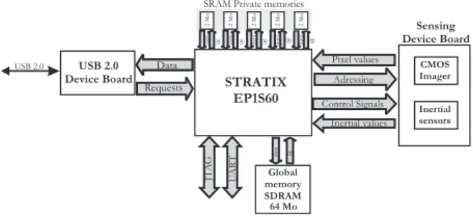
strong parallelization was what led us to connect 5×2MB SRAM synchronous memory blocks. Each 2MB memory has private data and address buses. Consequently, in the FPGA, 5 attention processes (using 2MB each) can ad-dress all the memory at the same time and an SDRAM module socket provides an extension of the memory to 64 MB (Figure 2).
The focusing stage must control the imaging devices in order to address only the ROI and to optimize the ana-log signal conversion. That is the reason why the sensing board has been designed around a CMOS imager and a set of 4 Digital/Analog Converters. A set of inertial sen-sors has been added in order to estimate the movements of the camera and improve the perception (stabilization and depth estimation [22]).
In our approach, the high-level processing has to be per-formed on a host computer rather than on the embedded system. In order to send the data, the smart camera is connected via a high speed communication (USB2.0 or FireWire).
Figure 2: Architecture of the sensor
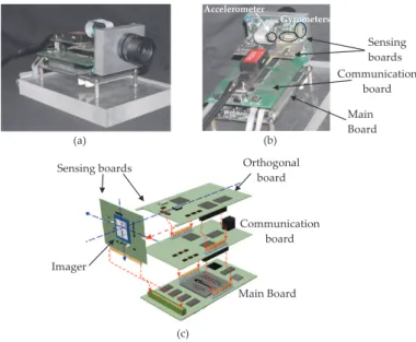
The embedded system is integrated into a modular ar-chitecture consisting of three boards: the sensing board, the processing board and the communication board. An overview of the smart camera is shown in Figure 3 and a structural description presents the stacked structure with 3 boards.
3.1 System On Programmable Chip Features As described in the previous section, the sensor was de-signed around a Stratix EP1S60 manufactured by Altera. This component enables a high density of integration (57120 Logic Elements). It also has three further main advantages which guided our choice.
Firstly, the Stratix is optimized to maximize the perfor-mance benefits of SOPC integration based on a NIOS embedded processor. A NIOS processor is a user-configurable soft core processor, allowing many imple-mentation and optimization options. The NIOS CPU is a pipelined general-purpose RISC microprocessor which supports both 32-bit and 16-bit architectural variants. Both 16 and 32-bit variants use 16-bit instructions. For
Figure 3: a - Front-view of the camera, b- Back-view of the camera, c - Structural description
our sensor, the main advantage of this soft core processor is its extensibility and adaptability. Indeed, users can in-corporate custom logic directly into the NIOS arithmetic logic unit (ALU). Furthermore, thanks to a dedicated bus (Avalon Bus), users can also connect into the SOPC on-chip processor and custom peripherals. They can thus define their own instructions and processor peripherals to optimize the system for a specific application.
Secondly, the Stratix integrates DSP Blocks. These em-bedded DSP Blocks have been optimized to implement several DSP functions with maximum performance and minimum logic resource utilization. Each DSP block of-fers multipliers, adders, subtractors, accumulators and a summation unit, functions that are frequently required in typical DSP algorithms. Each DSP block can also sup-port a variety of multiplier bit sizes (9×9, 18×18, 36×36) and operation modes (multiplication, complex multiplica-tion, multiply-accumulation and multiply-addition) and can offer a DSP throughput of 2.8 GMACS per DSP block. The EP1S160 device has 18 DSP Blocks that can support up to 144 9×9 multipliers. These embed-ded DSP Blocks can also be used to create DSP algo-rithms and complex math routines in high-performance hardware. These can then be accessed as regular soft-ware routines or implemented as custom instructions on the NIOS CPU. For example, a cumbersome algorithm can be implemented in hardware and directly executed in software using a custom instruction. This gives de-signers the flexibility and portability of high-level soft-ware design, while maintaining the performance benefits of parallel hardware operations in FPGAs.
Lastly, the Stratix device incorporates a configurable in-ternal memory called TriMatrix memory. The TriMatrix
memory is composed of three sizes of embedded RAM blocks. The Stratix EP1S60 TriMatrix memory includes 574 M512 blocks (32×18 bits), 292 M4K blocks (128×36 bits), and 6 M-RAM blocks (4K×144 bits). Each of these blocks can be configured to support a wide range of fea-tures and to synthesize a wide variety of RAM (FIFO, double ports). With up to 5 Mbits of fast RAM, the TriMatrix memory structure is therefore appropriate for handling the bottlenecks arising in sensor vision algo-rithms.
3.2 Sensing device
This module consists of a CMOS imager manufactured by Neuricam, two 2D-accelerometers from Analog Devices and three 1D-gyrometers from Murata. The imager al-lows full 2D addressing with a column bus and a row bus. It has a resolution of 640×480 (VGA) and provides a broad dynamic range (120db) due to the logarithmic re-sponse of its pixel structure. Four digital-to-analog con-verters allow modification of the four analog voltages of the imager: analog signal offset, digital conversion range, voltage reference and a pixel precharge voltage. These four converters are used to optimize the conversion range. In effect, the CMOS imager has a logarithmic curve that enables the broad dynamic range (120dB).
Figure 4:Sensing board (a) Front view (b) back view- The white circles show the 4 Digital-Analog Convert-ers. (c) Orthogonal board. (d) Global synoptic of the sensing boards.
The inertial set is composed of two 2D linear accelerome-ters ADXL311 designed by Analog Devices and three gy-rometers EN C03−M designed by Murata. These sensors are soldered onto the imager PCB and aligned with the imager axis. A single 8-input analog-to-digital converter allows conversion of the different axis measurements. It is important to notice that a temperature sensor is included in this board to regulate the inertial sensors’ deviations.
4 Architectural Design
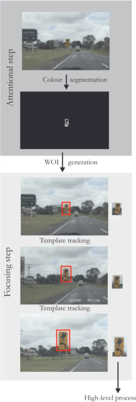
The major difference between biological and artificial vi-sion systems most probably lies in their flexibility. In or-der to develop adaptive capacities, the hardware architec-ture previously described is designed to implement some specific low-level processing dedicated to early vision. This low-level processing attempts to establish an effi-cient interface between sensitive elements and high-level perception systems. As explained in section 3, our strat-egy for efficient visual perception is based on three lay-ers: attention, focusing and high-level processing. This approach adopts a pyramidal method which reduces the amount of data flow. Typically, we can consider a simple system built around an attentional module based only on color segmentation and a focusing module based on tem-plate tracking (Figure 5) In the following, a detailed
de-Figure 5: Example of perception strategy
scription of the FPGA organization is presented. All the ”standard modules” (FPN correction, Addressing mod-ule) are described and designs for focusing and attentional modules are proposed.
4.1 Implementation approach
The implementation of such an approach requires the management, sequentially and concurrently, of the exe-cution of the routines previously described. Indeed, all task-oriented execution (attention, focusing and identifi-cation) is controlled by supplied results and these three layers possibly have to share areas of interest. Moreover, the information bottleneck located in the imager level should be continuously optimized to ensure high perfor-mance. In our hardware architecture, these functions are carried out by what we term a “Sequencer” (6-M0) and are performed on the NIOS soft core processor. This solution has two main advantages. Firstly, we benefit from software flexibility to define the routines’ interac-tions, and secondly, the soft core processor allows an ef-ficient architectural matching with the other parts of the supervision unit.
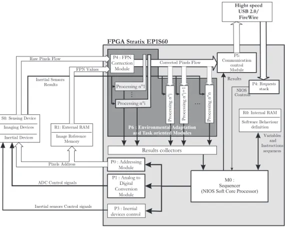
An internal RAM (Figure 6-R0) is used to store the in-struction sequences which define the sequencer behavior according to the task under consideration. The host com-puter which uses our embedded system communicates with it through a standard communication bus (USB 2.0 protocol) and sends requests in order to indicate to the sequencer the relevant behavior to adopt. More precisely, according to the controls (and potentially a set of para-meters) are passed in a dedicated stack, the sequencer chooses pre-established interactions between the modules (Figure 6-P4) which constitute a dedicated processing chain. This architectural module implements the pre-viously described routines of environmental adaptation, attention, focusing and low-level identification (Figure 6-P6). A number of these modules, due to environmen-tal adaptation (Processing No. 1 to i), modify the pixel flow which is going to be used by the attention, focus-ing and identification modules (Processfocus-ing No. j to j+1). The different data flows (corrected windows of interest and inertial measurements) can be used by these mod-ules to perform computing. The set of results that are provided by these processing modules are collected in a buffer. This is how the sequencer selects results to send to the host computer. The sequencer is going to use a part of these results to perform visual feedback on sens-ing devices (Figure 6-S0) ussens-ing dedicated control modules (Figure 6-P0, P1 and P3). We note in Figure 6 the mod-ule P2 which works the external RAM R1. This modmod-ule performs the Fixed Pattern Noise Correction which is ab-solutely essential with the image sensor technology we use (described in section 4.3). Lastly, the dedicated commu-nication module P5 is a multiplexer that synchronizes the corrected pixels flows and the sequencer results flows for sending to the host computer.
Figure 6: Block diagram of architecture adopted
The sequencer constitutes an active interface between the sensing device, processing chain and the host computer. The modular processing chain is synchronized with raw pixel flow control provided by the CMOS imager. Finally, this control allows dynamic control of the global sensor state according to global visual data coherence.
4.2 Addressing module (Figure 6-P0)
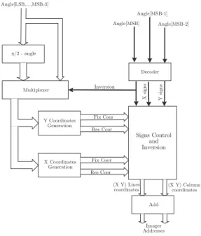
The goal of the address generator device is to com-pute line and column addresses of the current window of interest. The shape of the window is actually rectangular and is set by 5 parameters: position (X,Y), size (H,W) and orientation (α).
The address generation is based on the well-known ”Bre-senham” graphical algorithm [13]. For the computation of the tilted rectangular window addresses, we have im-plemented an architecture based on a recent method for drawing straight lines suitable for raster-scan displays and plotters developed by C. Bond[12].
The approach proposed by Bond is based on signal processing concepts related to resampling, multirate processing and sample rate conversion. The x-coordinates of each pixel can be viewed as a uniform sample set, and the y-coordinates represent another sample set. As-suming the slope of the line is within the first octant, the y-coordinate is generated by resampling the set of
x-coordinates. To control this resampling, the fractional part of the y-coordinate is stored in a control variable as an integer. The algorithm can be summarized by these few lines of code:
• Initialization step Incr=((Y2-Y1)/(X2-X1))*2^n X=X1 Y=Y1 Cvar=1/2*2^n • Loop: repeat{ Cvar+= Incr Y+= Carry X++ } until {X = X2}
(X1, Y 1) and (X2, Y 2) are the coordinates of the segment represented in Figure 7. n is the number of bits which are used to store the fractional part of the y-coordinates. Cvar is the fractional part of the
y-coordinate. Incr is an integer variable used to store slope value. Carry is an overflow indicator for the operation
X Y X1 X2 Y2 Y1 DX DY Octant 1: 000 Octant 2: 001 Octant 3: 010 Octant 4: 011 Octant 5: 100 Octant 6: 101 Octant 7: 110 Octant 8: 111 X Y Qu adran 1:00 Quadra n2 : 01 Qu adran 3 : 10 Quadra n4 : 11
Figure 7: Sampled tilted Line and Octants encoding
Cvar + = Incr;, and (X,Y) are the iterative coordinates
of the line represented in Figure 7.
The extension of the algorithm to other octants is performed by interchanging the roles of x and y, and changing the signs of the coordinates x and y. The internal architecture of the address generator device is illustrated in Figure 8. The range of window tilt is encoded in a natural binary-coded variable named
Angle. The first three MSB bits of this variable define
the octant (Figure 8). The other bits of Angle are used by two functions, based on the Bond algorithm, to generate the fixed-sample variable F ixCoor and the resampled variable ResCoord for each window of interest dimension. According to the quadrant, a decoder defines the sign of the F ixCoor and ResCoord variables. When the line is located in octants 2, 3, 6 or 7, the decoder causes the use of the complementary angle and the inversion of F ixCoor and ResCoord. Finally, the sum of the line coordinates, column coordinates and position vector of the window on the imager give the iterative X and Y address of each pixel. The implementation of this module in the FPGA is characterized by the following parameters:
Total logic elements 150 < 1%
Total memory bits 0 0%
DSP block 9-bit elements 0 0 %
System Clock Frequency 190 MHz
Figure 8: Synoptic diagram of Addressing module
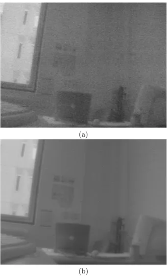
4.3 Fixed Pattern Noise Correction module (P4) Due to the technological limits, a classical CMOS imager (without an embedded CDS correction) provides a raw pixel flow with a high FPN. Indeed, the non-uniformity of the electrical characteristics of each pixel involves an additional stage of correction. In order to even out the electrical response of each pixel, the module called FPN correction module (Figure 6) subtracts the reference values (of the FPN) from the pixel flow. These referent values represent offset differences between each pixel for the same illumination (Figure 9). The set of these values constitutes a reference image. In order to carry out this correction, the sensor integrates a module in order to load it from an external RAM (Figure 6-R1). The implementation of this module in the FPGA is characterized by the following parameters:
Total logic elements 65 < 1%
Total memory bits 85 < 1%
DSP block 9-bit elements 0 0 %
System Clock Frequency 241 MHz
5 Example of attention module implementation: Motion detection
Based on an image difference method (Figure 10), this al-gorithm looks for moving objects in a scene. In the image plan, motion is transduced to temporal and spatial gray-level changes. This module detects temporal changes and defines a rectangular window around the moving object.
(a)
(b)
Figure 9: Images (a) without and (b) with the subtraction of the image reference
In the first step, a difference image is obtained through subtraction of images i and i-1. Then the difference im-age is thresholded, and its vertical projection is calculated (line by line pixel sum in each column). A peak detector is applied to the vertical projection, giving the horizontal position of the moving objects found in the scene. The horizontal projection inside each vertical zone detected previously is then calculated, and a second peak detec-tion is applied to define the vertical posidetec-tion of the moving objects. In this way, it is possible to define the position of several moving objects in the image simultaneously. This information can be used as a parameter for another algorithm, such as a tracker.
6 Example of focusing module: Template tracking
As explained in paragraph 2.2, we assume that an active vision process can be split into three layers: attention, fo-cusing and interpretation. The custom module proposed
Figure 10: Motion detection processus
as an example in this section is a solution to the focus-ing layer. A design dedicated to an efficient template tracking implementation is presented. The main idea of template tracking is to estimate the displacement of a focusing window called W between time t and t + ∂t.
Figure 11: Template tracking module
This module (Figure 11) comprises two parts: a mem-ory to store the reference template denoted I∗ and a
dedicated architecture for the displacement estimation. The architecture adopted is based on a derivation of the Kanade-Lucas-Tomasi algorithm [14]. This algorithm is an iterative method to estimate displacement between two frames (I∗ and I). The proposed method is based
on the calculation of the dissimilarity between two im-ages as follows: ε = Z Z W · I(x +d 2) − I ∗(x −d 2) ¸2 w(x)dx
where x = [x y]T, the displacement d = [d
x dy]T =
∂x
∂t, and the weighting function w(x) is usually set to the
constant 1. To find the displacement d, we set ∂ε
∂d to
I∗ respectively about x − d 2 and x + d2, we obtain: ∂ε ∂d = Z Z W · I(x) − I∗(x) +1 2g T(x)d ¸ g(x)w(x)dx = 0 where g = · ∂ ∂x(I + I∗) ∂ ∂y(I + I∗) ¸ .
Finally, the displacement d can be estimated by solving the equation:
Zd = e
where Z is the following 2x2 matrix
Z =
Z Z
W
g(x)gT(x)w(x)dx
and e is the following 2x1 vector: e = 2
Z Z
W
[I∗(x) − I(x)] g(x)w(x)dx
Due to the Taylor expansion, this algorithm is not exact and needs iterations to find the correct displacement. The estimated displacement at each iteration i is denoted si=
(sxsy)T and is calculated by:
s = 2.Z−1.e where e =¡ PWD.Gx PWD.Gy ¢t and Z = µ P WGx.Gx P WGx.Gy P WGx.Gy P WGy.Gy ¶ . where Gx = ∂(I+I ∗) ∂x , Gy = ∂(I+I∗) ∂y and D = (I∗− I) is
the interframe difference.
The displacement d = (dx dy)T is the result of the
iter-ative process such that d =
i=NX
i=1
si
where N is the maximum number of iterations allowed by the processing. In our case, because of NIOS control, the iterative process is limited to 80 MHz and the pixel flow runs at 8 MHz (corresponding to N = 80
8 = 10 iterations max).
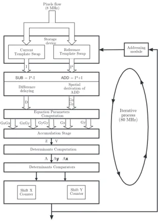
The architecture developed to implement this algorithm is presented in Figure 12. The first module called ”storage device” allows the storage of the reference frame I∗ and
swapping of the current pixel flow between two double-port memories. This module performs the two functions simultaneously in order to ensure the pixel flow rate. The displacement between the reference template I∗ and
cur-rent window I of interest is simultaneously computed dur-ing the storage of the next window of interest.
Figure 12: Implemented architecture
In the first step, the difference (sub) between the two images and the spatial derivatives of their sum (add) are computed and synchronized. The computation of spatial derivatives (Gx and Gy) is based on a set of FIFOs and multiplier-accumulators which apply a (3×3) convolution mask to the data flow. The convolution kernel mask is the Gaussian derivative function.
In the second step, Gx, Gy and Subd are applied to a set
of multipliers in order to compute the coefficients GxGx,
GxGy, GyGy, GxD and GxD. The accumulation of each
allows computation of the elements of Z and e.
The solution is obtained by the evaluation of the following three determinants: Λ =X W Gx.Gx.X W Gy.Gy − (X W Gx.Gy)2 Λx= X W D.Gx.X W Gy.Gy −X W D.Gy.X W Gx.Gy Λy = X W Gx.GxX W D.Gy −X W Gx.Gy.X W D.Gx
According to the signs and the comparison of Λ, Λxand
follows : if kΛxk > kΛk4 then if sign(Λx) ⊕ sign(Λ) then CTx− − else CTx+ + and if kΛyk > kΛk4 then if sign(Λy) ⊕ sign(Λ) then CTy− − else CTy+ +
The updating of the reference template position is car-ried out according to the counter values. This process is iteratively repeated and allows detection of the correct translation vector between the two frames. Lastly, the es-timated translation vector is used to update the position of the window of interest in the CMOS imager in order to track the reference template.
The implementation of this architecture on a Stratix EP1S60 leads to the following parameters:
Total logic elements 4238 7 %
Total memory bits 546 816 10%
DSP block 9-bit elements 94 65 %
System Clock Frequency of the design 140 MHz To illustrate the algorithm, several images and simulation results are presented. This simulation was performed us-ing ModelSim software with the VHDL description of our system.
Figure 13: Results of the template tracking architecture. To evaluate the robustness of the approach, the image is artificially moved with a given displace-ment indicated under each image.
7 Conclusion
The computation of low-level vision tasks in real-time is the first and fundamental step in building an interac-tive vision system. This paper proposes an alternainterac-tive to classical architectures with a highly versatile architec-ture dedicated to early image processing. The proposed embedded system attempts to define a global coordina-tion between sensitive elements, low-level processing and visual tasks.
The approach, based on FPGA Technology and a CMOS imager, reduces the classical bottleneck between sensor and processing. The FPGA component ensures a high interaction rate between the CMOS imager and low-level processing. This interaction is used to select use-ful information earlier in the acquisition chain than for more traditional systems. It then focuses processing re-sources. This capacity is used to control the sensor state according to the visual task and the environment evo-lution. Our implementation of the FPGA and CMOS imager technologies results in high-speed vision, real-environment vision and the efficient design of embedded systems. Among prospective algorithm candidates, we can cite the works performed on dynamically reconfig-urable components such as the ARDOISE1 project [16]. This evolution of FPGA technology seems to be attractive for performing dynamic control of the acquisition chain. Rather than having a control system state, the system it-self can be physically changed and giving a higher level of suitability for many algorithms. We have also developed a DSP board in order to improve the computation capa-bilities of our system. With this device, our embedded system will evolve into a heterogeneous architecture and new research into co-design between the FPGA and the DSP will be necessary.
Moreover, to test the validity of our approach, several visual tasks will be implemented. Our objective is to identify elementary functions in order to define a library of architectural modules. Of course, this library will pro-vide efficient solutions to attention resolution, focusing and identification of sub-tasks according to specific ap-plications. Finally, we plan to work on the development of software tools to facilitate the implementation of com-plex vision tasks
References
[1] A.L. Yarbus. . Eye movements and Vision. Plenum Press, 1967.
[2] Van der Spiegel J. and Kreider G. and Claeys C. and Debusschre I. and Sandini G. and Dario P. and Fan-tini F. and Belluti P. and Soncini G. . A foveated
retina-1ARDOISE: Architecture Reconfigurable Dynamiquement Ori-ent´ee Image et Signal Embarquable
like sensor using CCD technology. Addison-Wesley,
Read-ing, MA. In C. Mead, editor, 1989.
[3] Rojer A. and Schwartz E. L. Design consider-ations for a space-variant visual sensor with complex-logarithmic geometry. In 10th International Conference
on Pattern Recognition, volume 2, Nashville, TN, 1990.
[4] Aloimonos J.Y. and Weiss I. and Bandyopadhyay A. Active vision. In Proceedings of the 1st International
Conference on Computer Vision, pages 35–54, London,
England, June 1987.
[5] Andersen C.S. A Framework for control of a camera
head. PhD thesis, Laboratory of image analysis, Aalborg
Universtity, Denmark, 1996.
[6] Bajcsy R. Active perception. IEEE Proceedings, 76(8):996–1006, August 1988.
[7] Ballard D. Animate vision. Artificial Intelligence, 48(1):1–27, February 1991.
[8] Bederson, B. B. A Miniature Space-Variant Active
Vision System: Cortex-I. PhD thesis, New York
Univer-sity, New York, NY, 1992.
[9] A. Benedetti and P. Perona. Real-time 2-d feature detection on a reconfigurable computer. In CVPR ’98:
Proceedings of the IEEE Computer Society Conference on Computer Vision and Pattern Recognition, page 586,
Washington, DC, USA, 1998. IEEE Computer Society. [10] D. Benitez and J. Cabrera. Reactive computer vi-sion system with reconfigurable architecture. In ICVS
’99: Proceedings of the First International Conference on Computer Vision Systems, pages 348–360, London, UK,
1999.
[11] W. B¨ohm, J. Hammes, B. Draper, M. Chawathe, C. Ross, R. Rinker, and W. Najjar. Mapping a single assignment programming language to reconfigurable sys-tems. J. Supercomput., 21(2):117–130, 2002.
[12] Bond C. A New Line Drawing Algorithm : Based on Sample Rate Conversion. http://www.crbond.com/
papers/newline.pdf, 2002.
[13] Bresenham E. Algorithm for computer control of a digital plotter. IBM Systems Journal, 4(1):25–30, 1965. [14] Tomasi C. and Kanade T. Detection and tracking of point features. Technical report, Carnegie Mellon Uni-versity Technical Report CMU-CS-91-132, April 1991. [15] A. DeHon. The density advantage of configurable computing. Computer, 33(4):41–49, 2000.
[16] Didier Demigny, Nassima Boudouani, Riad Bour-guiba, and Lounis Kessal. Vers une m´ethodologie pour la programmation des architectures `a reconfiguration dy-namique. In In Actes du workshop Ad´equation
Algo-rithmes Architectures En Traitement Du Signal et de L’image, pages 15–20, Janvier 2000.
[17] L. Itti, C. Koch, and E. Niebur. A model of saliency-based visual attention for rapid scene analysis.
IEEE Trans. Pattern Anal. Mach. Intell., 20(11):1254–
1259, 1998.
[18] C. Koch and S. Ullman. Shifts in selective visual attention: Towards the underlying neural circuitry. In
Human Neurobiology, 1985.
[19] Yasuo Kuniyoshi, Noboyuki Kita, Sebastien Rougeaux, and Takashi Suehiro. Active stereo vision sys-tem with foveated wide angle lenses. In ACCV, pages 191–200, 1995.
[20] Marr D. Vision. W H Freeman and Co., San Fran-cisco, 1982.
[21] P. Chalimbaud and F. Berry. Contrast optimiza-tion in a multi-windowing image processing architecture. In IAPR Machine, Vision and Application (MVA’05), Tsukuba, Japon, Mai 2005.
[22] P. Chalimbaud and F. Berry and F. Marmoiton and S. Alizon. Design of a hybrid visuo-inertial smart sensor. In ICRA05 Workshop on Integration of Vision and
Iner-tial Sensors-(InerVis2005), Barcelone, Spain, April 2005.
[23] P.M. Sharkey, D.W. Murray, and J.J. Heuring. On the kinematics of robot heads. IEEE Transactions on
Robotics and Automation, 13(3), 1997.
[24] M. Tistarelli and G. Sandini. On the advantage of polar and log-polar mapping for direct estimation of time-to-impact from optical flow. PAMI, 15(4):401–410, April 1993.
[25] S. Truong, J. Kieffer, and A. Zelinsky. A cable-driven pan-tilt mechanism for active vision. In In Proc.
Australian Conference on Robotics and Automation,
Bris-bane, 1999.
[26] Vieville T. A few steps towards 3d active vision.
Springer Series in Information Sciences, 33, 1997.
[27] J. Woodfill and B. Von Herzen. Real-time stereo vision on the parts reconfigurable computer. In FCCM
’97: Proceedings of the 5th IEEE Symposium on FPGA-Based Custom Computing Machines, page 201,
![Figure 1: Saccadic eye movements and task-driven strat- strat-egy: Examples of eye-scanning records obtained by Yarbus [1]](https://thumb-eu.123doks.com/thumbv2/123doknet/14573869.539959/3.892.493.825.130.342/figure-saccadic-movements-examples-scanning-records-obtained-yarbus.webp)