HAL Id: hal-00750339
https://hal.archives-ouvertes.fr/hal-00750339
Submitted on 10 Nov 2012
HAL is a multi-disciplinary open access
archive for the deposit and dissemination of
sci-entific research documents, whether they are
pub-lished or not. The documents may come from
teaching and research institutions in France or
abroad, or from public or private research centers.
L’archive ouverte pluridisciplinaire HAL, est
destinée au dépôt et à la diffusion de documents
scientifiques de niveau recherche, publiés ou non,
émanant des établissements d’enseignement et de
recherche français ou étrangers, des laboratoires
publics ou privés.
Security enhancements for FPGA-based MPSoCs: a
boot-to-runtime protection flow for an embedded
Linux-based system
Pascal Cotret, Florian Devic, Guy Gogniat, Benoit Badrignans, Lionel Torres
To cite this version:
Pascal Cotret, Florian Devic, Guy Gogniat, Benoit Badrignans, Lionel Torres. Security enhancements
for FPGA-based MPSoCs: a boot-to-runtime protection flow for an embedded Linux-based system.
ReCoSoC: Reconfigurable Communication-centric Systems-on-Chip, Jul 2012, York, United Kingdom.
pp.1-8. �hal-00750339�
Security enhancements for FPGA-based MPSoCs:
a boot-to-runtime protection flow for an embedded
Linux-based system
Pascal Cotret
∗, Florian Devic
†‡, Guy Gogniat
∗, Benoˆıt Badrignans
‡and Lionel Torres
† ∗Laboratoire Lab-STICC, Universit´e de Bretagne-Sud, Lorient†Laboratoire LIRMM, Universit´e Montpellier 2, Montpellier [email protected]
‡Netheos, Montpellier f.devic,[email protected]
Abstract—Nowadays, embedded systems become more and more complex: the hardware/software codesign approach is a method to create such systems in a single chip which can be based on reconfigurable technologies such as FPGAs (Field-Programmable Gate Arrays). In such systems, data exchanges are a key point as they convey critical and confi-dential information and data are transmitted between several hardware modules and software layers. In case of an FPGA development life cycle, OS (Operating System) / data updates as runtime communications can be done through an insecure link: attackers can use this medium to make the system misbehave (malicious injection) or retrieve bitstream-related information (eavesdropping). Recent works propose solutions to securely boot a bitstream and the associated OS while runtime transactions are not protected.
This work proposes a full boot-to-runtime protection flow of an embedded Linux kernel during boot and confidential-ity/integrity protection of the external memory containing the kernel and the main application code/data. This work shows that such a solution with hardware components induces an area occupancy of 10% of a xc6vlx240t Virtex-6 FPGA while having an improved throughput for Linux booting and low-latency security for runtime protection.
I. INTRODUCTION
In embedded systems, MPSoCs (Multi-Processor Systems-on-Chip) are managed by an embedded OS (for instance, uCLinux [13]). This OS manages the tasks distribution over all the processor and hardware IPs connected through a dedicated communication link (which is a security breach usable by the incoming attacker) implemented in the target FPGA chip. Bitstream download can be protected to prevent attacks such as replay. Hardware accelerators are also made for providing a user-defined protection layer during the boot of the OS or the execution of the main application running on an embedded system. Devic et al. [4] proposed a solution to secure the boot of an embedded Linux on a Xilinx ML605 FPGA platform. In such a solution, designers can securely set a Linux-based embedded system; unfortunately, during runtime execution, there is no additional protection mechanism to protect the system against attacks. For instance, an attacker can easily
modify memory contents to make the system misbehave or create denial-of-service. This work presents an extension of the work of Devic et al. [4] to provide the final user a complete protection flow from bitstream download to runtime applications execution.
This paper is organized as follows. Section II describes the threat model taken into account in this work. Section III summarizes works related to bitstream, boot and runtime communication protection. Section V shows how a bus-based MPSoC can be protected with a flexible and reconfigurable solution relying on security-enhanced interfaces. Then, Section VI presents implementation results. Finally, Section VII discusses the security of the solution presented in this work while section VIII concludes and highlights the main perspectives we envision.
II. THREAT MODEL
It is assumed that the FPGA system is exposed to hostile environment where physical but non-invasive attacks, ex-cepted side-channel ones, introduced by Kocher et al. [10], are feasible. Besides that, it is assumed that the target FPGA is trusted. Typically, off-chip bus probing and active probing (injection) are considered in our threat model. We consider all attacks aiming to read, modify or replay code or data directly on the external memory: Linux kernel or application modifications should be detected by security mechanisms. This work focuses on three main attacks:
• Spoofing: an attacker provides a random data value on
the external bus.
• Relocation: an instruction put on the external bus by
the attacker is copied from a different bus address (i.e. the attacker puts the instruction from address #5 while expected value is from address #2).
• Replay: similarly to a relocation attack, the attacker intercepts a valid packet and replays it at an opportune time to make the system misbehave.
While spoofing and relocation affects current memory con-tents, replay can be used to make a downgrade of the
FPGA chip: a former bitstream or an obsolete version of the embedded OS can be uploaded in the FPGA itself: this leads to misbehaviors and denial-of-service which makes the system unusable. Therefore, the only way to access the system is through the external memory and the external bus. A solution would be to encrypt and authenticate the whole external memory. Unfortunately, this solution has a high cost in terms of resources consumption and latency overhead. For many applications, building a flexible solution where only the most critical code and/or data sections to be stored in the external memory are protected with cryptographic services is a good choice. Other parts of the memory can be in plaintext or only authenticated [3]. In this case, attackers still have possibilities to compromise the system by tampering unprotected parts of the external memory. Therefore, the system designer needs additional mechanisms to monitor system activity and detect any abnormal behavior.
III. RELATED WORK A. Bitstream protection
To ensure a complete boot-to-runtime protection, we need to secure the FPGA configuration (the bitstream) against spoofing, relocation and replay attacks. These latter are particularly dangerous because the current approaches pro-posed by FPGA vendors like Xilinx [14] or Microsemi with the ISP (In-System Programming) [15] to ensure bitstream confidentiality and integrity are inefficient against replay. Even if an update may typically be performed to correct a critical security flaw, it is possible to downgrade a system, in order to exploit vulnerabilities present in a previous ver-sion. Nevertheless, academic literature proposes mechanisms against downgrades.
In [6], Drimer describes a solution that ensures up-to-dateness for SRAM FPGAs considering that not only the FPGA chip is trusted but also the whole board. This system with several flash memory slots allows the FPGA to start thanks to a bitstream present in a rescue slot, in case of update failure.
Braeken et al. propose STRES (Secure Techniques for Remote reconfiguration of Embedded Systems) [16] based on STS (Station-to-Station) protocol also requiring processor instantiation. It uses elliptic curve communicating through a TCP/IP connection.
Similarly, Devic et al. propose a protocol [17] that ensures up-to-dateness for volatile FPGAs embedding a non-volatile memory.
B. Boot protection
As described in section II, the kernel is typically stored in an external Flash memory due to the large storage capacity requirement. Generally this memory is off-chip, allowing an attacker to modify the kernel in order to introduce malicious code.
Hash algorithms are classically used to ensure kernel integrity like in [18] where Discretix used such a mechanism
for a secure processor. It is the same principle for Atmel [19] and several others companies.
AEGIS [20] is a well accomplished example of hardware to OS securing but requires having a specific processor with a modified operating system.
More recently, ARM conceived TrustZone [21] to build a boot-to-OS chain of trust. In this scheme the software is protected and monitored thanks to a secure bit added to the bus in the hardware. TrustZone uses RSA-PSS (Rivest, Shamir and Adleman - Probabilistic Signature Scheme) to secure the boot. This asymmetric cryptographic protocol verifies the signature of a second level bootloader but is vulnerable to replay attacks.
In [4], Devic et al. implement on FPGA a boot mechanism that precludes kernel modifications using SHA-256 (Secure Hash Algorithm) hash function preventing from replays attacks and supports updates. Three implementations, (last twos based on hardware acceleration mechanisms), are pro-posed to offer three performance/area overhead trade-offs:
• First based on a soft SHA-256 function. • Second based on a hard SHA-256 crypto core. • And the last one based on a hard SHA-256 crypto core
accessed with DMA (Direct Memory Access) transfers. This work proposed also a flexibility improvement involv-ing asymmetric cryptography (RSA-1024 signature verifica-tion) that allows changing the kernel in external memory without changing the bitstream.
C. Runtime protection
In the literature, several studies have addressed the se-curity of embedded systems [11]. At the communication level, these systems can be protected either by software or hardware mechanisms. Software solutions generally do not require additional hardware but offer low efficiency in terms of latency which can be critical for applications where reactivity is essential to fend off attacks. Regarding NoC (Network-on-Chip)-based architectures, Evain et al. [5] propose a solution where security controls are done in each network interface in a distributed manner. Fiorin [7][8] describes a similar approach with a more detailed implementation. For bus-based communication architecture, one of the most significant work was done by Coburn et al. [1] by an approach similar to Fiorin’s work with a centralized security manager aiming to check read/write access rules without cryptographic features (more latency overhead due to the communication between individual interfaces and the manager). Cotret et al. [2] proposes a latency-efficient alternative for MPSoC based on the ARM AXI bus protocol with flexible security configurations and additional cryptographic features.
This work describes further how this solution can be added to the Linux boot protection flow of Devic et al. [4] to provide a completely secure chain from bitstream download to runtime application execution: such a system should be able to manage updates of OS and protection of runtime transactions in the target multiprocessor system.
IV. ASECURED BOOT-TO-RUNTIME FLOW This work proposes a solution based on some works described in Section III to provide a complete secure flow from bitstream to runtime execution of an embedded Linux OS on a FPGA-based MPSoC architecture. It should prevent an attacker to run its own malicious code introduced in an external memory unit.
A. Flexible boot of an embedded Linux
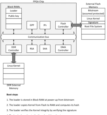
In the existing scheme provided by Xilinx, the bitstream is securely copied from an external Flash to the FPGA and started. In the meantime, block RAMs embedded within the FPGA chip are initialized with a small software called ”bootloader” run by a GPP (General Purpose Processor): the Linux kernel starts once it has been copied by the loader in the DDR external memory (alternatively, the Linux kernel can be transferred from the Flash to the DDR (Double Data Rate) memory using a DMA controller improving the boot time as it can be seen in implementation results). Unfortunately, there is a security breach in such a flow: an attacker can easily update the Flash memory with a malicious kernel because there is no integrity verification of the Flash.
Communication bus
GPP IPs ControllerFlash
DMA Controller SHA RSA DDR Controller Loader Public key Block RAMs Bitstream (assumed protected) Linux Kernel Signature Root File System
Linux Kernel DDR External Memory External Flash Memory Boot steps
1. The loader is stored in Block RAM at power-up from bitstream 2. The loader copies Kernel from Flash to RAM and computes its hash 3. The loader verifies the Kernel integrity by verifying the signature 4. The loader branches to the Kernel and Linux boots
FPGA Chip
Fig. 1. Flexible boot of an embedded Linux
That is the reason why Devic et al. [4] add blocks in the previous flow (Figure 1) to provide a flexible integrity protection layer. In this case, the kernel is copied into the DDR memory. An hash function, implemented in the FPGA (the only trusted area referring to Section II), computes a hash value which is compared by the bootloader with its own kernel hash value: the kernel is started only if values
are equal.
The other implementation, based on an RSA asymmetric cryptographic function allows the final user to change the kernel (in the DDR external memory) without changing the bitstream. This secure boot flow is done in two steps:
• First, the hash function generates the kernel hash value.
• Then, the bootloader (run by the GPP) verifies the signature of the hash value stored in the external Flash memory with the previously generated hash value and its public key.
In Figure 1, the RSA function does not improve the security level of the solution, the only motivation is to add flexibility. At this point, the embedded Linux OS is stored in plaintext in the DDR external memory. This is a major security flaw as an attacker can easily modify DDR contents after boot in order to make the system misbehave: that is why security features must be implemented at the DDR level.
B. Security of the external memory after boot
This work proposes to add confidentiality and integrity features to the DDR external memory, these two features are embedded in a block called CF (Cryptographic Firewall), implementation details are given further in this work. The CF, based on a AES-GCM algorithm, allows the designer to protect the Linux Kernel stored in the DDR external memory with confidentiality and integrity or integrity only, depending on the main application requirements.
Communication bus GPP IPs Flash Controller DMA Controller SHA RSA DDR Controller Loader Public key Block RAMs Bitstream (assumed protected) Linux Kernel Signature Root File System Applications code and data Linux Kernel app1 data2 DDR External Memory External Flash Memory Local F. Local F. Local F. Local F.
Crypto F. Local F. Local F. Local F.
Boot steps
1. Loader is stored in Block RAM at power-up from bitstream
2a. Loader copies Kernel from Flash to RAM (passing through the Crypto Firewall) 2b. Kernel hash is computed thanks to the SHA IP
3. Loader verifies the Kernel integrity by verifying the signature (with the RSA IP) 4. Loader branches to the Kernel and Linux starts
FPGA Chip
Fig. 2. Protection enhancements of the external memory The schematic of Figure 2 shows the CF implemented
in a flow similar to the previous one (Figure 1). In this case, the Linux kernel is not the only entity protected by the Cryptographic Firewall. Any application/data used by a processor in the architecture implemented in the trusted FPGA chip can be protected with flexible security features thanks to the additional logic in the CF (in Figure 2, app1 is protected in confidentiality and integrity while data2 is in plaintext). The decision to protect such and such DDR memory section with full or without security is up to the system designer and depends on the security requirements of the target embedded system. Section V gives details about the structure of runtime security enhancements provided in this work.
V. SECURITY ENHANCEMENTS FOR RUNTIME
PROTECTION
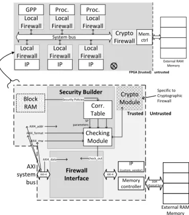
In order to prevent a generic MPSoC system from the threat model detailed in Section II, firewalls are imple-mented within the system. The target system is composed of processors (including a GPP), internal memories, de-dicated IPs embedded within an FPGA and connected to an external memory. Each interface between a peripheral and the communication bus is enhanced with a firewall that aims to monitor communications before they reach the bus and propagate within the system. On the MPSoC shown in Figure 3, there are two categories of firewalls: Local Firewalls and a Cryptographic Firewall (this later adds a layer of cryptographic services towards the external RAM memory). System bus Local Firewall GPP Crypto Firewall External RAM Memory
FPGA (trusted) untrusted
Mem. ctrl
Firewall Interface
Security Builder Crypto
Module Corr. Table Checking Module AXI4_addr AXI4_format AXI4_rnw check_out AXI-4 Block RAM Security Policies AXI system bus IP (custom, vendor) Memory controller External RAM Memory Untrusted Trusted Specific to Cryptographic Firewall AXI-4 DDR physical bus AXI4_data Local Firewall Proc. Local Firewall Proc. Local Firewall IP Local Firewall IP Local Firewall IP SP parameters
Fig. 3. Security-enhanced generic MPSoC architecture
A. Firewall features
Even if the external RAM memory is protected with con-fidentiality and integrity, this work considers that plaintext memory are available and may be used by the attacker to make the system misbehave. Therefore, protecting the external memory with cryptographic services (defined in Section V-D) is not enough: this work proposes to check read/write accesses and data format rules according to designer-defined security policies. These security policies aim to define a security context for a given address space in terms of communications protection (read/write. . . ) and cryptographic services (some address spaces must be ci-phered while others are in plaintext).
These security policies must be stored in entities with adaptivity facilities: updating the security of our system is a key point when an attack is detected. That is the reason why Block RAMs where used: these memory units are easily configurable through a dual-port interface with a dedicated processor. Each firewall (Figure 3) is mainly based on three components:
• Firewall Interface: Communication between the system bus (based on the ARM AXI standard) and the associ-ated IP (custom IP, I/O controller, memory controller): synchronization of handshake signals with datapath-related values. This task is performed by the Firewall Interface.
• Reading Module: Reading security policies defined in on-chip Block RAMs and extracting the parameters. This is done by the Reading Module.
• Firewall Interface: Once parameters were extracted,
their values are compared with some signals of the AXI communication bus. The Checking Module computes a value indicating the validity of bus values from these comparisons and transmits it to the Firewall Interface which blocks or not the datapath within the firewall. In case of attack, read and write access are blocked: if the current request is a write, the firewall simulates the correctness of a write request using handshake signals of the AXI bus standard; in case of read, malicious data is blocked and the firewall sends an error code to the required host processor.
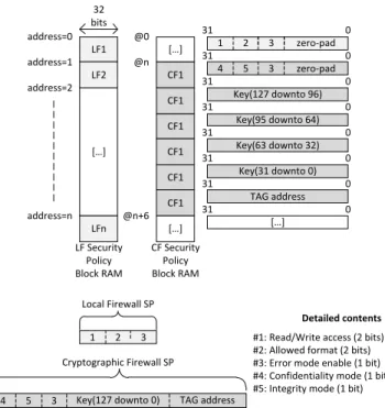
B. Security policies storage
A 16Kb Block RAM (with 32-bit ports) is attached to each firewall (Local and Cryptographic) for SPs (Security Policies) storage. Local Firewall SPs are stored on a single 32-bit block while Cryptographic Firewall SPs are stored on 6 32-bit blocks (LF and CF in Figure 4). Each block is indexed by an address (for instance, address 0) which helps the Reading Module to know where to read the first block of the target Security Policy. In case of reading a Cryptographic Firewall Security Policy, a few logic is added to the Reading Modulein order to read all the SP blocks only knowing the address of the first block.
Figure 4 shows a layout of Block RAMs containing Security Policies for Local and Cryptographic firewalls. As
LF1 TAG address 4 5 Key(127 downto 0) LF Security Policy Block RAM Detailed contents 32 bits address=0 address=1 address=n […] LFn Key(127 downto 96) 31 0 Key(95 downto 64) 31 0 Key(63 downto 32) 31 0 Key(31 downto 0) 31 0 TAG address 31 0 […] 31 0 31 0
#1: Read/Write access (2 bits) #2: Allowed format (2 bits) #4: Confidentiality mode (1 bit) #5: Integrity mode (1 bit) Local Firewall SP Cryptographic Firewall SP CF1 CF1 CF1 CF1 CF1 CF1 […] CF Security Policy Block RAM LF2 address=2 @0 @n @n+6 […] zero-pad 1 2 3 31 0 zero-pad 4 5 1 2 3
#3: Error mode enable (1 bit) 3
3
Fig. 4. Security Policy memory layout for Local and Cryptographic Firewalls
BRAMs data ports are 32-bit wide, a Security Policy for a LF is read in 1 clock cycle instead of 6 cycles for a Cryptographic Firewall SP. Each firewall has its own Block RAM separated from cryptography-related memories (Section V-D).
The structure of fields labeled as #1, #2, #3, #4 and #5 is described in Table I. For confidentiality and authentication,
TABLE I
SECURITYPOLICY STRUCTURE
Values
Field Rule 00 01 10 11
#1 Read all. No No Yes Yes
Write all. No Yes No Yes
#2 Format 4 8 16 32
Values
Field Rule 0 1
#3 Error mode Disabled Enabled Values
Field Rule 0 1
#4 Confidentiality No Yes
#5 Authentication No Yes
related bits allow to correctly connect data ports to the AES-GCM core in order to perform all the needed cryptographic modes (authentication only, plaintext and so on).
C. Security policies update
In case of an attack event, Block RAM contents have to be updated with new SPs through a ”trustworthy processor” in order to keep a safe environment for the target MPSoC. Figure 5 presents the solution implemented in this work.
All the components are connected on an AXI-Lite bus (also known as Reconfiguration bus). An attack monitoring IP has a trusted custom bus connected with each firewall: when an attack event is detected, information is sent back to this IP. The trustworthy processor launches the reconfigu-ration processes on a specific interruption routine from the attack monitoring IP. Depending on the ability of IPs to
Firewall Attack monitoring IP Reconfiguration bus Trustworthy Processor Log timer IP / Processor BRAM controller Data SP BRAM System bus Custom bus Address Firewall IP / Processor BRAM controller SP BRAM Attack flags Attack flags Monitoring path Reconfiguration path recfgEn bit recfgEn bit
Fig. 5. Architecture of the reconfiguration/monitoring area manipulate confidential information, two security flows are established. Critical IPs (for instance, ciphering algorithms implementation) must not reveal any information when an attack event is detected. In that case, critical IPs are isolated from the system (in the error code mode, a fixed designer-defined value is sent instead of the incoming data). For non-critical IPs, an intermediate protection layer is authorized where reading accesses are still allowed but not writing ones. Then, the designer can define a time window where an IP protection mode can be set to a lower security level: in that case, without any attack event detected during a fixed amount of cycles, an IP protection mode can go from ”error code” to the initial configuration.
D. Cryptographic services
This work considers that external memories may not be entirely protected in terms of confidentiality and authenti-cation in order to keep a satisfying area/latency overhead. In this approach, memory sections can be in plaintext, protected with confidentiality and authentication or even authentication only: it allows the system designer to protect only the most critical parts of applications.
The simplest implementation consists in a combination of a basic AES ciphering algorithm and an hash function
(such as MD5 or SHA-2) while muxs and demuxs are used to route signals according to SP parameters related to confidentiality and authentication modes (Cmode and Imode). Unfortunately, this solution has a quite large latency overhead: MD5 computes a hash value in 64 clock cycles while SHA-2 takes 80 cycles to do so.
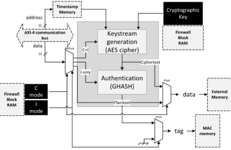
A latency-efficient alternative based on the AES-GCM al-gorithm [3] is proposed in Figure 6. This work uses an AES function to generate a keystream (with timestamp, address inputs and a cryptographic key read from the Block RAM linked with the Cryptographic Firewall) which is XORed with the plaintext to compute the ciphertext. Then, if authentication is required (depending on Cmode and Imode values), datapath goes through the GHASH authentication function [22]. Modes routing (confidentiality/authentication, authentication only, plaintext) is done by one mux and one demux. The use of timestamps and data addresses in the keystream generation within AES-GCM ensures protection against replay and relocation attacks.
In Figure 6, encryption of a 32-bit data block is done in 10
C+I I only C mode I mode Ciphertext address Plaintext tag
data ExternalMemory
MAC memory AXI-4 communication bus Firewall Block RAM Timestamp Memory data mux mux demux 32 32 Cryptographic Key Firewall Block RAM Keystream generation (AES cipher) Authentication (GHASH)
Fig. 6. Cryptographic core based on AES-GCM algorithm clock cycles and authentication in 2 clock cycles: using the AES-GCM algorithm, the Cryptographic Firewall is able to perform low-latency cryptographic services.
E. SMPs extensions
Up until now, embedded systems were supposed to embed only one processor, the General Purpose Processor (GPP). Most of current applications require now, high performance systems: that is the reason why MPSoCs embed several processors; such platforms are also known as SMPs (Sym-metric Multiprocessor platforms). OSs must manage tasks repartition between all the processors of the architecture. From version 2.2, Linux kernel can be configured to manage SMPs: the kernel does all the tasks repartitions by itself according to the availability of all the processors in the target SMPs.
Therefore, for each read/write request, firewalls must be aware of the requesting processor. That is the reason why an ID have to be associated with each transaction between
a processor and an IP. The solution proposed in this work is shown in Figure 7. Here, there is a compromise between
AXI-4 AXI system bus IP (custom, vendor) Memory controller External Memory AXI-4 DDR physical bus Firewall Interface Security Builder Block RAM IDreg Modifications for SMPs compliance
Fig. 7. SMPs extension for firewalls
the architecture complexity (number of wires, buses, connec-tions. . . ) and the latency efficiency of the provided solution. The option we chose is to transmit an ID to be written within a register of the firewall before the transaction itself. In Figure 7, the 4-bit ID (4 bits can code up to 16 IDs) is written in the IDreg register. Then, the transaction (read or write of a data) is processed by the firewall which takes into account the ID in order to block or not the current transaction. Therefore, in terms of latency, the transaction time is doubled because of the register writing before the transaction itself; on the contrary, the architecture of security enhancements is not more complicated as the only change is done in the firewall: an additional register and a few logic (to process the register value as the ID) is enough to make firewalls SMPs-compliant.
VI. IMPLEMENTATION RESULTS
All the following results have been implemented on a Xi-linx ML605 development board including a xc6vlc240t1156-1 Virtex-6 FPGA. This device has around 240,000 logic cells and 15 Mb of Block RAM. First, area and latency overheads of the solution presented in this work are given. Then, some benchmarks are used to study different scenarios overheads for a given case study architecture.
A. Area
First, the idea is to measure the impact of the security enhancements proposed in this work in terms of area. Table II shows the area of a base system composed of a Microblaze processor running at 100 MHz booting a 2.8MB Linux kernel (version 2.631) in a DDR3 external memory connected through an AXI bus. Then, the area of each individual block is given and the overhead is accumulated for each additional block aiming to protect the boot-to-runtime flow (between brackets). As it can be seen in Table II, the area overhead of the boot protection part (SHA, DMA transfer and RSA) is mainly due to the hash function (around 27%). Nevertheless, the whole secured flow applied
TABLE II
AREA OVERHEAD
Slice Slice #
regs LUTs BRAMs
Base system 8,950 9,179 46 + Hard 2,044 2,452 1 SHA-256 (22.83%) (26.71%) (2.17%) + DMA 534 939 4 (28.80%) (36.94%) (10.87%) + RSA-1024 684 989 4 (36.44%) (47.72%) (19.57%) + AES-GCM 2,161 2,689 15 (Crypto Firewall) (60.59%) (77.30%) (52.17%) + Local 123 93 11 Firewall (61.97%) (78.02%) (76.09%)
to a single processor architecture occupies around 10% of a Virtex-6 xc6vlx240t FPGA: some IPs, at least cryptographic ones (SHA, RSA) and DMA, are reusable in the system design.
B. Latency
Latency efficiency is measured through the throughput and the boot time overhead of security enhancement blocks. The throughput of the kernel boot part (first half of Table III) is around 65 MB/s. In case DMA is used to copy the kernel from Flash to DDR, the performance overhead is nil: using the memcpy function, the kernel is booted in 280 ms using the classic Xilinx scheme (the corresponding throughput is 10 MB/s). The security-enhanced boot proposed here is faster with a 12.6 MB/s throughput. Regarding the protection
TABLE III
KERNEL OVERHEADS
# cycles Boot time Throughput Gain overhead
Soft SHA-256 295,860,775 2.959 s 0.95 MB/s ref.
Hard SHA-256 13,650,588 0.137 s 7.29 MB/s x 7.7
+ DMA 4,534,179 0.044 s 66.67 MB/s x 70
TABLE IV
CIPHERING OVERHEADS
# cycles Boot time Throughput overhead RSA 93,042 0.001 s N/A AES-GCM 4,037,018 0.008 s 2.68 MB/s (C+I) AES-GCM 367,002 0.0009 s 23.49 MB/s (I only)
of the external memory, the boot time overhead is acceptable (in both confidentiality/integrity and integrity only modes). From an overall point of view, this AES-GCM core is the main bottleneck of the boot-to-runtime flow (throughput is low compared to the secure boot part), this must be improved by enabling pipelining within the AES-GCM function. C. Benchmark applications
In order to measure the impact of the solution proposed in this work for the runtime protection (i.e. once Linux is
booted), some applications from miBench benchmark suite and a set of custom applications such as FFT (Fast Fourier Transform) and CRC (Cycle Redundancy Check) computa-tions have been considered. We consider the following case study: an architecture with a single Microblaze running an embedded Linux has been securely booted using the flow presented in this work. Benchmark applications are stored in a non-volatile memory and have to be copied in the external memory passing through the Cryptographic Firewall CF. For each application, the boot time (i.e. time to copy the application code in the DDR without security enhancement) serves as a reference while three different scenarios are considered: each application is stored in plaintext (PT), with integrity only (I only) or with confidentiality and integrity (C+I) depending on the requirements of the final use of such an application. For all the scenarios, latency
TABLE V
BENCHMARK OVERHEADS
Application Code size Duration Overheads (ms)
(bytes) (ms) PT C+I I only
miBench basicmath 40,940 0.781 0.131 0.245 0.144 bitcnt1 10,876 0.207 0.035 0.065 0.038 bitcnt2 11,004 0.21 0.035 0.066 0.038 bitcnt3 11,668 0.223 0.037 0.069 0.041 bitcnt4 11,292 0.215 0.036 0.067 0.040 bitstrng 11,068 0.211 0.035 0.066 0.039 dijkstra 23,036 0.439 0.074 0.138 0.081 stringsearch 15,476 0.295 0.049 0.092 0.054 Custom choleski 56,564 1.079 0.181 0.338 0.199 crc 26,492 0.505 0.085 0.159 0.093 dft 41,924 0.8 0.134 0.251 0.147 fft 33,284 0.635 0.106 0.199 0.117 fir 21,908 0.418 0.07 0.131 0.077 lu 40,948 0.781 0.131 0.245 0.144 matrix 29,620 0.565 0.095 0.177 0.104 nbody 29,396 0.561 0.094 0.176 0.103 radix 18,916 0.361 0.06 0.113 0.066 wht 17,316 0.33 0.055 0.103 0.060
overheads are negligible (for instance, between 16% and 31% for the dijkstra application). Thanks to the GHASH hash function embedded in the AES-GCM core, a flexible confidentiality/integrity feature is performed by the Crypto-graphic Firewall while keeping acceptable latency overheads in all modes.
VII. DISCUSSIONS AND SECURITY ANALYSIS Communication architectures considered in this work are based on buses. Such architectures are made for small scale systems (around 16 processors and 16 IPs). If the firewall approach has to be fitted to large-scale embedded systems (NoCs), there are pros and cons to be considered.
Large-scale firewalls have basically the same structure as small-scale firewalls: the main difference is the commu-nication protocol managed by the Firewall Interface; oth-erwise, firewalls behavior is unchanged (it is assumed all the information needed for communication analysis can be
extracted). The main bottleneck is at the architecture level: Local Firewalls do not imply a considerable area overhead. The drawback is due to the number of connections of a firewall each time an IP is instantiated:
• A bus connection for the reconfiguration process.
• Another bus connection for the system bus (dealing with the GPP).
• A custom bus connection (for monitoring purposes). Number of connections increases with the number of fire-walls. At a certain point, custom bus must be managed by an arbiter to decide which firewall has the priority on each other in order to avoid deadlocks and denials of service. In this work small-scale systems are targeted, the proposed protection mechanisms through Local and Cryptographic Firewalls allows the system to be protected against the threat model defined in Section II. With the flexible DDR ciphering approach where some parts of the external me-mory can be ciphered while other are in plaintext, the only security breach should be in these ”unprotected” memory. An attacker can read or write in plaintext memory to create malicious code/data: as soon as malicious contents go through a firewall (Local or Cryptographic), read/write rights, format and address memory map validity are checked. Therefore, the only real breach of the solution presented in this work is an attacker reading plaintext memory sections: it is assumed that such contents were defined by the designer (according to system requirements) as minor information we do not care about if they are disclosed.
VIII. CONCLUSION AND PERSPECTIVES
This paper proposes a solution for a secure boot-to-runtime flow of a MPSoC system running an embedded Linux OS. This solution has several advantages: first, thanks to the RSA core, this system is flexible from a software point of view as the OS kernel can be updated without changing the bitstream. Then, on runtime, a low-latency DDR memory protection is given to protect applications with flexible confidentiality and integrity (address space granularity) providing a good area/latency overhead for em-bedded systems requirements (instead of ciphering the whole external memory). The AES-GCM used for this purpose could also be used for the kernel boot: it would noticeably decrease the area overhead of the solution proposed in this work. As for the Linux kernel, firewalls security policies can be easily updated through a dedicated interface if an attack is detected.
ACKNOWLEDGMENT
The work presented in this paper was realized in the frame of the SecReSoC project number ANR-09-SEGI-013, supported by a grant of the French National Research Agency (ANR).
REFERENCES
[1] J. Coburn, S. Ravi, A. Raghunathan, and S. Chakradhar, “SECA: Security-Enhanced Communication Architecture,” in Proc. 2005 Int. Conference on Compilers, Architectures and Synthesis for Embedded Systems (CASES), Sep. 2005, pp. 78–89.
[2] P. Cotret, J. Crenne, G. Gogniat, and J.-P. Diguet, “Bus-based MPSoC security through communication protection: A latency-efficient alter-native,” in Proc. IEEE 20th Annual Int. IEEE Symposium on Field-Programmable Custom Computing Machines (FCCM), Apr. 2012. [3] J. Crenne, R. Gogniat, Guy anand Vaslin, G. Gogniat, J.-P. Diguet,
R. Tessier, and D. Unnikrishnan, “Configurable memory security in embedded systems,” ACM Transactions on Embedded Computing Systems (TECS) (accepted/to appear), vol. Jan., 2012.
[4] F. Devic, L. Torres, and B. Badrignans, “Securing boot of an em-bedded linux on FPGA,” in Proc. ACM/IEEE 18th Reconfigurable Architectures Workshop (RAW), May 2011, pp. 189–195.
[5] J.-P. Diguet, S. Evain, R. Vaslin, G. Gogniat, and E. Juin, “NOC-centric security of reconfigurable SoC,” in Proc. ACM/IEEE 1st Int. Symposium on Network-on-Chips (NOCS), May 2007, pp. 223–232. [6] S. Drimer and M. G. Kuhn, “A protocol for secure remote updates
of FPGA configurations,” in Proc. ACM/IEEE 5th International Workshop on Reconfigurable Computing: Architectures, Tools and Applications, Mar. 2009, pp. 50–61.
[7] L. Fiorin, G. Palermo, S. Lukovic, and C. Silvano, “A data protection unit for NoC-based architectures,” in Proc. IEEE/ACM 5th IEEE/ACM Int. Conference on Hardware/Software Codesign and System Synthe-sis (CODES+ISSS), Sep. 2007, pp. 167–172.
[8] L. Fiorin, S. Lukovic, and G. Palermo, “Implementation of a re-configurable data protection module for NoC-based MPSoCs,” in Proc. IEEE 18th IEEE Int. Symposium on Parallel and Distributed Processing(IPDPS), Apr. 2008, pp. 1–8.
[9] L. Fiorin, G. Palermo, and C. Silvano, “A monitoring system for NoCs,” in Proc. 3rd Int. Workshop on Network on Chip Architectures (NoCArc), Dec. 2010, pp. 25–30.
[10] P. Kocher, “Timing attacks on implementations of Diffie-Hellman, RSA, DSS, and other systems,” Advances in Cryptology -CRYPTO’96, vol. 1109, pp. 104–113, 1996.
[11] S. Ravi, A. Raghunathan, P. Kocher, and S. Hattangady, “Security in embedded systems: Design challenges,” ACM Transactions on Embedded Computing Systems (TECS), vol. 3, no. 3, pp. 461–491, Aug. 2004.
[12] ARM. (2011) AMBA AXI and ACE protocol specification. [Online]. Available: http://infocenter.arm.com/help/index.jsp
[13] uCLinux. (2012) uCLinux - Embedded Linux/Microcontroller Project. [Online]. Available: http://www.uclinux.org/
[14] (2010, Nov.) Virtex-6 FPGA Configuration, user guide. Xilinx corporation. UG360 (v3.2). [Online]. Available: http://www.xilinx.com/support/documentation/user guides/ug360.pdf [15] (2009, Aug.) In-System Programming (isp) of
Ac-tel low-power flash devices using flashpro3. Microsemi (ex Actel) corporation. Version 1.5. [Online]. Available: http://www.actel.com/documents/LPD ISP HBs.pdf
[16] A. Touhafi, A. Braeken, G. Cornetta, N. Mentens, and K. Steenhaut, “Secure Techniques for Remote configuration of Embedded Systems,” in Handbook of Research on Mobility and Computing: Evolving Technologies and Ubiquitous Impacts, Apr. 2011, pp. 930–951. [17] F. Devic, L. Torres, and B. Badrignans, “Secure protocol
imple-mentation for remote bitstream update preventing replay attacks on FPGA,” in Proc. ACM/IEEE 2010 International Conference on Field Programmable Logic and Applications (FPL’10), Sep. 2011, pp. 179– 182.
[18] Discretix Secure Boot (DxSB). Discretix corporation. [Online]. Available: http://www.discretix.com/secureboot/index.html
[19] (2006, Dec.) Safe and secure bootloader implementation. Atmel corporation. Literature no. 6282. [Online]. Available: http://www.atmel.com/dyn/resources/prod documents/doc6253.pdf [20] G. E. Suh, D. Clarke, B. Gassend, M. van Dijk, and S. Devadas,
“AEGIS: Architecture for tamper-evident and tamper-resistant pro-cessing,” in Proc. 17th annual international conference on Super-computing (ICS’03), Jun. 2003, pp. 160–171.
[21] (2009, Apr.) Building a secure system using
trustzone technology. White paper. [Online]. Avail-able: http://infocenter.arm.com/help/topic/com.arm.doc.prd29-genc-009492c/PRD29-GENC-009492C trustzone security whitepaper.pdf [22] J. Crenne, P. Cotret, G. Gogniat, R. Tessier, J.-P. Diguet, and Tessier, “Efficient key-dependent message authentication in reconfig-urable hardware,” in Proc. IEEE International Conference on Field-Programmable Technology (FPT), Dec. 2011, pp. 1–6.