HAL Id: hal-03034199
https://hal.archives-ouvertes.fr/hal-03034199
Submitted on 1 Dec 2020HAL is a multi-disciplinary open access archive for the deposit and dissemination of sci-entific research documents, whether they are pub-lished or not. The documents may come from teaching and research institutions in France or abroad, or from public or private research centers.
L’archive ouverte pluridisciplinaire HAL, est destinée au dépôt et à la diffusion de documents scientifiques de niveau recherche, publiés ou non, émanant des établissements d’enseignement et de recherche français ou étrangers, des laboratoires publics ou privés.
Engineering block copolymer materials for patterning
ultra-low dimensions
Cian Cummins, Guillaume Pino, Daniele Mantione, Guillaume Fleury
To cite this version:
Cian Cummins, Guillaume Pino, Daniele Mantione, Guillaume Fleury. Engineering block copolymer materials for patterning ultra-low dimensions. Molecular Systems Design & Engineering, RSC, 2020, pp.DOI: 10.1039/D0ME00118J. �10.1039/D0ME00118J�. �hal-03034199�
1
Engineering Block Copolymer Materials for Patterning Ultra-Low Dimensions
Cian Cummins,* Guillaume Pino, Daniele Mantione,Guillaume Fleury*
C. Cummins, Univ. Bordeaux, CNRS, Bordeaux INP, LCPO, UMR 5629, F-33600, Pessac, France
CNRS, Univ. Bordeaux, Centre de Recherche Paul Pascal, UMR 5031, 115 Avenue Schweitzer, 33600 Pessac, France
G. Pino, D. Mantione, G. Fleury, Univ. Bordeaux, CNRS, Bordeaux INP, LCPO, UMR 5629, F-33600, Pessac, France
Keywords: Silicon block copolymers; fluoro block copolymers; nanolithography;
advanced copolymer architectures; sub-10 nm patterning.
2
Abstract
The landscape of block copolymer (BCP) lithographic patterning has evolved significantly from the early days of the first generation BCP material, poly (styrene)-block-poly (methyl methacrylate) (PS-b-PMMA). The low Flory-Huggins interaction parameter (χ) of the workhorse material PS-b-PMMA prevents ultra-low dimensional scaling (< 20 nm), which is the lifeblood of the semiconductor industry. In recent years, this bottleneck has been circumvented through the precise engineering of novel BCPs possessing either high χ and low polymerization degree (N) values or complex macromolecular architectures. We provide a synopsis of recently engineered BCP materials, examining the synthetic routes employed and thin film processing used for nanolithography. Fruitful results emanating from silicon and fluorine containing BCPs are emphasized as they provide a promising platform for sub-10 nm scaling. We subsequently examine routes to continue the relentless scaling for logic technologies with a focus on the potential integration of “advanced” BCP architectures in nanomanufacturing.
1. Introduction
For over 50 years, the world has witnessed the doubling of integrated circuit (IC) transistor density biannually. Colloquially referred to as Moore’s Law (based upon Gordon Moore’s forecast in 1965),1 silicon transistor dimensional scaling has been forbiddingly aggressive - from 10 µm in
1971 to today’s state-of-the-art 14 nm process nodes.2 The miniaturization of IC features is the
backbone of the semiconductor industry and one that serves to provide us with faster, smaller and cheaper electronic devices. Chip manufacturers have principally used optical lithography to reach new milestones. Novel approaches have been integrated over the years to achieve scaling and performance demands to sustain Moore’s Law. For example, the application of multiple patterning,
3
litho-etch-litho-etch, litho-freeze-litho-etch, and novel device architectures exemplify the technological strides achieved.3,4,5 However, the (r)evolution of consumer electronics with
internet-of-things (IoT) demands, in conjugation with the narrowing window of optical lithography capabilities has placed the semiconductor industry at a crossroads. New materials and processes are needed now more than ever before.
Over the past 20 years, a plethora of complementary “top-down” and “bottom-up” patterning methodologies have been under scrutiny to continue Moore’s law. Tight specifications are required for logic and memory devices, e.g. defect density, reduced feature sizes, smaller period sizes (referred to as L0), overlay accuracy, etch contrast, rapid resist processing (< 2 mins), and low
temperature processing windows (< 500°C).6 The specifications need to be in line with
complementary metal oxide semiconductor (CMOS) fabrication and thus leads to a small subset of possible options from top-down and bottom-up methods.7 Truly viable options analogous to
current very large scale integration (VLSI) techniques include directed self-assembly (DSA) of block copolymers (BCPs),8,9 nanoimprint lithography (NIL), and electron beam lithography
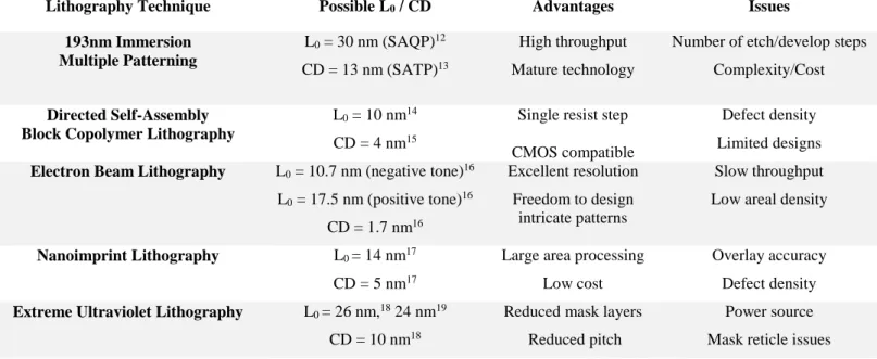
(EBL). Moreover, structures formed must possess a 3σ line edge roughness (LER) and line width roughness (LWR) less than 8% of the critical dimension (CD is used to describe feature sizes from herein). This latter issue becomes ever more problematic as smaller and smaller device dimensions are sought. Table 1 below compares DSA, EBL, and NIL demonstrated L0 and CD versus
state-of-the art techniques currently in chip/memory production: multiple patterning and extreme ultraviolet lithography.10,11
4
Table 1. Comparative table of line-space features demonstrated for next-generation lithography versus current state-of-the-art techniques.
Lithography Technique Possible L0 / CD Advantages Issues
193nm Immersion Multiple Patterning L0 = 30 nm (SAQP)12 CD = 13 nm (SATP)13 High throughput Mature technology
Number of etch/develop steps Complexity/Cost
Directed Self-Assembly Block Copolymer Lithography
L0 = 10 nm14
CD = 4 nm15
Single resist step CMOS compatible
Defect density Limited designs
Electron Beam Lithography L0 = 10.7 nm (negative tone)16
L0 = 17.5 nm (positive tone)16 CD = 1.7 nm16 Excellent resolution Freedom to design intricate patterns Slow throughput Low areal density
Nanoimprint Lithography L0 = 14 nm17
CD = 5 nm17
Large area processing Low cost
Overlay accuracy Defect density
Extreme Ultraviolet Lithography L0 = 26 nm,18 24 nm19
CD = 10 nm18
Reduced mask layers Reduced pitch
Power source Mask reticle issues
Using block copolymer (BCP) thin films as a methodology to create sacrificial masks on a semiconductor surface has garnered immense interest. The DSA-BCP paradigm is strongly considered due to its parallels with traditional CMOS manufacturing due to the related processes employed (substrate preparation, spin coat, bake, and development). Several informative reviews are available on this topic,20,21 and during the preparation of our manuscript, Chen and Xiong
published a comprehensive review on BCPs suitable for sub-10 nm patterning.22 As alluded to
above, it is important to point out to readers that DSA-BCP lithography is viewed as a complementary (rather than disruptive) technology to optical lithography. Several individual group efforts on DSA were published in the 2000’s,23,24,25 however since circa 2009 academic and
industrial consortia initiatives have driven the scaling of BCPs to new frontiers due to BCP material design and process integration.8 In particular, ways to enhance pattern formation and
5
examine BCPs with more vigor.26 BCPs are composed of two distinct chemical polymers in their
simplest configuration, and synthetic advances have been pivotal in the search of BCP materials suitable for nanolithography, as discussed in section 2. A BCPs χ provides us with a measure of the dislike between polymer blocks and is based upon block chemical composition. The volume fraction (f) of the constituent blocks governs the final morphology, while the degree of polymerization (N) mainly dictates the L0. For a lamellar BCP system, strong segregation theory
predicts L0≈ bN2/3χ1/6, where b is the statistical segment length. Reducing a BCP overall N enables
smaller L0. As BCP microphase segregation defined by mean field constraint is only possible once
χN is greater than 10.5,27 high χ BCPs present a route to pattern ultra-low L
0. However, a multitude
of other factors must be studied to facilitate desired BCP microphase segregation. For example, the kinetics of defect annihilation inherent to the formation of lamellar defect-free BCP structures in thin films has been shown to be strongly related to the magnitude of the χN product.28,29
Accordingly, an optimal balance between defect stability and segregation strength (i.e. sharp interface) has to be found in order to design a particular BCP for a targeted L0. Thus, well-balanced
high χ-low N materials and processes that facilitate rapid pattern formation are of significant interest. Surface effects and resulting BCP orientation resulting from respective block surface energies is also critical and must be given particular attention.30
In this review, we firstly survey the recent outstanding reports on silicon and fluorine containing di-BCPs (referred to as Si-BCPs and F-BCPs from here) that have pushed DSA-BCP research forward while also examining some interesting BCP structures derived from PS-b-PMMA. The piece is not exhaustive on high χ materials, rather it is a concise examination of BCP materials of practicality for nanolithography with key criteria being: i) high χ-low N values for sub-16 nm scaling,31 ii) high etch contrast enabling high fidelity pattern transfer,32,33,34 and iii) CMOS
6
compatible processing, e.g. thermal annealing in short periods.35,36 Although we detail solvent
anneal practices due to the flexibility the methodology offers across several BCPs, thermal annealing is the more suitable candidate given the strict solvent and material constraints for high volume manufacturing. The penultimate section deals with “advanced” BCPs where we examine bio-based BCPs, tri-BCPs and precisely tailored macromolecular architectures contribution to the BCP field and we highlight the advances enabled by such designs.
2. High χ-low N BCP synthesis and macromolecular engineering of complex BCP architectures
First, we briefly outline the principal polymerization strategies used for Si- and F-BCPs of late. Several high χ-low N BCPs have been synthesized using anionic polymerization,37 see example in
Scheme 1 below. Anionic polymerization is employed as the quantitative monomer conversion and the absence of a termination reaction allows one precise control of both the degree of polymerization and block volume fraction with good chain-end control.37,38 However, one must
acknowledge that anionic polymerization has various practical limitations. Reaction conditions require highly oxygen-free media without the presence of coupling reactions. As the name suggests, the reaction passes through anionic intermediates. These are extremely reactive and can act like nucleophiles or bases, narrowing the spectrum of reagents and require tedious protecting-deprotecting reactions. Moreover, the stability of the anionic intermediate is highly impacted by the monomer structure, limiting and thus dictating the sequence of monomer addition.
7
Scheme 1. Anionic polymerization of high χ PMOST-b-PTMSS. Images reproduced with permission from Wiley.39
For this reason, alternatives have been sought and controlled radical polymerization (CRP) methods have been shown to form well defined high χ-low N BCPs while being less sensitive to side reactions. Control on volume fraction is achieved by letting the reaction progress until full conversion or stopping it at the optimum moment based on kinetics in order to improve chain-end fidelity. Among CRP methods, the most effective synthesis routes include atom transfer radical polymerization (ATRP),40 reversible addition-fragmentation chain transfer polymerization
(RAFT)41 and nitroxide mediated polymerization (NMP).42 Scheme 2 shows the main equilibria
of ATRP, RAFT, and NMP. Owing to reversibility, reactivity can be controlled with these synthetic methodologies. Despite not involving a radical process, ring opening polymerization (ROP) can also be used, in particular for lactones and cyclic carbonates.43,44,45 ROP uses a cyclic
monomer that is opened using a ω-nucleophile-functionalized macroinitiator (typically a –OH functionalized polymer) in the presence of catalysts.
O sBuLi THF -78°C O O n-1 n THF -78°C Si 1. m 2. MeOH O Si n mH
8
Scheme 2. Main equilibria established during ATRP (top), RAFT (middle), and NMP (bottom) polymerizations.
ATRP uses a leaving atom (typically bromine or chlorine) that is activated by a catalyst (transition metal and ligand), leading to a free radical at the chain-end. In ATRP, an equilibrium between two forms appear: one dormant form bearing the leaving atom, and the other that is propagating, bearing a radical. The main advantage of ATRP is its compatibility with a large variety of monomers possessing an activated double bond, e.g. monomers of styrene, acrylate, methacrylate or acrylonitrile.46 However, some monomers including pyridine-containing monomers can be
inactive because of possible complexation with metal catalysts and require the use of a strongly bonded ligand. We point out that ATRP have been successfully used to synthesize high χ-low N BCPs for nanolithography, however, the use of a metal catalyst is a possible drawback for lithographic applications. This is due to small amounts of metal residing in the final polymer film and therefore in the silicon substrate or more specifically, in the top silicon dioxide layer. This is a critical issue to consider for nanoelectronics where the device layer should be free of metal contamination or defects.
Due to ATRP limitations, RAFT polymerization remains widely used for high χ-low N di-BCPs due to its high versatility of compatible monomers. In RAFT synthesis, the degree of
9
polymerization (DP) is controlled by the ratio [monomer]0/[RAFT agent]0 ; and at low DP the
higher concentration of RAFT agent increases the livingness of the reaction.47 This makes RAFT
an ideal technique for the synthesis of low N BCPs. Methacrylate, styrenic or fluoro-containing monomers have shown very good control in RAFT conditions with dispersity (Đ) values less than 1.1.15 It should however be noted that RAFT agents are only suitable for a limited number of
monomers and thus remain expensive or have to be synthesized in-house. Dithioesters or trithiocarbonates, the most reactive RAFT agents, are highly effective (control on DP, narrow Đ) on more activated monomers such as styrene or methyl methacrylate. On the other hand, RAFT agents presenting a lone pair of electrons adjacent to the thiocarbonyl moiety such as O-alkyl xanthates or dithiocarbamates are less reactive. The latter are more suitable for less activated monomers, where the double bond is adjacent to a saturated carbon like vinyl acetate or N-vinyl pyrrolidone.48 Z and R groups RAFT agent choice (see Scheme 2) is also critical to observe good
control over polymerization while maintaining solvent compatibility.41 For BCP synthesis, a
RAFT agent end-capped macro-initiator may also show poor stability over time or temperature, because of the end chain tend to decompose into smaller sulfur compounds.49 RAFT can also result
in the formation of dead chains if the radical initiator is added in excess quantities. This phenomenon together with the amphiphilic character of high χ BCPs can potentially lead to difficulty during purification for targeting low N BCPs. Finally, for low N BCPs, a RAFT agent can represent up to 15% of the total molecular weight therefore becoming problematic for self-assembly and could potentially necessitate an end-group removal step after BCP synthesis.
NMP was discovered in the early 1980’s and uses a nitroxide as a controlling agent. Nitroxides are stable radicals that can recombine with the radical-bearing chain-end, leading to a dormant species. The recombination is reversible and establishes an equilibrium in the same manner as
10
ATRP and RAFT described above. NMP is inefficient with acrylate or methacrylate monomers, however, more advanced alkoxyamine can be used with MMA or MA monomers.50 For example,
styrenic BCPs and poly(4-vinylpyridine)-b-PMMA (P4VP-b-PMMA) have been synthesized by NMP,51 showing Đ values between 1.1 and 1.2 and conversions up to 99% using 2,2,5-Trimethyl-4-phenyl-3-azahexane-3-nitroxide (universal NMP initiator) and SG1 alkoxyamine. The authors clearly demonstrated the efficiency and versatility of these novel agents. However, like RAFT polymerization, nitroxide compound synthesis can be challenging and is generally limited to commercially available NMP agents or to research groups that are NMP-specialized.52
While the aforementioned BCP synthetic routes are the most widely used for the design of BCPs targeting nanomanufacturing, ring opening metathesis polymerization (ROMP) affords additional versatility in order to create advanced BCP architectures such as bottlebrush BCPs (bBCPs, to be discussed in section 5). bBCPs are very high molecular weight macromolecules consisting of a linear polymer backbone with two different types of polymer side chains connected to it. Three major synthesis paths exists to create such complex architectures: the “grafting from” method consisting in polymerizing monomers from a backbone bearing initiating moieties, the “grafting into” where functional polymers are attached on the backbone and, finally, the “grafting through” method where a macro-monomer bearing the polymer side chain is synthesized first and then polymerized. The last method is the most suitable in making bBCPs with well-defined structural architectures: standardized methodologies rely on the synthesis of norbornene macro-monomers capped with different polymer chains followed by the sequential ROMP using Grubbs catalysts.53,54
11
Finally, progress on the synthesis of molecularly defined oligomers55 via iterative synthetic
procedures involving stepwise monomer coupling and protecting group removal has enabled discrete block co-oligomer production, although the multistep synthetic process may be a roadblock to high volume manufacturing. The most striking examples have been reported by the Meijer and Hawker groups with the synthesis of oligo(dimethylsiloxane)-b-oligo(lactic acid) (ODMS-b-oLA) and oligo(dimethylsiloxane)-b-oligo(methyl methacrylate) (ODMS-b-OMMA) co-oligomers, respectively.56,57 In addition to their inherent low DP benefiting the formation of
mesostructures with small periods, discrete block co-oligomers are also of high theoretical interest. Indeed, the discrete character of their macromolecular structure (Đ → 1) is pertinent to its effect on self-assembly (discussed further in section 6).
In summary, the myriad of BCP polymerization strategies available now constitutes a strong platform for patterning ultra-low dimensions, each with their own distinct advantages and disadvantages. Thus, for high χ-low N BCPs, RAFT and ATRP are highly versatile to produce BCPs favoring highly segregating blocks while still possessing Đ < 1.1. In comparison, NMP can be chosen when the application requires the total absence of metal or sulfur. Overall, choosing a specific strategy is a complex tradeoff for the ultimate designer BCP. For a BCP project targeting aggressive nanomanufacturing, a small L0 is of principal consideration initially, but other criteria
are equally as important and this will be discussed in subsequent sections. For example, BCP solubility with industry compatible solvents like propylene glycol methyl ether acetate,58 similar
block surface energies (γs),59 rapid self-assembly,60,61,62,63 and block compatibility for hard mask
12
3. Silicon containing BCPs
There are two significant reasons for the attention given by researchers to silicon based BCPs for ultra-low L0. Firstly, the silicon moiety is chemically distinct to other fully organic based
polymeric blocks and this enhances the χ considerably. Moreover, silicon containing BCPs provide high etch contrast after plasma etching whereby the silicon block can be converted to silicon dioxide. This renders a robust hard mask for pattern transfer. To date, sub-20 nm L0 have been
realized extensively using poly(styrene)-block-poly(dimethyl siloxane) (PS-b-PDMS) BCPs.66,67,68,69 PS-b-PDMS has been the most studied Si containing BCP for lithography due to its
wide availability. Moreover, commercial PDMS homopolymers are readily available and have been used for in-house synthesis. For example, excellent examples towards sub-20 nm L0 include
poly(2-vinylpyridine)-b-PDMS (P2VP-b-PDMS),70 P4VP-b-PDMS,71 PLA-b-PDMS-b-PLA,72
13
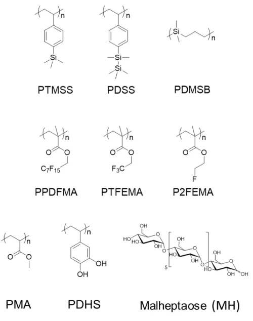
Figure 1. Examples of molecular structures of BCP blocks discussed in this report.
Willson, Ellison and co-workers have demonstrated several high χ-low N silicon based BCPs capable of ultra-low L0.74 Most notably, they developed a top-coat strategy to tune γs at the
polymer/air interface, a considerable advance for lamellar systems.75 Using top-coats they
produced highly uniform thin films of PS-b-poly(trimethylsilylstyrene)-b-PS (PS-b-PTMSS-b-PS) and poly(trimethylsilylstyrene-b-D,L-lactide) (PTMSS-b-PDLLA) with L0 = 29 nm and 19 nm
14
DSA scheme to produce L0 of 19.9 and 17.4 nm respectively.74 The molecular structure of PTMSS
is shown in Figure 1. The systems also showed excellent etch contrast after plasma etching due to the PTMSS blocks conversion to SiOx. Subsequently, PTMSS-b-poly(p-methoxystyrene)
(PTMSS-b-PMOST) and PS-b-poly(pentamethyldisilylstyrene) (PS-b-PDSS) BCPs possessing different compositions have been reported with CD as small as ≈ 5 nm and L0 below 15 nm.39,76,77
More recently, lamellar BCP patterns of poly(5-vinyl-1,3-benzodioxole-b-pentamethyldisilylstyrene) (PVBD-b-PDSS) have been studied to pattern L0 = 10 nm.14 This is one
of the smallest L0 reported to date and showed superb ability to pattern large areas as well as
integration potential in NIL trenches. Through innovative surface engineering and polymer synthesis, Willson and co-workers have created a wide and useful library of Si-BCPs for sub-10 nm lithography. Furthermore, the Si-BCPs are typically thermally annealed in 10 mins or less (see Table 2), a distinct advantage for semiconductor processing. Overall, the aforementioned BCPs provide us with an intriguing insight into a sophisticated methodology to pattern 10 nm lamellar L0 via attention to block chemistry, polymer/substrate and polymer/air interfaces.
15
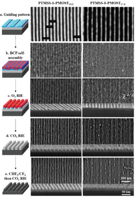
Figure 2. Patterning of two different molecular weight PTMSS-b-PMOST BCPs. Scheme on left illustrates the process flow from BCP alignment to final pattern transfer of features with L0 of 19.9
nm and 17.4 nm respectively. Corresponding top-down SEM images are shown of each step for both periods. Images reproduced with permission from American Chemical Society.74
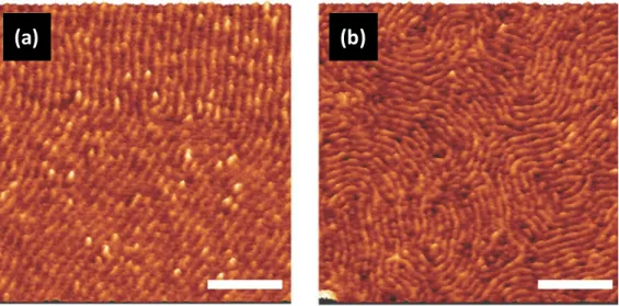
Likewise, Hadziioannou and co-workers have pursued a series of high χ-low N di-BCPs composed of poly(1,1-dimethyl silacyclobutane) (PDMSB) and PMMA or PS blocks. The molecular structure of PDMSB is shown in Figure 1.The engineering of cylinder forming PDMSB-b-PMMA as low as 5.1 kg mol-1 with an L0 = 9.7 nm has been achieved.78 There are various attractive aspects
16
of PDMSB-based systems, including the possibility to produce line-space patterns (see Figure 3) in under 10 minutes through thermal annealing alone. Moreover, high etch contrast is possible together with defined sub-10 nm CD.79,80 The possibility to produce in-situ hardmask materials for
pattern transfer purposes is a very impressive facet of PDMSB based BCPs. PDMSB based ter-BCPs that contain PS, PLA, PMMA or P2VP moieties have also been reported showing exotic BCP arrangements that might be of use for memory devices.81,82,83 Moreover, the PDMSB BCP
work exemplifies the usefulness of cylinder forming BCPs for nanolithography, which were not traditionally favored in the BCP community for line-space applications. On this note, Morris and co-workers have shown the efficacy of cylinder systems for facile pattern transfer with ion inclusion methods.84,85,86
Figure 3. AFM phase images of in-plane PMMA cylinders for PDMSB-b-PMMA films with L0
of (a) 12.7 nm and (b) 9.7 nm. PDMSB-b-PMMA films were cast from toluene onto silicon substrates and thermally annealed for 10 mins. Images reproduced with permission from Wiley.78
(b)
(a)
17
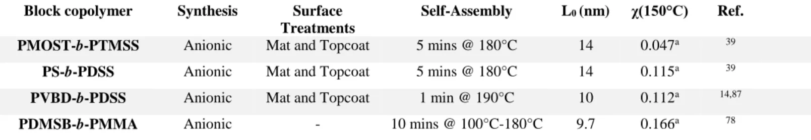
Table 2. Summary of silicon containing BCPs and corresponding synthesis, L0, and χ. aEstimated
using a reference volume of 118 Å3.
Block copolymer Synthesis Surface Treatments
Self-Assembly L0 (nm) χ(150°C) Ref. PMOST-b-PTMSS Anionic Mat and Topcoat 5 mins @ 180°C 14 0.047a 39
PS-b-PDSS Anionic Mat and Topcoat 5 mins @ 180°C 14 0.115a 39 PVBD-b-PDSS Anionic Mat and Topcoat 1 min @ 190°C 10 0.112a 14,87 PDMSB-b-PMMA Anionic - 10 mins @ 100°C-180°C 9.7 0.166a 78
4. Fluorine containing BCPs
The emergence of high χ-low N di-BCPs composed of fluorine moieties is also very evident from recent literature. The chemical immiscibility of fluorine blocks with respect to other organic blocks is the primary characteristic of importance. Further, fluorine blocks can be etched or degraded in a facile manner via plasma etching or through UV or e-beam radiation.88 Moreover, as will be
detailed below, rapid microphase separation is possible with fluorine blocks, as they have well known material properties including high mobility and low monomeric coefficients of friction.
Despite the well-known synthesis and bulk self-assembly behavior of F-BCPs for several decades,89,90,91 there has been little study on thin film self-assembly of such materials until recently.
Over the past 5 years, various reports have outlined rapid ways to pattern fluorine based BCPs for nanolithography. For example, Deng and co-workers have reported on the use of PS-b-poly(pentadecafluorooctyl methacrylate) (PS-b-PPDFMA) BCPs to pattern L0 below 15 nm in
lamellar and cylindrical systems.92 PPDFMA’s molecular structure in shown in Figure 1. Given
that the Tg of the PS-b-PPDFMA blocks was found to be below 80°C, they showed that rapid
microphase separation could be achieved in 1 min at a moderate annealing temperature. SAXS profiles in Figure 4 (a) show a range of ordered PS-b-PPDFMA BCPs with different periods after
18
annealing for only 1 min at 80°C. The SEM image in Figure 4 (d) reveals well-aligned PS-b-PPDMFA microdomains after 1-minute thermal annealing. The authors asserted that the rapid anneal process was due to the nature of the PPDFMA block and not solely because of the low Tg.
Deng’s group have also reported on the rapid formation of other F-BCPs constituting blocks of polyacrylamides,93 liquid crystalline methacrylate,93 and hydroxystyrene.94
Figure 5. Fast self-assembly fluorine containing BCPs. (a) SAXS profile of PS-b-PPDFMA BCPs after annealing for 1 minute at 80°C. (b) Graph of domain spacing for range of PS-b-PPDFMA BCPs with respect to ratio of degrees of polymerization of the blocks. (c) Graph of D variation against total degree of polymerization. (d) Top-down SEM of aligned PS-b-PPDFMA (Mn = 7.3 kg mol-1) features in 35 nm deep Si trenches with an L0 ≈ 14 nm. Images reproduced with
permission from Royal Society of Chemistry.92
Moreover, the group of Hayakawa have also highlighted synthesis routes to F-containing BCPs95
as well as their self-assembly behavior.96,97 They reported on the synthesis of a novel Si- and
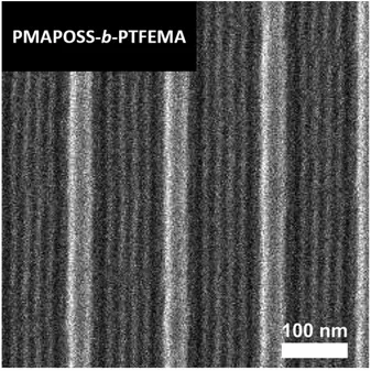
F-containing BCP, poly(polyhedral oligomeric silsesquioxane methacrylate-b-2,2,2-trifluoroethyl methacrylate) (PMAPOSS-b-PTFEMA).98 See Figure 1 above for PTFEMAs molecular structure.
19
shown in the SEM image in Figure 5. In 2019, they reported on the synthesis of PS-b-poly[2-hydroxy-3-(2,2,2-trifluoroethylsulfanyl)propyl methacrylate] (PS-b-PHFMA), and postulated that tuning the γs of the blocks along with annealing conditions provided a route to perpendicular lamellar. Similar to Deng’s work, modest annealing conditions (120°C for 10 mins) were sufficient for PS-b-PHFMA microphase separation, which are extremely attractive for CMOS processing.
Figure 6. Top-down SEM image of aligned PMAPOSS-b-PTFEMA features using graphoepitaxy guiding stripes with an L0 = 15 nm. Image reproduced with permission from American Chemical
Society.98
Modifications of fluorinated BCP blocks have also been reported to significantly enhance χ values. Ryu and co-workers reported on the synthesis of PS-b-poly-(2,2,2-trifluoroethyl acrylate) (PS-b-PTFEAs) BCPs with sub-15 nm L0.99 PTFEMA’s molecular structure is shown in Figure 1. This
was feasible following high-conversion transesterification in acrylate units of PS-b-poly (tert-butyl acrylate) materials. The process allowed the retention of low Đ values and uniform patterning atop a mat layer despite significant γs differences between blocks. In our group, we have synthesized via RAFT a series of high χ-low N PS-b-poly(2-fluoro ethyl methylacrylate) (PS-b-P2FEMA)
20
BCPs.100 There are two significant advantages of this new F-BCP. Firstly, since P2FEMA only
possesses one fluorine atom, large scale dewetting does not present and perpendicular lamellar features with sub-10 nm CD are possible. Secondly, as P2FEMA exhibits similar characteristics to PMMA, the possibility to etch or chemically modify P2FEMA using sequential infiltration synthesis101 (i.e. replication of BCP features through selective impregnation of BCP domains using
atomic layer deposition) is feasible to produce hard mask features.
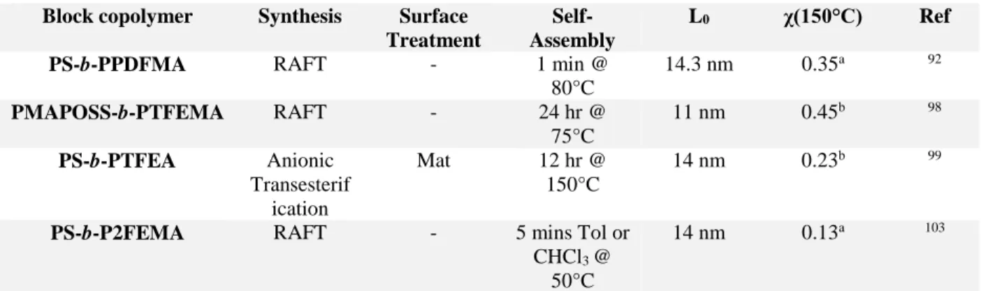
Table 3. Summary of fluorine containing BCPs and corresponding synthesis, L0, and χ. Molecular
structures of fluorine blocks are shown in Figure 1. aEstimated using a reference volume of 118 Å3. bEstimated using a reference volume, 𝑉𝑉
𝑟𝑟𝑟𝑟𝑟𝑟 = [(𝑀𝑀𝑎𝑎𝑀𝑀𝑏𝑏)/(𝜌𝜌𝑎𝑎𝜌𝜌𝑏𝑏)]1/2 with Mi and ρi the
molecular weight of the repeating unit and the density of the block i, respectively.99,102
Block copolymer Synthesis Surface Treatment
Self-Assembly
L0 χ(150°C) Ref PS-b-PPDFMA RAFT - 1 min @
80°C 14.3 nm 0.35a 92 PMAPOSS-b-PTFEMA RAFT - 24 hr @ 75°C 11 nm 0.45b 98 PS-b-PTFEA Anionic Transesterif ication Mat 12 hr @ 150°C 14 nm 0.23b 99
PS-b-P2FEMA RAFT - 5 mins Tol or CHCl3 @
50°C
14 nm 0.13a 103
Despite the long history of using fluorinated polymers in the semiconductor industry,104,105 their
use as BCP etch masks have not been well studied until now. In this section, we have shown the knowledge gained over the past 5 years and the feasibility of F-BCPs as excellent candidates for next-generation sub-10 nm lithography.
5. Beyond PS-b-PMMA through subtle macromolecular engineering
In this section, we summarize novel BCPs reported that allow the formation of aggressive features but do not contain Si- or F- blocks. Once more, we have chosen BCPs that have specific attributes
21
and place them as practical candidates for advanced lithography. We particularly focus on BCPs that align well with standard PS-b-PMMA practices, i.e. thermal annealing and chemoepitaxy compatibility.
5.1 Systems derived from PS-b-PMMA architecture
Ji’s group have exemplified viable routes to PMMA like blocks to pattern ultra-low dimensions. For example, using PS-b-poly (methylacrylate) (PS-b-PMA) which possesses a χ value of 0.068 (i.e. twice that of PMMA), they demonstrated aligned line structures (via chemoepitaxy). Moreover, PS-b-PMA L0 values of 14.6 nm were possible over large areas after thermal annealing
alone (see PMA molecular structure in Figure 1 and PS-b-PMA self-assembled patterns in Figure 6a).106 Critically, PMA possesses a similar block γs to PMMA enabling perpendicular lamellar
orientation with the appropriated surface and bake conditions. Ji and co-workers also showed a similar patterning strategy using PS‑b-poly(lactic acid-alt-glycolic acid) (PS-b-PLGA), that exhibits similar wetting behavior to PS-b-PMMA and PS-b-PLGA was also integrated in a chemoepitaxy flow.107 PLGA possesses one methyl group less than the well-studied
PS-b-PLA BCP system,108,109,110 but holds a very high χ of 0.155, and in this study impressively
patterned features with L0 = 15.5 nm.
While the above examples show methods to make PMMA like blocks, it is worth noting the ongoing efforts to further push PS-b-PMMA BCPs to sub-20 nm L0. For example, Yoshida et al.
reported a novel post-polymerization modification of PS-b-PMMA films with ester/amide linkages.111 The authors achieved an L
0 as low as 18 nm in thin films with sub-10 nm CDs in
guiding templates. Others have used small amounts of ionic liquid added to lamellar PS-b-PMMA to pattern L0 = 16.5 nm with CD less than 8.5 nm.112 More recently, Woo et al. demonstrated a
22
clever synthetic strategy by adding a short mid-block, poly(methacrylic acid) (PMAA) between PS and PMMA to form the tri-BCP PS-b-PMAA-b-PMMA. The PMAA addition led to the production of patterns with an L0 of 16.7 nm but importantly balanced block interactions and
enabled perpendicular feature orientation.113 The above examples provide a view of ways in which
researchers can now engineer new block chemistry, as well as PMMA blocks in order to push L0
and CD values to ever smaller dimensions.
Russell and co-workers have reported on the applicability of poly (solketal methacrylate)-b-PS (PS) BCP systems to self-assemble with ultra-low dimensions. They introduced PSM-b-PS in 2017 describing the acid hydrolysis of the PSM-b-PSM block to poly (glycerol monomethacrylate) (PGM).114 This initial work examined the bulk phase behavior of PGM-b-PS producing 5.4 nm L
0
with sub-3 nm microdomains. Importantly, they have further characterized the behavior of
PSM-b-PS in thin film form.115 A lamellar L0 of 9.8 nm can be realized in thin films (see Figure 6b),
however one must note that an acid must be used for solvent vapor annealing (for the PSM to PGM transformation). Additionally, a lengthy thermal anneal is required that could be problematic for manufacturing, thus more practical annealing protocols for PSM-b-PS are needed. A similar remark can be made on recent work by Sweat et al. following synthesis of poly(4-tert-butylstyrene)-b-P2VP (P(tBuSt)-b-P2VP) BCPs that possessed a relatively high χ (0.11 @ 150°C, based on a reference volume of 118 Å3).116 Despite achieving sub-10 nm CD with
23
Table 4. Summary of BCPs in Section 5 and corresponding synthesis, L0, and χ. aEstimated using
a reference volume of 118 Å3. bReference volume calculated using 𝑉𝑉
𝑟𝑟𝑟𝑟𝑟𝑟 = [(𝑀𝑀𝑎𝑎𝑀𝑀𝑏𝑏)/(𝜌𝜌𝑎𝑎𝜌𝜌𝑏𝑏)]1/2
. See note and reference for table 3 above. Block
copolymer
Synthesis Surface Treatment
Self-Assembly L0 χ(150°C) Ref PS-b-PMA RAFT Mat 3 min @ 80°C 14.6 nm 0.068a 106 PGM-b-PS RAFT PSM-r-PS SVA 80 mins 12
hrs @ 150 °C
9.8 nm 0.40a 115,117
PDHS-b-PS RAFT - 12 hrs @ 170°C 8.8 nm 0.72b 118
Figure 6. (a) Top-down SEM image of a lamellar PS-b-PMA BCP pattern on a homopolymer mat, (b) Top-down image of a lamellar PSM-b-PS BCP exposed to trifluoroacetic acid vapor after thermal annealing and etching process (scale bar: 200 nm) and (c) AFM image after PDHS-b-PS self-assembly with sub-10 nm L0. All images reproduced with permission from American
Chemical Society106,115 ,118
Another promising class of high-χ BCP materials center on hydroxystyrene based BCPs (Figure 1 shows the chemical structure of di-hydroxystyrene). Reports have disclosed several efforts achieving sub-16 nm L0 in thin film form including PDHS-b-PS (see Figure 6c),15
P3HS-b-PDMS,119 as well as P3HS-b-P(tBuSt) and P4HS-b-P(tBuSt).120
(c)
(a)
PGM-b-PS
L
0= 9.8 nm
(b)
PDHS-b-PS
L
0= 8.8 nm
PS-b-PMA
L
0= 14.6 nm
24
6. “Advanced” BCP architectures
6.1. Biobased BCPs
Numerous efforts have also been made to create biomass-based BCPs, offering a greener alternative than oil-based monomers. Borsali and co-workers have made impressive strides in the use of maltoheptaose (MH) oligomer (see MH molecular structure in Figure 1). The strong hydrophilicity brought by the presence of numerous alcohol functions associated with the rod-like structure of oligosaccharides oligomers produce high-χ BCP materials when linked to organic polymers. The group proposed BCPs comprising polystyrene and maltoheptaose (PS-b-MH) synthesized by coupling azide-functionalized PS and alkyne-functionalized MH via click chemistry. PS-b-MH showed a cylindrical structure in thin film and bulk with an L0 of 10 nm
demonstrated by AFM and SAXS analysis.121,122,123 For lithographic applications, the group also
studied the etching contrast between MH and PS and showed that MH is 14 times more selective than PS over CF4 etching thus demonstrating good etch selectivity.124 Concerning etching contrast,
silylated blocks were also used in order to create hard mask features. Etching PTMSS-b-MH BCP synthesized by ATRP and azide-alkyne click chemistry showed a very good selectivity, etching MH block 28 times faster than PTMSS. Such BCPs maybe a viable semiconductor option in the future if materials can be sourced at low cost and for the technical aspects (small L0,high etch
selectivity) discussed above.
6.2 Bottlebrush BCPs
Complex BCP architectures can also open new opportunities for BCP nanomanufacturing for patterning ultra-low dimensions. For example, synthetic advances in the macromolecular engineering of bottlebrush BCPs (bBCPs) via ROMP of macro-monomers initiated by Grubbs and
25
co-workers were leveraged for the synthesis of well-defined diblock bottlebrush BCPs (An-b-Bm
bBCPs) with narrow dispersity.125 Due to the strong steric hindrance produced by the densely
grafted polymeric chains, An-b-Bm bBCPs exhibit an extended backbone configuration reducing
chain entanglements which subsequently increases self-assembly kinetics.126 Accordingly, An
-b-Bm bBCPs were initially designed to tackle the formation of large periodic nanopatterns for
photonics due to a close to linear relationship between the backbone degree of polymerization and the L0 produced through self-assembly.127,128 Interestingly, symmetric An-b-Bm bBCPs tend to
form lamellar micro-domains oriented perpendicular to the substrate, which is a strong asset for patterning logic features. The perpendicular configuration of symmetric An-b-Bm bBCPs is
believed to result in an entropy gain related to chain-ends effect and a favorable parallel orientation of the rigid backbone.129
A related architecture benefiting the formation of small periodic morphologies and the thesis of this review is the so-called A-branch-B Janus structure (A-branch-B bBCPs). Pioneering works by Johnson and co-workers demonstrated how A-branch-B bBCPs enriches the phase diagram with reports of morphologies with extended interface curvature (i.e. gyroid or HCP cylinders).130
Indeed, the formation of lamellar structures is highly favored for An-b-Bm bBCPs due to the
stretched-out conformation of the backbone segments localized at the A/B interface.131 In contrast
to the An-b-Bm bBCP architecture, the entire bBCP backbone serves as an interface of the
self-assembled structures and the L0 subsequently scales with the A-b-B macromonomer degree of
polymerization allowing the design of ultra-low periodic patterns. Interestingly, it is believed that the preorganization inherent to the A-branch-B bBCP architecture even allows the segregation for χN values lower than that of the parent A-b-B macromonomer underlining the interest of such macromolecular structure for ultra-low dimension patterning.132,133 Accordingly, Cheng et al.
26
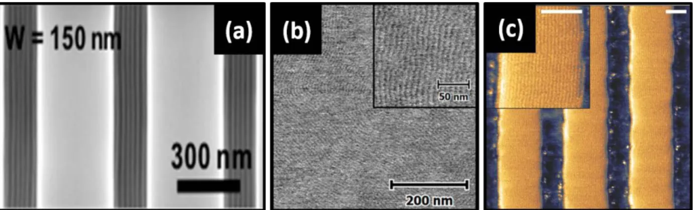
demonstrated how PS-branch-PDMS bBCPs can be integrated with DSA methodologies for the formation of line space patterns from an array of cylindrical PDMS micro-domains with a period of 24 nm while the lack of entanglements promotes chain mobility and efficient phase separation (see Figure 7a below).134
Figure 7. Examples beyond linear di-BCPs (a) Top-down SEM image of well-aligned PS-branch-PDMS bBCP features in trenches of 100 nm depth and width of 150 nm showing out-of-plane PDMS cylinders with L0 ~ 20 nm.134 (b) AFM image of a block co-oligomer (OMDS-b-OLA)
possessing L0 ~ 9.1 nm.57 Images in (a) and (b) reproduced with permission from American
Chemical Society. (c) AFM phase image showing liquid crystal line space patterns with L0 ~ 4.3
nm in DSA trenches with 100 nm width.135 The liquid crystal is based upon oligo(dimethylsiloxane), see text for further details. Scale bars are 50 nm. Image reproduced with permission from Wiley.
6.3 Star BCPs
Star-BCPs are another class of interest for ultralow patterning applications. In addition to providing extensive morphological diversity with respect to linear BCPs, exquisite demonstrations of both smaller CD and architecture-induced orientation with respect to analogous BCPs have been reported in the literature. For example, Minehara et al. used Y-shaped PDMS-b-(PLA)2 BCPs to
tailor both morphology and CD in self-assembled thin films.136 Indeed, the Y-shaped
27
weaker for systems with high segregation strength due to pronounced chain stretching at the domain interface. Another demonstration of interest for patterning applications was recently proposed by Lo et al. with a controlled orientational behavior dictated by an arm star-block architecture through an entropic effect.137 Using an incompatible system based on PS and PDMS,
perpendicularly oriented cylindrical and lamellar nanostructures were achieved in spite of the high surface tensions difference between PS and PDMS. The entropic-based mechanism leading to the preferential orientation of the BCP domains was directly related to the topology of arm star-BCPs with a driving force strongly correlated to the number of arms. As a demonstration of their potential use for nanofabrication, nanoporous PS monoliths with an L0 of 20 nm were produced by
combining plasma etching and wet chemistry. Huang et al. progressed further in the design of star architecture targeting ultra-low dimensions by studying the self-assembly behavior of multi-headed giant surfactants based on the association of multiple polyhedral oligomeric silsesquioxane cages with a PS block.138 In particular, they demonstrated how highly asymmetric lamellar
structures could be produced with periods as low as 7.4 nm. Despite the lack of thin film demonstrations, such asymmetric architectures designed by well-controlled synthetic procedures hold promise for the further development of sub-10 nm patterning.
6.4 Block co-oligomers
To reach incredibly small CD, block co-oligomers have been recently under scrutiny. Siepmann and co-workers explored the limit of segregated systems and conceptualized the perfect system leading to the smallest CD possible using computational simulations.139,140 Amphiphilic block
co-oligomers that act in the boundaries between nonionic surfactants and BCPs were calculated to form lamellae and cylinders domain size as small as 3 and 2.1 nm, respectively. Adapting mean
28
field theory to block co-oligomers led to an interaction parameter χ value of 4.3 at 150°C which is 6 times greater than PS-b-PDHS, one of the highest reported value for BCPs. A variety of block co-oligomer systems have been reported and novel design rules are expected to emerge from these pioneering works. Meijer and co-workers proposed coupling strategies involving dimethylsiloxane and lactic acid blocks.57 The controlled synthesis allowed the fabrication of discrete block co-oligomers ODMS-b-OLA showing a Ɖ very close to unity. Impressively, in comparison to disperse BCPs obtained using the ROP of lactide with a hydroxyl-terminated PDMS macro-initiator, they exhibited quicker self-assembly with L0 as low as 9.1 nm demonstrated (see Figure 7b).
Interestingly, the overall degree of ordering was shown to be increased for discrete oligomers and d-spacing was observed to be smaller, possibly because of a better intermolecular packing in the self-assembled structures. Additionally, the TODT of segregated structures obtained from disperse
oligomers were observed to be higher, suggesting more stability for lower χN values. However, an accompanying work from Hawker and co-workers showed an opposite trend in the TODT behavior
for ODMS-b-OMMA. The authors reported that disperse block co-oligomers exhibited lower TODT
than the discrete analogues.141 The contrasting reports on block co-oligomers infers the phase
behavior of very low-N BCPs is not yet fully understood and that the effect of end-groups, block junctions, intermolecular interactions and non-idealities (conformational asymmetry, validity of Gaussian chain statistics at N → 1) must be strongly considered.
Consequently, discrete polymers are still undergoing scrutiny to reach the limits of high χ-low N BCPs. Nevertheless, the progress in the controlled synthesis of block co-oligomers allows the study of the dispersity effect on self-assembly, thus opening a new research field that will enable possible realization of theoretical works. Indeed, novel synthetic strategies will be required to continually reduce BCP dimensions.
29
6.5 Liquid crystalline BCPs
Rod-coil BCPs bearing liquid crystalline mesogens (LC-BCPs) have also been proposed as a promising alternative to coil-coil BCPs to target sub-10 nm CD. In addition to the Flory-Huggins interaction parameter, two additional driving forces are at play in the segregation behavior of LC-BCPs: the LC orientational ordering inside the rod blocks and the conformational geometric asymmetry between the rod and coil blocks. As a result, LC-BCPs exhibit strong phase separation tendency which further accentuates the Flory-Huggins chemical incompatibility (χN(rod-coil BCPs)≥
5 versus χN(coil-coil BCPs) ≥ 10.5).142 Additionally, an appropriate choice of stimuli-responsive
mesogens can be further employed to control the ordering of the resulting nanostructure; an important feature for DSA. As an example, the Ikeda and Seki groups demonstrated how LC-BCP thin films can be aligned by using a linearly polarized light to directionally orient azo-mesogens.143,144 Two particular LC systems have been reported for patterning applications: a
photoresponsive LC azo rigid core tailed by oligo(dimethylsiloxanes) (ODMS-b-AzoLC-b-ODMS)135,145 and a mesogen-jacketed LC
PDMS-b-poly(2,5-bis[(4-methoxyphenyl)-(oxycarbonyl]styrene) (PDMS-b-PMPCS).146,147 ODMS-b-AzoLC-b-ODMS and
PDMS-b-PMPCS were both integrated via common DSA topographical methods leading to well-aligned line and space arrays. Figure 7c shows an AFM image of remarkably well-defined line space features of 4.3 nm period from ODMS-b-AzoLC-b-ODMS. The above LC systems may provide the required etching contrast due to the presence of an inorganic component, i.e. ODMS. However, the sensitivity of LC systems to external stimuli is an issue, and may cause problems for integrating in common CMOS processing with multiple plasma etching steps and high temperature anneals.
30
7. Summary and outlook
Progress of high χ–low N BCP synthesis and manipulation in thin films has enabled sub-16 nm L0
and sub-8 nm CD across many diverse BCP systems as discussed here. It is also apparent that many variables ranging from polymer synthesis conditions, surface and interface behavior, as well as CMOS integration feasibility must be satisfied to produce BCP relevant patterns for logic applications. In the past 5 years, tremendous efforts in the BCP-DSA field have now realized 10 nm L0 and sub-5 nm CD.
So, what is next? Expanding our ability to engineer BCPs and dial-in specific chemistry is a critical determinant for our advances in ultra-low dimensional patterning, as highlighted through our examination of bottlebrush, star, and rod coil liquid crystalline BCPs in section 5. Given that most reports in section 6 are the first of their kind, these systems may see the greatest attention in the near future for ultra-low patterning. Recently, Armes and co-workers described a robust methodology that may prove useful for future sub-10 nm scaling research.148 The authors reported
the benefits of using polymerization induced self-assembly (PISA)149 for the preparation of high χ–low N BCPs. The nanoparticle formed by the BCPs chains during the PISA process allow a pre-organization at the molecular scale leading to rapid self-assembly unlike molecularly dissolved polymer chains. While thin film processing was not explored in-depth, the ability to control the initial ordering state of the BCP chains with PISA could be a promising platform for future research efforts. It is noteworthy that further experimental and theoretical analysis is crucial to opening up this platform, as one must also consider the out-of-equilibrium nature of the kinetically trapped structures formed by PISA.
31
An even more holistic approach must be taken in future work given the knowledge we now possess. Such approaches would encompass all aspects of the process from synthesis to thin film processing to electrical characterization of Si nanofins or other semiconductor surfaces, melding both academic and industry partner strengths. To date, few studies exist that analyze device performance from BCP derived features.150,151 For example, the nature of the Si-BCP and F-BCP
materials described in this review may also find more diverse applications on future devices that integrate logic and memory. Both Si and F material layers have been utilized in the semiconductor for decades. SiOx layers and features can be readily formed from Si-BCPs outlined above through
plasma etching while the host of F-BCPs now available may find use in various back-end-of-line (BEOL) needs.
Corresponding Authors
*E-mail:
C.C. - [email protected] G.F. - [email protected]
The authors declare no competing financial interest. Funding Information & Acknowledgements
The authors are sincerely grateful for financial support from the University of Bordeaux and the LabEx AMADEus (ANR-10-LABEX-0042-AMADEUS). The authors also thank the LCPO support staff: Aude Manson, Melanie Bousquet, Ellena Karnezis, and Gilles Pecastaings for their endless everyday help.
32
7. References
1. G. E. Moore, Electronics, 1965, 38, 114-117.
2. L. Li, X. Liu, S. Pal, S. Wang, C. K. Ober and E. P. Giannelis, Chemical Society Reviews, 2017. 3. S. Salahuddin, K. Ni and S. Datta, Nature Electronics, 2018, 1, 442-450.
4. A. P. Jacob, R. Xie, M. G. Sung, L. Liebmann, R. T. P. Lee and B. Taylor, International Journal of High
Speed Electronics and Systems, 2017, 26, 1740001.
5. in Fundamentals and Applications of Nano Silicon in Plasmonics and Fullerines, ed. M. Nayfeh, Elsevier, 2018, pp. 89-137.
6. G. Rhys Alun, W. Aled, O. Chloe, R. Jonathan, V. Aravind and T. Thomas, Journal of Physics D:
Applied Physics, 2013, 46, 503001.
7. R. Lundy, S. P. Flynn, C. Cummins, S. M. Kelleher, M. N. Collins, E. Dalton, S. Daniels, M. A. Morris and R. Enright, Physical Chemistry Chemical Physics, 2017, 19, 2805-2815.
8. S.-J. Jeong, J. Y. Kim, B. H. Kim, H.-S. Moon and S. O. Kim, Materials Today, 2013, 16, 468-476. 9. H. Hu, M. Gopinadhan and C. O. Osuji, Soft Matter, 2014, 10, 3867-3889.
10. J. L. Harry, Proc.SPIE, 2019.
11. Y. Yang, Y. Li, Q. Wu, J. Zhu and S. CHen, Journal of Microelectronic Manufacturing, 2020, 3. 12. M. Nihar, F. Elliott, L. Eric, R. Angelique, S. Jeffrey, F. Richard, W. Mingmei, I. Kiyohito, D. Sanjana,
K. Akiteru, K. Kaushik, R. Alok, O. M. David, N. Kenjiro, S. Steven, D. Anton and B. Peter, Proc.SPIE, 2015.
13. Y. Chen, Q. Cheng and W. Kang, Technological merits, process complexity, and cost analysis of
self-aligned multiple patterning, SPIE, 2012.
14. A. P. Lane, X. Yang, M. J. Maher, G. Blachut, Y. Asano, Y. Someya, A. Mallavarapu, S. M. Sirard, C. J. Ellison and C. G. Willson, ACS Nano, 2017, 11, 7656-7665.
15. J. Kwak, A. K. Mishra, J. Lee, K. S. Lee, C. Choi, S. Maiti, M. Kim and J. K. Kim, Macromolecules, 2017, 50, 6813-6818.
16. V. R. Manfrinato, A. Stein, L. Zhang, C.-Y. Nam, K. G. Yager, E. A. Stach and C. T. Black, Nano Letters, 2017, 17, 4562-4567.
17. M. D. Austin, H. Ge, W. Wu, M. Li, Z. Yu, D. Wasserman, S. A. Lyon and S. Y. Chou, Applied Physics
Letters, 2004, 84, 5299-5301.
18. Y. Oktay, B. Elizabeth, H. Rik, M. Marieke, W. Sander, R. Gijsbert, O. Anton van, D. Paul, F. Jo, V. Michaela and E. Yasin, Proc.SPIE, 2017.
19. https://en.ctimes.com.tw/DispNews.asp?O=HK42R15T26CSAA00ND, Accessed May 2020, 2020. 20. M. A. Morris, Microelectronic Engineering, 2015, 132, 207-217.
21. C. Cummins and M. A. Morris, Microelectronic Engineering, 2018, 195, 74-85. 22. C. Yu and X. Shisheng, International Journal of Extreme Manufacturing, 2020.
23. R. A. Segalman, H. Yokoyama and E. J. Kramer, Advanced Materials, 2001, 13, 1152-1155. 24. K. Shin, K. A. Leach, J. T. Goldbach, D. H. Kim, J. Y. Jho, M. Tuominen, C. J. Hawker and T. P. Russell,
Nano Letters, 2002, 2, 933-936.
25. M. P. Stoykovich, M. Müller, S. O. Kim, H. H. Solak, E. W. Edwards, J. J. De Pablo and P. F. Nealey,
Science, 2005, 308, 1442-1446.
26. S. Ji, L. Wan, C.-C. Liu and P. F. Nealey, Progress in Polymer Science, 2016, 54-55, 76-127. 27. M. J. Fasolka and A. M. Mayes, Annual Review of Materials Science, 2001, 31, 323-355. 28. W. Li, P. F. Nealey, J. J. de Pablo and M. Müller, Physical Review Letters, 2014, 113, 168301. 29. S.-M. Hur, V. Thapar, A. Ramírez-Hernández, G. Khaira, T. Segal-Peretz, P. A. Rincon-Delgadillo, W.
Li, M. Müller, P. F. Nealey and J. J. de Pablo, Proceedings of the National Academy of Sciences, 2015, 112, 14144.
33
30. H. S. Wang, K. H. Kim and J. Bang, Macromolecular Rapid Communications, 2019, 40, 1800728. 31. C. Sinturel, F. S. Bates and M. A. Hillmyer, ACS Macro Letters, 2015, 4, 1044-1050.
32. X. Gu, I. Gunkel and T. P. Russell, Philosophical Transactions of the Royal Society A: Mathematical,
Physical and Engineering Sciences, 2013, 371.
33. A. Nunns, J. Gwyther and I. Manners, Polymer, 2013, 54, 1269-1284.
34. M. Ramanathan, Y.-C. Tseng, K. Ariga and S. B. Darling, Journal of Materials Chemistry C, 2013, 1, 2080-2091.
35. C. Sinturel, M. Vayer, M. Morris and M. A. Hillmyer, Macromolecules, 2013, 46, 5399-5415. 36. C. Jin, B. C. Olsen, E. J. Luber and J. M. Buriak, Chemistry of Materials, 2017, 29, 176-188.
37. R. Quirk, in Handbook of Polymer Synthesis, Characterization, and Processing, 2013, pp. 127-162. 38. R. B. Grubbs and R. H. Grubbs, Macromolecules, 2017, 50, 6979-6997.
39. W. J. Durand, G. Blachut, M. J. Maher, S. Sirard, S. Tein, M. C. Carlson, Y. Asano, S. X. Zhou, A. P. Lane, C. M. Bates, C. J. Ellison and C. G. Willson, Journal of Polymer Science Part A: Polymer
Chemistry, 2015, 53, 344-352.
40. J.-S. Wang and K. Matyjaszewski, Journal of the American Chemical Society, 1995, 117, 5614-5615. 41. G. Moad, E. Rizzardo and S. H. Thang, Polymer, 2008, 49, 1079-1131.
42. G. Moad, E. Rizzardo and D. H. Solomon, Macromolecules, 1982, 15, 909-914.
43. M. D. Rodwogin, C. S. Spanjers, C. Leighton and M. A. Hillmyer, ACS Nano, 2010, 4, 725-732. 44. A. Baruth, M. Seo, C. H. Lin, K. Walster, A. Shankar, M. A. Hillmyer and C. Leighton, ACS Applied
Materials & Interfaces, 2014, 6, 13770-13781.
45. F. Kayser, G. Fleury, S. Thongkham, C. Navarro, B. Martin-Vaca and D. Bourissou, Macromolecules, 2018, 51, 6534-6541.
46. K. Matyjaszewski and J. Xia, in Handbook of Radical Polymerization, 2002, pp. 523-628. 47. S. Perrier, Macromolecules, 2017, 50, 7433-7447.
48. D. J. Keddie, G. Moad, E. Rizzardo and S. H. Thang, Macromolecules, 2012, 45, 5321-5342. 49. H. Willcock and R. K. O'Reilly, Polymer Chemistry, 2010, 1, 149-157.
50. G. Moad and E. Rizzardo, in Nitroxide Mediated Polymerization: From Fundamentals to
Applications in Materials Science, The Royal Society of Chemistry, 2016, pp. 1-44.
51. D. J. Nathan, C. Jing, P. Andrew, Y. Wei-Ming, A. L. Richard, M. T. Laren and L. H. Clifford, Proc.SPIE, 2012.
52. R. B. Grubbs, Polymer Reviews, 2011, 51, 104-137.
53. R. Verduzco, X. Li, S. L. Pesek and G. E. Stein, Chemical Society Reviews, 2015, 44, 2405-2420. 54. I. Choinopoulos, Polymers, 2019, 11.
55. H. Uchida, Y. Kabe, K. Yoshino, A. Kawamata, T. Tsumuraya and S. Masamune, Journal of the
American Chemical Society, 1990, 112, 7077-7079.
56. K. Takizawa, H. Nulwala, J. Hu, K. Yoshinaga and C. J. Hawker, Journal of Polymer Science Part A:
Polymer Chemistry, 2008, 46, 5977-5990.
57. B. van Genabeek, B. F. M. de Waal, M. M. J. Gosens, L. M. Pitet, A. R. A. Palmans and E. W. Meijer,
Journal of the American Chemical Society, 2016, 138, 4210-4218.
58. S. Böhme, C. Girardot, J. Garnier, J. Arias-Zapata, S. Arnaud, R. Tiron, O. Marconot, D. Buttard and M. Zelsmann, 2016.
59. K. Brassat and J. K. N. Lindner, Advanced Materials Interfaces, 2020, 7, 1901565.
60. C. M. Bates, M. J. Maher, D. W. Janes, C. J. Ellison and C. G. Willson, Macromolecules, 2013, 47, 2-12.
61. X. Zhang, J. N. Murphy, N. L. Y. Wu, K. D. Harris and J. M. Buriak, Macromolecules, 2011, 44, 9752-9757.
34
63. P. Mokarian-Tabari, C. Cummins, S. Rasappa, C. Simao, C. M. Sotomayor Torres, J. D. Holmes and M. A. Morris, Langmuir, 2014, 30, 10728-10739.
64. C. Cummins, T. Ghoshal, J. D. Holmes and M. A. Morris, Advanced Materials, 2016, 28, 5586-5618. 65. J. G. Kennemur, Macromolecules, 2019, 52, 1354-1370.
66. D. Borah, M. T. Shaw, J. D. Holmes and M. A. Morris, ACS Applied Materials & Interfaces, 2013, 5, 2004-2012.
67. W. I. Park, J. M. Kim, J. W. Jeong and Y. S. Jung, ACS Nano, 2014, 8, 10009-10018.
68. J. W. Jeong, Y. H. Hur, H.-j. Kim, J. M. Kim, W. I. Park, M. J. Kim, B. J. Kim and Y. S. Jung, ACS Nano, 2013, 7, 6747-6757.
69. J. Arias-Zapata, J. D. Garnier, H.-a. Mehedi, A. Legrain, B. Salem, G. Cunge and M. Zelsmann,
Chemistry of Materials, 2019, 31, 3154-3162.
70. J. W. Jeong, W. I. Park, M.-J. Kim, C. A. Ross and Y. S. Jung, Nano Letters, 2011, 11, 4095-4101. 71. J. M. Kim, Y. H. Hur, J. W. Jeong, T. W. Nam, J. H. Lee, K. Jeon, Y. Kim and Y. S. Jung, Chemistry of
Materials, 2016, 28, 5680-5688.
72. C. Reboul, G. Fleury, K. Aissou, C. Brochon, E. Cloutet, C. Nicolet, X. Chevalier, C. Navarro, R. Tiron, G. Cunge and G. Hadziioannou, Self-assembly of Si-containing block copolymers with
high-segregation strength: toward sub-10nm features in directed self-assembly, SPIE, 2014.
73. Y. Luo, D. Montarnal, S. Kim, W. Shi, K. P. Barteau, C. W. Pester, P. D. Hustad, M. D. Christianson, G. H. Fredrickson, E. J. Kramer and C. J. Hawker, Macromolecules, 2015, 48, 3422-3430.
74. J. Cushen, L. Wan, G. Blachut, M. J. Maher, T. R. Albrecht, C. J. Ellison, C. G. Willson and R. Ruiz,
ACS Applied Materials & Interfaces, 2015, 7, 13476-13483.
75. C. M. Bates, T. Seshimo, M. J. Maher, W. J. Durand, J. D. Cushen, L. M. Dean, G. Blachut, C. J. Ellison and C. G. Willson, Science, 2012, 338, 775-779.
76. J. D. Cushen, I. Otsuka, C. M. Bates, S. Halila, S. Fort, C. Rochas, J. A. Easley, E. L. Rausch, A. Thio, R. Borsali, C. G. Willson and C. J. Ellison, ACS Nano, 2012, 6, 3424-3433.
77. J. D. Cushen, C. M. Bates, E. L. Rausch, L. M. Dean, S. X. Zhou, C. G. Willson and C. J. Ellison,
Macromolecules, 2012, 45, 8722-8728.
78. K. Aissou, M. Mumtaz, G. Fleury, G. Portale, C. Navarro, E. Cloutet, C. Brochon, C. A. Ross and G. Hadziioannou, Advanced Materials, 2015, 27, 261-265.
79. Y. Rho, K. Aissou, M. Mumtaz, W. Kwon, G. Pécastaings, C. Mocuta, S. Stanecu, E. Cloutet, C. Brochon, G. Fleury and G. Hadziioannou, Small, 2015, 11, 6377-6383.
80. A. Legrain, G. Fleury, M. Mumtaz, C. Navarro, J. Arias-Zapata, X. Chevalier, I. Cayrefourcq and M. Zelsmann, ACS Applied Materials & Interfaces, 2017, 9, 43043-43050.
81. K. Aissou, W. Kwon, M. Mumtaz, S. Antoine, M. Maret, G. Portale, G. Fleury and G. Hadziioannou,
ACS Nano, 2016, 10, 4055-4061.
82. K. Aissou, M. Mumtaz, A. Alvarez-Fernandez, J. Mercat, S. Antoine, G. Pécastaings, V. Ponsinet, C. Dobrzynski, G. Fleury and G. Hadziioannou, Macromolecular Rapid Communications, 2018, 39, 1700754.
83. K. Aissou, M. Mumtaz, P. Marcasuzaa, C. Brochon, E. Cloutet, G. Fleury and G. Hadziioannou,
Small, 2017, 13, 1603184.
84. C. Cummins, A. Gangnaik, R. A. Kelly, D. Borah, J. O'Connell, N. Petkov, Y. M. Georgiev, J. D. Holmes and M. A. Morris, Nanoscale, 2015.
85. C. Cummins, A. Gangnaik, R. A. Kelly, A. J. Hydes, J. O’Connell, N. Petkov, Y. M. Georgiev, D. Borah, J. D. Holmes and M. A. Morris, Chemistry of Materials, 2015, 27, 6091-6096.
86. C. Cummins, R. A. Kelly, A. Gangnaik, Y. M. Georgiev, N. Petkov, J. D. Holmes and M. A. Morris,
Macromolecular Rapid Communications, 2015, 36, 762-767. 87. G. Blachut, PhD Thesis, 2016, Accessed May 2020.
35
89. M. A. Hillmyer and T. P. Lodge, Journal of Polymer Science Part A: Polymer Chemistry, 2002, 40, 1-8.
90. Y. Ren, T. P. Lodge and M. A. Hillmyer, Macromolecules, 2000, 33, 866-876.
91. S. Zhu, W. F. Edmonds, M. A. Hillmyer and T. P. Lodge, Journal of Polymer Science Part B: Polymer
Physics, 2005, 43, 3685-3694.
92. X. Li, J. Li, C. Wang, Y. Liu and H. Deng, Journal of Materials Chemistry C, 2019, 7, 2535-2540. 93. H. Cao, X. Li, Y. Liu and H. Deng, Journal of Photopolymer Science and Technology, 2019, 32,
413-416.
94. C. Wang, X. Li and H. Deng, ACS Macro Letters, 2019, 8, 368-373.
95. A. Cintora, H. Takano, M. Khurana, A. Chandra, T. Hayakawa and C. K. Ober, Polymer Chemistry, 2019, 10, 5094-5102.
96. A. Chandra, R. Nakatani, T. Uchiyama, Y. Seino, H. Sato, Y. Kasahara, T. Azuma and T. Hayakawa,
Advanced Materials Interfaces, 2019, 6, 1801401.
97. R. Nakatani, A. Chandra, T. Uchiyama, Y. Nabae and T. Hayakawa, ACS Macro Letters, 2019, 8, 1122-1127.
98. R. Nakatani, H. Takano, A. Chandra, Y. Yoshimura, L. Wang, Y. Suzuki, Y. Tanaka, R. Maeda, N. Kihara, S. Minegishi, K. Miyagi, Y. Kasahara, H. Sato, Y. Seino, T. Azuma, H. Yokoyama, C. K. Ober and T. Hayakawa, ACS Applied Materials & Interfaces, 2017, 9, 31266-31278.
99. S. Jo, S. Jeon, T. Jun, C. Park and D. Y. Ryu, Macromolecules, 2018, 51, 7152-7159.
100. C. Cummins, D. Mantione, F. Cruciani, G. Pino, N. Demazy, Y. Shi, G. Portale, G. Hadziioannou and G. Fleury, Macromolecules, 2020.
101. A. Singh, W. Knaepen, S. Sayan, Z. el Otell, B. T. Chan, J. W. Maes and R. Gronheid, 2015.
102. W. Zha, C. D. Han, D. H. Lee, S. H. Han, J. K. Kim, J. H. Kang and C. Park, Macromolecules, 2007, 40, 2109-2119.
103. C. Cummins and e. al., Unpublished Work, 2020.
104. M. Rothschild, T. M. Bloomstein, T. H. Fedynyshyn, V. Liberman, W. Mowers, R. Sinta, M. Switkes, A. Grenville and K. Orvek, Journal of Fluorine Chemistry, 2003, 122, 3-10.
105. S. Krishnan, Y.-J. Kwark and C. K. Ober, The Chemical Record, 2004, 4, 315-330. 106. Y. Pang, X. Jin, G. Huang, L. Wan and S. Ji, Macromolecules, 2019, 52, 2987-2994. 107. X. Zhang, Q. He, Q. Chen, P. F. Nealey and S. Ji, ACS Macro Letters, 2018, 7, 751-756.
108. C. Sinturel, D. Grosso, M. Boudot, H. Amenitsch, M. A. Hillmyer, A. Pineau and M. Vayer, ACS
Applied Materials & Interfaces, 2014, 6, 12146-12152.
109. C. Cummins, P. Mokarian-Tabari, P. Andreazza, C. Sinturel and M. A. Morris, ACS Applied Materials
& Interfaces, 2016, 8, 8295-8304.
110. I. Keen, H.-H. Cheng, A. Yu, K. S. Jack, T. R. Younkin, M. J. Leeson, A. K. Whittaker and I. Blakey,
Macromolecules, 2013, 47, 276-283.
111. K. Yoshida, L. Tian, K. Miyagi, A. Yamazaki, H. Mamiya, T. Yamamoto, K. Tajima, T. Isono and T. Satoh, Macromolecules, 2018, 51, 8064-8072.
112. X. Chen, C. Zhou, S.-J. Chen, G. S. W. Craig, P. Rincon-Delgadillo, T. Dazai, K. Miyagi, T. Maehashi, A. Yamazaki, R. Gronheid, M. P. Stoykovich and P. F. Nealey, ACS Applied Materials & Interfaces, 2018, 10, 16747-16759.
113. S. Woo, S. Jo, D. Y. Ryu, S.-H. Choi, Y. Choe, A. Khan, J. Huh and J. Bang, ACS Macro Letters, 2017, 6, 1386-1391.
114. G. Jeong, D. M. Yu, J. K. D. Mapas, Z. Sun, J. Rzayev and T. P. Russell, Macromolecules, 2017, 50, 7148-7154.
115. D. M. Yu, D. M. Smith, H. Kim, J. K. D. Mapas, J. Rzayev and T. P. Russell, Macromolecules, 2019, 52, 3592-3600.
36
116. D. P. Sweat, M. Kim, S. R. Larson, J. W. Choi, Y. Choo, C. O. Osuji and P. Gopalan, Macromolecules, 2014, 47, 6687-6696.
117. D. M. Yu, J. K. D. Mapas, H. Kim, J. Choi, A. E. Ribbe, J. Rzayev and T. P. Russell, Macromolecules, 2018, 51, 1031-1040.
118. J. Kwak, A. K. Mishra, J. Lee, K. S. Lee, C. Choi, S. Maiti, M. Kim and J. K. Kim, Macromolecules, 2017.
119. K. Azuma, J. Sun, Y. Choo, Y. Rokhlenko, J. H. Dwyer, B. Schweitzer, T. Hayakawa, C. O. Osuji and P. Gopalan, Macromolecules, 2018, 51, 6460-6467.
120. C. Kanimozhi, M. Kim, S. R. Larson, J. W. Choi, Y. Choo, D. P. Sweat, C. O. Osuji and P. Gopalan, ACS
Macro Letters, 2016, 5, 833-838.
121. I. Otsuka, S. Tallegas, Y. Sakai, C. Rochas, S. Halila, S. Fort, A. Bsiesy, T. Baron and R. Borsali,
Nanoscale, 2013, 5, 2637-2641.
122. Y. Liao, W.-C. Chen and R. Borsali, Advanced Materials, 2017, 29, 1701645.
123. Y. Liao, K. Liu, W.-C. Chen, B. Wei and R. Borsali, Macromolecules, 2019, 52, 8751-8758.
124. I. Otsuka, N. Nilsson, D. B. Suyatin, I. Maximov and R. Borsali, Soft Matter, 2017, 13, 7406-7411. 125. Y. Xia, B. D. Olsen, J. A. Kornfield and R. H. Grubbs, Journal of the American Chemical Society, 2009,
131, 18525-18532.
126. W. Gu, J. Huh, S. W. Hong, B. R. Sveinbjornsson, C. Park, R. H. Grubbs and T. P. Russell, ACS Nano, 2013, 7, 2551-2558.
127. M. B. Runge and N. B. Bowden, Journal of the American Chemical Society, 2007, 129, 10551-10560. 128. B. R. Sveinbjoernsson, R. A. Weitekamp, G. M. Miyake, Y. Xia, H. A. Atwater and R. H. Grubbs,
Proceedings of the National Academy of Sciences of the United States of America, 2012, 109, 14332-14336.
129. S. W. Hong, W. Gu, J. Huh, B. R. Sveinbjornsson, G. Jeong, R. H. Grubbs and T. P. Russell, ACS Nano, 2013, 7, 9684-9692.
130. K. Kawamoto, M. Zhong, K. R. Gadelrab, L.-C. Cheng, C. A. Ross, A. Alexander-Katz and J. A. Johnson, Journal of the American Chemical Society, 2016, 138, 11501-11504.
131. J. Rzayev, Macromolecules, 2009, 42, 2135-2141.
132. Z.-H. Guo, A. N. Le, X. Feng, Y. Choo, B. Liu, D. Wang, Z. Wan, Y. Gu, J. Zhao, V. Li, C. O. Osuji, J. A. Johnson and M. Zhong, Angewandte Chemie International Edition, 2018, 57, 8493-8497.
133. H. V. T. Nguyen, N. M. Gallagher, F. Vohidov, Y. Jiang, K. Kawamoto, H. Zhang, J. V. Park, Z. Huang, M. F. Ottaviani, A. Rajca and J. A. Johnson, ACS Macro Letters, 2018, 7, 472-476.
134. L.-C. Cheng, K. R. Gadelrab, K. Kawamoto, K. G. Yager, J. A. Johnson, A. Alexander-Katz and C. A. Ross, Nano Letters, 2018, 18, 4360-4369.
135. K. Nickmans, J. N. Murphy, B. de Waal, P. Leclère, J. Doise, R. Gronheid, D. J. Broer and A. P. H. J. Schenning, Advanced Materials, 2016, 28, 10068-10072.
136. H. Minehara, L. M. Pitet, S. Kim, R. H. Zha, E. W. Meijer and C. J. Hawker, Macromolecules, 2016, 49, 2318-2326.
137. T.-Y. Lo, A. Dehghan, P. Georgopanos, A. Avgeropoulos, A.-C. Shi and R.-M. Ho, Macromolecules, 2016, 49, 624-633.
138. M. Huang, K. Yue, J. Huang, C. Liu, Z. Zhou, J. Wang, K. Wu, W. Shan, A.-C. Shi and S. Z. D. Cheng,
ACS Nano, 2018, 12, 1868-1877.
139. Q. P. Chen, L. Barreda, L. E. Oquendo, M. A. Hillmyer, T. P. Lodge and J. I. Siepmann, ACS Nano, 2018, 12, 4351-4361.
140. L. Barreda, Z. Shen, Q. P. Chen, T. P. Lodge, J. I. Siepmann and M. A. Hillmyer, Nano Letters, 2019, 19, 4458-4462.