HAL Id: hal-01020992
https://hal.archives-ouvertes.fr/hal-01020992v2
Submitted on 8 Feb 2015
HAL is a multi-disciplinary open access
archive for the deposit and dissemination of
sci-entific research documents, whether they are
pub-lished or not. The documents may come from
teaching and research institutions in France or
abroad, or from public or private research centers.
L’archive ouverte pluridisciplinaire HAL, est
destinée au dépôt et à la diffusion de documents
scientifiques de niveau recherche, publiés ou non,
émanant des établissements d’enseignement et de
recherche français ou étrangers, des laboratoires
publics ou privés.
Architecture for Aeronautics Applications
Claude Vanhecke, Laurent Assouère, Anqing Wang, Paul Durand-Estèbe,
Fabrice Caignet, Jean-Marie Dilhac, Marise Bafleur
To cite this version:
Claude Vanhecke, Laurent Assouère, Anqing Wang, Paul Durand-Estèbe, Fabrice Caignet, et al..
Multisource and Battery-free Energy Harvesting Architecture for Aeronautics Applications. IEEE
Transactions on Power Electronics, Institute of Electrical and Electronics Engineers, 2015, 30 (6),
pp.3215-3227. �10.1109/TPEL.2014.2331365�. �hal-01020992v2�
Abstract— We suggest an innovative architecture for an efficient energy generator devoted to the powering of a wireless sensor network deployed for Aircraft Health Monitoring. This battery-free generator captures energy from its environment (transient thermal gradients as a main source, and vibrations as a secondary source allowing early biasing of the generator) and stores this energy in ultracapacitors. In this way, this multi-source architecture benefits from the synergy between energy scavenging and harvesting: vibrations bring low but early and permanent energy. They also contribute to energy harvesting during cruise while thermal gradients have vanished. The use of active diodes and of a very low bias current of 10nA/branch allow achieving ultra-low power consumption, experimentally demonstrated on two different CMOS technologies. It is also proven that enough energy could be delivered to power the functions of a wireless sensor node.
Index Terms—Energy harvesting, energy scavenging, structural health monitoring, ultra low-power converter, multisource harvesting, battery-free, nanowatt voltage reference.
I. INTRODUCTION
o address the challenges related to the expansion of air traffic, to the dramatic increase of jet fuel price, and to environmental concerns, the aeronautics industry is seeking technological and process innovations in aircraft maintenance. In this context, Aircraft Health Monitoring (AHM) is one of the major challenges faced by aircraft manufacturers [1, 2].
Main applications of AHM are the airframe, the main engines and the main systems (such as Auxiliary Power Unit - APU), all major contributors to Aircraft “Delay and Cancellation”. One of the major issues is the prediction of failures to prevent structure or system damages by anticipating the maintenance action necessary to avoid “events”. Such predictive service is especially relevant for the Structure Health Monitoring (SHM). SHM therefore consists mainly in the monitoring of corrosion, of cracks
This work has been carried out within the framework of AUTOSENS and CREME projects funded by Fondation de Recherche pour l'Aéronautique et
l'Espace (www.fnrae.org) and Midi-Pyrénées Regional Council (www.midipyrenees.fr). We also would like to warmly thank Airbus for providing the mission
profiles used for the emulation of our test benches.
C. Vanhecke, was with Thales Alenia Space, Toulouse, France. Since 2013, he is a private design consultant. L. Assouère, A. Wang, P. Durand-Estèbe, F. Caignet, J.M. Dilhac and M. Bafleur are with CNRS ; LAAS ; 7 avenue du colonel Roche, F-31400 Toulouse, France and Univ de Toulouse ; UPS, INSA, LAAS ; F-31400 Toulouse, France (Corresponding author: M. Bafleur – email: marise@laas.fr). L. Assouère is now with SERMA Ingénierie, Toulouse, France. A. Wang is now with Centre de Physique des Particules de Marseille (CPPM), France.
Multisource and Battery-free Energy Harvesting
Architecture for Aeronautics Applications
Claude Vanhecke, Laurent Assouère, Anqing Wang, Paul Durand-Estèbe, Fabrice Caignet, Jean-Marie
Dilhac, Senior Member, IEEE, Marise Bafleur, Senior Member, IEEE
and of impact damages taking place during the aircraft life. It is generally considered as a powerful tool to decrease inspection costs, to optimize margins in mechanical design, and consequently, to reduce aircraft weight, fuel consumption and emissions of greenhouse gases.
Only limited implementations of AHM have already been done using wired technology such as Acoustic Airframe Monitoring System by Ultra Electronics Ltd [3]. However, because of the gain associated with a wireless architecture, support of AHM by Wireless Sensors Networks (WSN) based on Micro Electrical Mechanical Systems (MEMS) technology, is envisioned by major aircraft manufacturers.
In the above context, a network of a relatively large number of self-powered MEMS-based nodes would perform sensing, data processing and wireless transmission of information. However, the main technological barrier to the wide development of WSN is their energy autonomy.
In such a WSN, the most obvious wireless energy supply system consists of primary batteries. However, whatever the batteries performance and size, they only store a limited amount of energy and exhibit a limited lifetime therefore placing an unacceptable upper limit on the network lifetime itself (given the fact that nodes may be placed in remote areas with very limited access). As a result, the replacement of hundreds of dead batteries would induce a prohibitive maintenance cost together with an environmental issue for their disposal. More important, at temperature levels encountered at high altitude in unpressurized areas far from engines (typically –60°C) their efficiency is drastically reduced whereas unacceptable safety issues (thermal runaway and fire) are raised. Fortunately, primary batteries can be eliminated through the use of environmental energy capture techniques [1], which use an energy conversion transducer tied to an integrated rechargeable power storage device, then enabling the wireless sensor node an almost infinite lifetime.
In this paper, we present an ultra-low power converter for a multisource battery-free energy generator dedicated to aeronautics applications that would enable almost infinite energy-autonomy to a WSN node. It provides a regulated voltage with a very low quiescent current consumption (≤300nA). The proposed architecture is based on two energy sources and on ultracapacitors for storage. The paper is organized as follows:
Section II presents the potential energy sources available for the targeted SHM application and in particular, the two selected sources: thermal gradient and mechanical vibrations.
Section III discusses the different design choices for the architecture of the multisource energy generator.
Section IV provides the experimental results obtained on two different CMOS technologies and some comparison with commercially available solutions.
II. ENERGY GENERATION IN AERONAUTICS ENVIRONMENT
For energy capture, two principles may be considered, called energy harvesting (continuous source) and energy scavenging (intermittent source). However, availability of energy is in both cases limited, and for such a self-powered network, energy is therefore a critical issue, and hardware design must consider energy as a main constraint.
It is worth mentioning that coupled energy sources can be considered since it may occur that a single category would not be enough to power a node during all phases of a flight. More precisely, time shifts in the availability of environmental energy together with intrinsic different time constants of the transducers and the by-nature synergy between scavenging and harvesting may praise for such a multi-source configuration.
Various types of ambient energy may be considered:
- photovoltaic, in the very limited case of outside sensors and daylight flights [4]
- wind or acoustic energy, which we are considering in another on-going work dealing with aeroacoustic [5], with the drawback of the required development of very specific harvesters
- low (compared to acoustic) frequency vibrations - thermal gradients
The two last energies are of interest provided that the operating principle and packaging of the harvesters are compatible with the harsh environment, mainly in terms of temperature and acoustic pressure when implemented in the engine area. Worth to mention is also the strong governing principle of aeronautics: volume and weight are the ennemies. In other words, if the harvesting system is much heavier than the cable that would power the sensor in a wired configuration, the chance of accepting ambient energy harvesting is low.
Although in terms of energy loss, immediate use of the captured environmental energy by the WSN node would be more efficient, an energy-storage device is required as an energy buffer between the WSN node and the energy source. Additionally, long-term energy storage may be desired to budget for future energy consumption when scavenging or harvesting efficiency is low.
In the aeronautics application context, the use of secondary (rechargeable) batteries is prohibited, as they suffer from even worse environmental limitations than primary ones [6]. Electrical double-layer capacitors, also named super-capacitors or ultra-capacitors, are the solution for transient storage. They store electrostatic energy between a solid electrode and oppositely charged electrolyte ions. They offer a high capacitance in a small volume together with a virtually infinite lifetime. However, conversely to batteries, they do not provide a fairly constant output voltage, the output of an ultracapacitor dropping from full value to zero during discharge: a voltage regulator is therefore required for biasing the signal processing part of the WSN node. The ultracapacitor from Maxwell we have selected had been extensively tested vs. temperature in a previous work. We had
experimentally demonstrated that its performance was unaffected down to -55°C [4].
It must be stressed that, at this stage, the parameter of importance is the transfer through the transducer of a maximum of energy from the environment to the ultracapacitor, whatever the conversion efficiency, all energy not captured being ultimately lost. Conversely, energy treatment such as voltage regulation must favour efficiency.
In the following, the considered AHM applications preclude external devices mounted on the airfoils outside the aircraft, therefore excluding the use of solar energy, which is known to be one of the most efficient (in terms of power density) way of capturing energy from a system environment. Similarly, for deployment we consider non-pressurized areas, far from any heat-generating equipment.
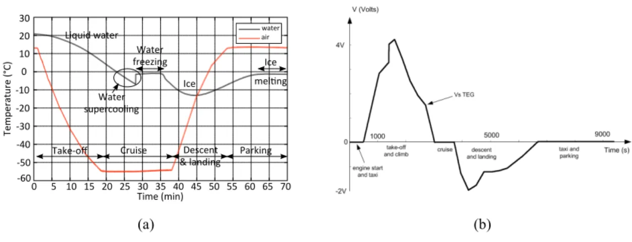
Since from take-off to cruise altitude, atmospheric temperature usually strongly decreases, thermal gradients may therefore appear inside and around the WSN node hardware. Referring to the International Standard Atmosphere (ISA) defined by the International Civil Aviation Organization (ICAO), at an en-route flight altitude of 12000 m, atmospheric temperature is about -60°C [7]. The above gradients can be converted into voltage via a thermoelectric generator (TEG) based on the Seebeck effect. However, sooner or later, the node and its surroundings will be back to an isothermal state and no more thermal flux will take place. Therefore, to both increase the gradient value and duration, we chose to capture the transient thermal gradient between aircraft mechanical structure and a phase change material [8-10]. We identified water as a pertinent choice, therefore benefiting from its high specific heat (4.2 J/g.°C – to be compared with that of Si, 0.7 J/g.°C). Water freezing point (0°C) being situated within the aircraft temperature usual operating range, the system also benefits from energy exchanges related to water latent heat of fusion (330 J/g), with the added advantage of water being maintained at a constant temperature during the water freezing or ice melting phases, hence increasing temperature gradient values. Fig. 1 shows a cross-section drawing and a photograph of the experimental setup that allowed validating the thermal-gradient energy-scavenging principle.
(a) (b)
Fig. 1. Cross-section (a) and photograph (b) of the experimental setup for the testing of the thermo electric generator: airflow is temperature-regulated and a small air volume in the capsule allows absorbing the water volume variation at phase change. View (b) shows the Thermostream® climatic chamber test head
To roughly assess the upper limit for the thermal energy that could be captured, let us consider a sealed tank containing 1 g of water. As already mentioned, water exhibits a specific heat C of around 4.2 J/g.°C when liquid, 2.1 J/g.°C when solid, and an enthalpy of fusion Hf of 330 J/g. Stating a water capsule temperature at take-off of 15°C, and a cruise temperature of –60°C, the
energy WT associated with temperature variation ΔT and phase change is given by:
WT = ΔTsolid.Csolid + ΔTliq.Cliq + Hf = 519 J/g (1)
This value may be doubled as temperature variations take place both during climb and descent that is a total of 1038 J/g. This value may be slightly higher if take-off temperature and therefore initial temperature of the sensor node is higher. Unfortunately, it can conversely be very limited if this temperature is below icing temperature.
Fig. 2 shows a typical voltage response of a TEG under transient thermal gradients created with the apparatus of Fig. 1 including 10g of water and the climatic chamber described in section IV. This figure also provides the temperature profile applied to the TEG that corresponds to a typical one-hour flight. As can be observed, gradient polarity is reversed during descent, asking for rectifying the TEG output.
(a) (b)
Fig. 2: Temperature profile (a) applied to the TEG with a climatic chamber corresponding to a typical one-hour flight at 10000m altitude – temperature is 20°C at take-off and 15°C at landing and associated TEG output voltage response (open load).
As shown in Fig. 2, thermal energy can be converted into electrical energy by thermoelectric generators using the Seebeck effect. Such generators are current sources converting temperature difference between a cold and a hot surface into electrical energy. Despite the efficiency of such components that may be as low as 1% or less, the energy available at the TEG output is around 15J. This efficiency could be even more improved using an appropriate phase change material and an optimised heat storage unit [10].
Although the above method is attractive, energy scavenging will only start once the aircraft is climbing; this may raise operational issues if energy-storage devices are initially empty. This latter situation may often occur since ultracapacitors are known to suffer from large self-discharge currents. In particular, monitoring of the structure during take-off is of great interest
water& air&
Take*off& Cruise& Descent& &&landing& Parking& Liquid&water& Ice& Ice& && mel<ng& Water&& freezing& Time&(min)& 0&&&&&&5&&&&10&&&15&&&20&&&25&&&30&&&35&&&40&&&45&&&50&&&55&&&60&&&65&&&70& T e m p e ratu re &( °C )& 30& 20& 10& &0& *10& *20& *30& *40& *50& *60& Water&& supercooling&
since it is submitted to high strains. To cope with this drawback, we devised a system with a secondary energy source harvesting the mechanical energy associated with the vibrations of the aircraft structure. In an airliner, vibrations are maximum in engine area, and conversely are much less in cabin, with the exception of low (less than 10 Hz) accelerations associated with gust or turbulence. Fig. 3 qualitatively shows the experimental vibration spectrum recorded in close proximity of the jet engine of a large airliner. It is a multi-band spectrum, made of peaks regularly spaced. The fundamental frequency corresponds to the rotating speed of the fan of the engine low-pressure compressor. Its value - and those of the harmonics - are consequently depending upon flight phase, i.e take-off, climb, cruise... Moreover, the frequency peak is only a few hertz wide. These two characteristics make energy harvesting a difficult task when using narrowband piezo harvesters.
Fig. 3: Experimental amplitude spectrum of acceleration versus frequency. Acceleration was measured by an accelerometer located in aircraft engine area during descent. Both scales are logarithmic. The fundamental frequency component ranges typically between 40 and 60 Hz depending upon flight phase and engine model
To harvest vibrations, we devised a MEMS harvester based on a seismic mass applying the vibrations to piezoelectric beams [11] [12]. It delivers an alternating output which spectrum exhibits a fundamental frequency around 60Hz, i.e. at the rotating speed of the engine inlet fan. These vibrations originating from aircraft engines are not intense enough to power all the functions of the WSN node by themselves. However, as will be shown later, they are sufficient for biasing the electronics associated with the TEG alone as soon as the engines start, therefore saving time with respect to the scavenging of thermal gradients alone.
III. ARCHITECTURE OF THE MULTISOURCE BATTERY-FREE ENERGY GENERATOR
As already mentioned, the large deployment of wireless sensors, in particular for SHM is still limited by the issue of energy autonomy of the sensor node. Energy harvesting is an attractive solution to provide battery lifetime extension or even almost infinite autonomy to a battery-free sensor node. In this context, many authors have contemplated multisource harvesting to achieve a generic power generator for wireless sensors [13] [14]. In [13], four sources (solar, vibrations, RF, thermal gradients) are combined and in [14], thermal energy harvesting is coupled to RF power to charge a microbattery. Both papers mainly focus on the validation of multiharvesting concept and its related power management. In both cases, the storage unit is placed after the voltage regulation block. Even more complex multi-source energy platforms have been theoretically envisioned in the literature
ac
ce
le
ra&
o
n
)
frequency)
fundamental*frequency*[15]. They not only deal with energy harvesting, but perform sensing and communication management from the point of view of energy transfer and storage efficiency. Despite the fact that these functions are ultimately mandatory in a wireless sensor, we have not implemented them in the more limited context of our work.
The main originality of the architecture we propose for a multisource energy generator (Fig. 4), consists in the combination of complementary energy sources for a rapid start-up of the self-powered battery-free system. It was initially motivated by aeronautics applications but is also applicable to other SHM scenarios and is compatible with other energy sources. The basic principle is to use a TEG as the primary source of energy whereas a piezoelectric generator is used as a secondary source. The latter one provides the necessary bias for the rectifier circuit required for the TEG and partially compensates the WSN node energy consumption during cruise over a long flight. The energy provided by the secondary source, through a voltage doubler with external Cin capacitor, is stored after rectification in a small capacitor Cbias that biases the voltage reference circuit (PTAT/BGR block). This circuit provides the bias current for the amplifiers in the active diodes. Once activated, these diodes allow harvesting energy from the TEG and storing it in ultracapacitors (UC1 and UC2) to be chosen with optimized leakage currents to minimize losses. To simplify circuit design, we have not considered implementing a Maximum Power Point Tracking (MPPT) procedure such as the architecture used in [16]. Consequently, depending upon ultracapacitors charge level, power captured is not permanently maximized.
Finally, voltage regulation is implemented using a low-dropout (LDO) regulator based on a PMOS power transistor. The energy generator should be able to supply a wireless sensor node. To allow an adequate use of the available energy, a careful power management of the WSN node (appropriate periodic measurement and communication, sleeping mode management) has to be implemented to save energy.
The main design challenges for the energy generator are:
Firstly, maximizing the transfer of energy from the transducer to the storage devices.
Secondly, as the voltage on the ultracapacitor storage devices will vary according to their discharge, a voltage regulation is needed. In this case, priority should be given to conversion efficiency.
For both of these design challenges, another important requirement is microscale compatibility thus prohibiting the use of bulky passive devices as the ones needed for some impedance matching strategies [17], for example.
Finally, harvested energy being limited, the quiescent power consumption of the energy generator should be as low as possible. This is required for two reasons: the first one is that many SHM scenarios are using duty cycles with much longer periods in quiescent mode than in the active one and the second is related to the self-discharge current of ultracapacitors which is in the order of µA. The quiescent current of the power converter should not be higher than this value or even be made negligible compared to it. A trade-off will then have to be made between efficiency and power consumption.
For this latter challenge, we decided for the design of each analog block of the circuit to favour solutions minimizing the number of transistors.
Fig. 4: Electrical schematic of the proposed battery-free multisource energy generator connected to a sensor node. Diode symbols (Dp1, Dp2, Dn1, Dn2, Dp3) labelled with * are active diodes (see electrical schematic in Fig. 5) and capacitor symbols (UC1 & UC2) labelled with * are ultracapacitors. PTAT/BGR block provides the bias current for the active diodes and the voltage reference for the LDO. The energy transducers are represented by their respective electrical model.
(a)
(b)
(c)
Fig. 5: Classical voltage rectification using a Graetz bridge and one ultracapacitor UC1 for storage (a). Use of two storage devices, UC1 and UC2, to maximize energy transfer (b). Optimized solution with active diodes and two storage devices (c).
A. Energy transfer maximization
As the energy harvested through thermal gradient results in two voltage polarities, even if there is only one polarity switching, a rectifier circuit is mandatory before storage. The classical solution consists in using a diode bridge such as the Graetz circuit, Fig. 5(a). The first drawback of this solution is that it does not allow maximizing the transfer of energy. For example, if the first voltage alternation is higher than the second one (it is the case in Fig.2), it will not be possible to harvest the energy from this second alternation. To cope with this problem, the solution consists in implementing two ultracapacitors for the storage as shown in Fig. 5(b): UC1 for the positive alternation and UC2 for the negative one.
The second drawback of the Graetz circuit is that two diode thresholds are lost for the rectification of each voltage alternation. To avoid this power loss, we then implemented the Graetz circuit using active diodes [17-19] as shown in Fig. 5(c). However, as shown in Fig. 6, the active diode requires a voltage reference circuit to bias the amplifier (gn and gp bias signals provided by
PTAT block in Fig. 5(c)). The design of this amplifier is critical and three important properties are required: Ultra-low power consumption to comply with our requirement of a low quiescent current of the full converter.
Threshold voltage of MOS transistors as low as possible and independent of process variations as well as layout mismatching. The main issue could be the oscillation of the driving signal provided by the operational amplifier to the gate of the MOS switch. For example, in the 0.35µm HV CMOS technology, we used isolated high-voltage (20V) MOS transistors with a typical threshold voltage of 0.5V.
High DC gain.
This latter condition, although requiring large size transistors, guarantees the second condition.
For the start-up of the active diodes, a minimum voltage around 0.9V (Vth + VDsat) is required to bias the current mirrors and
the differential pairs shown in the electrical schematics of Fig. 6. Once this voltage is reached, the threshold voltage of the active diode is given by the source to drain voltage of the MOSFET switch. Thanks to the regulation loop introduced by the operational amplifier that is designed with a high DC gain, this voltage is equal to the offset of the operational amplifier and can then be very small (few tenths of mV are targeted) compared to a classical diode threshold voltage. Nevertheless, before reaching this start-up voltage, the parasitic body diode of the MOSFET switch allows starting the rectifier with a standard diode threshold (~ 0.7V). In the case of totally discharged ultracapacitors and a single energy source (namely TEG), several minutes are needed to reach 0.9V.
Fig. 6: Symbols (top) and electrical schematic for the active diodes Dn (left) and Dp (right).
B. Energy efficiency
We optimized the design of the active diodes with the objectives to get a threshold voltage in the range of 10 mV whereas minimizing the quiescent current consumption in the range of few hundreds of nA. To generate such a low bias current (10nA/branch), we designed a nanowatt voltage and current reference [20-22]. To this purpose, we combined subthreshold MOS devices with transistors working in the linear region and did not use any resistor as shown in Fig. 7.
Fig. 7: Proposed nanowatt voltage reference.
In this circuit, all transistors are working in saturation except N1 and N2 NMOS transistors that are in weak inversion (subthreshold region) and N3R, a very long channel transistor operating in the linear region, which acts as a high-value resistor [22]. Since N1 and N2 are working in the subthreshold region, the source voltage of N1 and then the drain voltage of N3R are given by:
�
!"!= �!"!!= �!ln !!!!!!
where is �!=�� � is the thermal voltage, proportional to absolute temperature (PTAT), and SN1, SN2, SP1, SP2 are W/L ratios
of the respective MOSFET’s.
As a result, the current flowing in N3R transistor is:
� =!!! !"#!!ln !!!!!! ! !!!!! (3)
with RonN3R, the on-resistance of N3R transistor. This current is then proportional to the absolute temperature. To define a very
low reference current (~10nA), a high value resistor (~5MΩ) is needed. To reach such a value, the channel length of N3R transistor was designed as long as 330µm. It has to be noticed that, for matching reasons, N4 transistor has also the same very long channel.
The expression of the reference voltage Vref, that is equal to the gate voltage of N4, is the following:
�!"#= 2�
�!!+ �!! (4)
where �!! is the transconductance of transistor N4 and Vth its threshold voltage. Since Vth has a negative temperature
coefficient, Vref can be made independent of temperature. The value of Vref can then be adjusted through the size of the
transistors. We have chosen to define it at 0.8V. In the 0.8µm SOI CMOS technology, respective aspect ratios W/L in µm of the transistors are: 60/30 for P1, P2 and P3, 20/20 for N1 and 160/20 for N2, 6.4/330 for N3R and 3.2/330 for N4.
A very similar current source subcircuit was proposed by Ueno et al [23] to generate a nanowatt voltage reference. The main differences are the choice of using all the transistors in the subthreshold region except for the long-channel transistor, a more complex bias voltage subcircuit and the need for a start-up circuit. Compared to our proposed voltage reference, it has better performance regarding temperature sensitivity (15 ppm/°C vs 290 ppm/°C) and line sensitivity (20 ppm/V vs 800 ppm/V). Nevertheless, the reduced number of transistors of our proposed voltage reference allows a very low quiescent power consumption of 600 nW with a 3V power supply for the whole multisource converter to be compared to the 300 nW at 1.5V for the single voltage reference circuit.
(a) (b)
Fig. 8: Comparative simulation of the generated voltage Vbias across the storage device Cbias during a one-hour flight. (a) Simulation set-up shown for the case of the combined energy sources, Pz input being grounded when only the TEG source is used. The energy sources are simulated using their equivalent electrical model and a voltage input corresponding to the output of the respective transducer under typical flight conditions. (b) Simulation plot of Vbias voltage across
Cbias capacitor when using only a TEG for energy generation (“Vbias without piezo”) and the combination of a TEG with a piezoelectric transducer (“Vbias with piezo”). Also plotted is the TEG output voltage, Vs TEG, used for the simulation. Voltage output of the piezoelectric transducer, Vpz, is an AC voltage with
±3V amplitude and 60Hz frequency.
In addition, to limit the effects of process mismatches, particular care was taken for the layout and routing of the amplifier and voltage reference circuit (use of dummy devices, common centroid patterns...). Moreover, the very long channel transistors, N3R and N4, are designed in an isolated well including guard rings and good well contacts to insure a constant biasing of the substrate along the long channel.
As mentioned earlier, the originality of the proposed energy generator circuit is the combination of the TEG with a piezoelectric transducer to provide a rapid start-up of the energy scavenging from the TEG and a complementary source of energy during cruise. This beneficial effect is demonstrated on the simulation results of Fig. 8 that compares the case of the energy generation using the TEG alone with the TEG combined with the piezoelectric transducer. It can be noticed that using a multisource approach, the energy generator is operational as soon as the engines start.
Another important parameter that allows maximizing the energy transfer is the value of the storage ultracapacitor (UC). The time required to charge an UC depends on the time constant RS.UC of the circuit. This is particularly relevant since the energy
generation is only transient during take-off and descent. If the value of the UC is too small, it will be rapidly charged but its maximum operating voltage, together with its small value, will limit the stored energy. On the contrary, if its value is too large, the time constant will prevent collecting the maximum of energy since the UC will not have the time to reach the voltage saturation. To optimize this trade-off, we simulated the charge of an UC via an ideal diode during the aircraft take-off and compared the open-circuit voltage to the one of a matched load. In our case, given the fact we use two UCs in series, the optimized value of each one is 1F [20].
Vpz$$ (±3V,$60Hz)$ $$$$$$$ Rout=$10MΩ" Vs$TEG$ Mul$source** harvester* Vout$ TEG+$ Vst9$ Vst+$ Vpol$ GND$ Vref$ Pz$ Pz$ UC1=1F$ UC2=1F$ Cbias=$ 10µF$ Rpz=$300Ω" RTEG=$300Ω" Cin=10µF$ 6 5 4 3 2 1 0 -1 V o lta g e Vbias Vbias with piezo Vbias without piezo Vs TEG engine start and taxi take-off and climb
cruise descent and
landing
taxi and parking
Time (103s)
It has to be noticed here that the piezoelectric transducer can also directly provide energy to the output, the active diode Dp3 providing isolation from the UCs since the piezoelectric transducer would not be able to directly charge them given the very small current (~µA) generated by mechanical vibrations in the aeronautics environment. However, this direct connection to the output VOUT could be very useful to provide energy to the WSN node either on ground, as soon as aircraft engines start, or during
long flights (several hours) since in these cases, the TEG might be inactive.
Fig. 9: Electrical schematic of the LDO with the proposed voltage reference circuit and the capability of generating two regulated output voltages, Vref or 2Vref, according to the command on transistor P6.
Finally, a voltage regulation stage is required after the UC. Ideally, it should exhibit high conversion efficiency. The best candidate would be a switching regulator. However, given its complexity, in terms of quiescent power consumption, it will be less efficient than a simple linear regulator. We then chose to implement a low-dropout regulator (LDO) using a PMOS power transistor because of its simpler driving (no charge pump needed). The proposed nanowatt bandgap reference (BGR) circuit based on MOS devices allows providing the voltage reference for the LDO that is designed to supply a maximum peak current of 20mA.
The proposed energy generator provides two regulated voltage values: Vref or 2Vref that can be switched using an external command (Fig. 9). It has to be mentioned that in this circuit, N3R, N4 and N6 transistors have both a very long-channel and can be designed in the same isolated well.
Regulated voltages are required for supplying signal processing and memory circuits. For less sensitive circuits, a direct power supply from the UCs could be implemented. This would have the advantage to greatly increase the global efficiency.
IV. EXPERIMENTAL RESULTS
This multisource and battery-free energy harvesting architecture was validated on two technologies: a high-voltage 0.35µm CMOS technology from AMS available via the French Multi-Project Chip (CMP) service and a smart power 0.8µm Bipolar CMOS DMOS merged technology on SOI (TFSMART1) provided by Telefunken Semiconductors [24]. Optical views of these test chips are given in Fig. 10. On the first test chip (0.35µm CMOS), we validated the nanowatt voltage reference and the global
architecture with a single source, i.e. the thermogenerator. On the second one (0.8µm SOI), we validated the multisource architecture. Both technologies provide high-voltage devices. A high-voltage technology is required since both the chosen thermoelectric generator, a Micropelt GmBH (MPG-D751), and the laboratory-made piezoelectric generator [11] [12] could generate voltages as high as 10V. Both technologies allow isolating the active diodes and the very long channel transistor. The SOI technology has the additional advantage to completely eliminate any parasitic structure that could be triggered on in severe environment.
Fig. 10: Optical views of the two test chips: 0.35µm High-voltage CMOS (left) and 0.8µm smart power SOI (right).
A. 0.35µm CMOS testchip
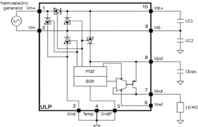
In this technology, several types of transistors are available. For the needs of this circuit, we chose transistors with the lowest threshold voltage and with an annular layout to limit leakage current and improve radiation immunity. Two versions of the circuit were designed on the same die: an ultra low-power (ULP) with 10nA/branch and a low-power (LP) with 100nA/branch. The total size of the chip is 1.7mmx1.7mm.
Both LP and ULP versions of the circuit are functional. We only report here the results for the ULP circuit. Fig. 11 describes the block diagram of the ULP circuit. In addition to the functional pins, a dedicated pin called Temp allows sensing the silicon die temperature via a diode. Vbgr pin allows checking the functionality of the bandgap reference circuit as well as implementing an output voltage of 0.8V by short-circuiting it to Vout pin. Vin+ and Vin- are the pins for the connection of the thermogenerator (TEG). Vpol is the pin for the connection of the small capacitor Cbias that has a value of 10µF. This capacitor allows the self-biasing of the circuit. Three pins are implemented for the ground rails: two for the internal circuit and one for power (GndP). Vst+ and Vst- are the pins for the connections of the two ultracapacitors, UC1 and UC2 whose value is 0.9F.
Fig. 4: Electrical schematic of the ultra low-power (ULP) circuit with the external elements needed for the energy generation.
As already mentioned, the circuit allows providing two values for the regulated voltage Vout, which can be chosen by externally connecting the pins Vout and Vbgr. The targeted values were 1.6V and 0.8V, respectively. This could also be implemented via a specific internal circuitry triggered by an external logic signal.
For the targeted application of AHM that requires a high-energy autonomy, it is very important to choose an ultracapacitor with the best long-term self-discharge properties. These properties depend on the way the ultracapacitor was previously charged. Among commercially available devices, Maxwell HC series, after being charged with a constant 5mA current, presents a self-discharge of only a few % after 12h that is fully compatible with our application. This self-self-discharge is even smaller if the charge current is lower than this value, which will be mainly the case for energy harvesting applications. In the same way, the storage capacitor Cbias (10µF) also needs the same property of low leakage current to guarantee a good efficiency of the energy generator.
For the functionality testing, the energy generator is emulated using an electrical-waveform generator. First of all, we checked the functionality of the active diodes. As shown in Fig. 12, both diode types provide a very low diode threshold around 20mV, as expected from the simulations.
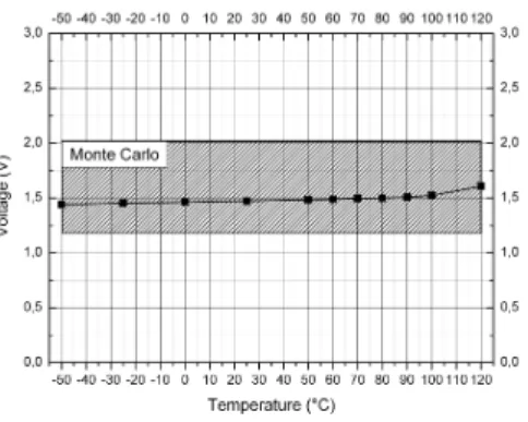
We also measured the values of the regulated voltage and of the quiescent current and their dispersion over the 10 dies received from the CMP service. As shown in Fig. 13, the measured values perfectly fall within the range defined by Monte-Carlo simulations. 1! 2! 3! 4! 5! 6! 7! 8! 9! 10! Vref!
Fig. 12: Experimental characterization of the active diodes.
We also checked the temperature behaviour of the circuit. The temperature specifications of the application covers a wide range from -50°C to 100°C. As can be seen from Fig. 13, the temperature performance is a variation of 290 ppm/°C that is sufficient for the application and quite good for a PTAT/BGR block only consuming 100nA and without any offset compensation circuitry.
Fig. 13: Temperature behaviour of the regulated output voltage compared to the range defined by Monte Carlo simulations.
For the validation of the energy generation from transient gradients, we were not able to perform in-flight testing. However, our partner, Airbus, provided typical temperature profiles that we used in our experimental test bench.
To simulate the aircraft temperature conditions, we tested the TEG scavenging module of Fig. 1 into an environmental test system TP04200A ThermoStream® from Temptronic corporation. To model the evolution of the temperature during a flight, we chose the standard atmosphere model of ICAO, that is a temperature of 15°C (59°F) and a pressure of 1013.25 hPa (14.7 psi) at sea level, and a decreasing rate of -6.5°C/km until the limit temperature -56.5°C.
Fig. 14 presents the results of measurements simulating a one-hour flight using the TEG for energy generation without drawing any current. As expected, since transient gradients build up at take-off, the circuit is only active after a few minutes (~10 min). The total energy that is collected during such a flight is equal to 4J. Compared to the original harvested energy of 15J obtained on a matched load, the losses are mainly due to the impedance mismatching and to the late triggering of the active diodes. The observed slight decrease of Vout voltage during cruise and on ground is related to the intrinsic leakage currents of
the various devices in the system (UC1, UC2, Cbias and quiescent current of the integrated chip).
Fig. 14: Energy generation with thermal gradient using a Micropelt MPG-D751 device: simulation of a one-hour flight. This test is performed without drawing current.
Fig. 15: Energy generation with thermal gradient using a Micropelt MPG-D751 device: simulation of a one-hour flight. A continuous current of 220µA is drawn during this test.
To validate that the captured energy would allow supplying a wireless sensor node, we performed the same experiment with a continuous current consumption of 220µA. It can be observed from Fig. 15 that sufficient energy is stored into the ultracapacitors to provide a regulated voltage over the whole flight, until t=8000s well beyond landing. This means that with appropriate power management, for example, periodic measurement and communication that would greatly reduce the power consumption, the same amount of energy should allow supplying the WSN node over a longer flight.
B. 0.8µm Smart Power SOI testchip
In this technology, we implemented the full battery-free multisource energy generator as shown in Fig.16. Active diodes are also implemented in the voltage doubler used for the rectification of the signal originating from the piezoelectric transducer. The
value of the external input capacitance of the voltage doubler, Cin, is 10µF. This testchip, shown in Fig. 10, was designed with a
regulated output voltage value Vout of 2.4V.
Fig. 16: Electrical schematic of the multisource and battery-free energy generator.
The circuit was tested under the same conditions as the previous test chip. Firstly, we validated its functionality using one single energy source, the thermogeneration, using the thermal profile simulating a one-hour flight. The measurement data are presented in Fig.17 that shows a voltage regulation at 2.45V operational at a time of 650s.
Fig. 17: Energy generation from thermal gradients using a Micropelt MPG-D751 device (_TEG) and from two sources, thermal gradients and vibrations (_TEG+PZ): experimental simulation of a one-hour flight. Vst_x is the voltage stored on the ultracapacitors and Vout_x is the output regulated voltage.
To simulate the multisource energy generation, we replaced the piezoelectric transducer by its equivalent impedance (300Ω) and applied an oscillating waveform with 60Hz frequency and 3V peak amplitude using a voltage generator. These parameters were defined in order to correspond to the experimental data of Fig. 3 in terms of frequency, and to a high level of vibrations (aircraft engines area and climb phase). As shown in Fig. 17, the regulated voltage is available much earlier (400s). However, this setup time is much higher than the one expected from the simulated one (a few seconds in Fig.8). We analysed the reasons for this big discrepancy and found out that the ESD protection network, involving Zener diodes with a threshold of 6V, is
1! 2! 3! 4! 6! 7! 8! 9! 10! 11! 5! Vref! 0,0# 1,0# 2,0# 3,0# 4,0# 0# 1000# 2000# 3000# 4000# 5000# Vo lt a ge#( V) # Time#(s)# Vout_TEG_&_PZ# Vst_TEG_&_PZ# Vout_TEG# Vst_TEG# Vst_TEG(+(PZ( Vst_TEG( Vout_TEG(+(PZ( Vout_TEG(
unexpectedly triggered on and is deriving an important part of the energy generated by the piezoelectric transducer, thus considerably degrading the efficiency of the voltage doubler. To cope with this issue, the solution we contemplate consists in using a rectifier stage that is self-protected with regards to ESD without the addition of any protection devices. Despite this loss, the earlier start-up of the active diodes allows greatly improving the energy transfer to the ultracapacitors: up to 32% compared to the single TEG source. As a result the total energy collected is now 10J that corresponds to a power harvester efficiency, defined by (effective power on storage)/(harvester raw power on matched load), of 66%. The static efficiency of the standalone converter (without the ultracapacitors but with the small Cbias capacitor) was measured in two configurations (Fig. 18): by applying a DC power supply (3V or 4V) either to Vpol, (TEG and PIEZO source inputs being grounded) or directly to both TEG (Vin+/-) and PIEZO (Pz+/-) source inputs. The converter efficiency is computed by the ratio between the output and input powers measured using Agilent N6705B DC Power Analyzer. The remarkable result is that the active diode stages do not impact the global converter efficiency that is mainly defined by the LDO one.
Fig. 18: Measured static converter efficiency using Agilent N6705B DC Power Analyzer for different output powers: comparison between setting the power supply, 3V or 4V, at the LDO source (ηLDO) and at the TEG/PIEZO inputs (η).
When the output voltage is stabilized, the quiescent current of this circuit is 300 nA for a DC power supply of 3.5V. Regarding the active diodes, they exhibited an average threshold of 26 mV. We also tested the circuit behaviour over temperature and obtained a regulated output voltage with a variation of 271 ppm/°C very similar to the one achieved with the 0.35µm CMOS technology.
Recently, several commercial solutions were proposed for a similar energy generation function. We compare in Table 1 the performance of the proposed converter to the solution proposed by Linear Technology with the LTC3105 [25] and to the energy harvesting evaluation unit, TE-Power PLUS, proposed by Micropelt [26]. The results of research works [10] [13] [14] [27] are also given for reference. Although the different converters are difficult to compare in terms of complexity and performance, the quiescent current of the proposed converter is well below the value of both commercial and academic circuits. One of the circuits, namely the one from the Imperial College [10], has a very similar application is but only uses a thermogenerator for power harvesting. In terms of efficiency, at Vin=3V, despite the use of an LDO regulator, the converter we propose has a better
0" 10" 20" 30" 40" 50" 60" 70" 80" 90" 100" 0" 5" 10" 15" 20" 25" 30" E ffic ie n cy (( %) ( Pout((mW)( Power(supply(on(Piezo(&(TEG(vs(LDO(source(( η(@3V( ηLDO(@3V( η(@4V( ηLDO(@4V(
efficiency and compares quite honestly to the other circuits that use switched-mode DC/DC conversion. LTC3105 TE-PowerPlus [10] [13] [27] [14] Proposed converter Quiescent
current 10µA 3.2µA NA 27µA 70µA 300nA
Maximum efficiency Pout/Pin 90% ≥ 70% NA 75-85% 50% 82% Harvested energy efficiency NA NA 60% 70% NA 66% Regulated voltage (LDO) 2.2V 2.4V 3.3V 1.2V 2.5V 2.4V
Table 1: Comparison of the performance of the proposed converter to commercial solutions LTC3105 from Linear Technology and TE-Power PLUS from Micropelt and to the results of research works [10] [13] [14] [27].
V. CONCLUSION
The multi-source energy generator presented in this paper exhibits two advantages compared to available commercial solutions. First, it allows using two sources of energy, which is a significant advantage for the concept of energy harvesting since the availability of a single energy source in a given environment is not guaranteed. The second advantage is its ultra-low power consumption that is critical for the autonomy of a battery-free wireless sensor node.
This circuit was designed for a specific SHM aeronautics application where transient gradients and permanent mechanical vibrations are used as energy sources. Vibrations provide a secondary source mainly used to self-bias the circuit, which does not include any battery and stores energy into ultracapacitors. The proposed circuit, realized in a 0.35µm CMOS technology, exhibits 200nA quiescent current and 300nA in the 0.8µm Smart power SOI technology well below values of commercial products. This system was also validated on a test bench emulated with realistic mission profiles. Finally, the innovative building blocks presented in this paper may find applications in field outside aeronautics.
REFERENCES
[1] B. Mitchell, “Energy Harvesting Applications and Architectures at Boeing Commercial Airplanes,” presented at NanoPower Forum, San Jose, CA, 2007. [2] L. G. dos Santos, “EMBRAER Perspective on SHM Introduction into Commercial Aviation Programs, ” in Proc. 8th International Workshop on Structural
Health Monitoring (IWSHM), Stanford, CA, 2011, vol.11, pp. 19-26.
[3] Ultra Electronics Aircraft systems: http://www.ultra-electronics.com/aircraft_systems/airframe_fatigue.php
[4] D. Meekhun, V. Boitier, J.M. Dilhac, “Design of a solar harvester system for a wireless sensor network deployed for large aircraft in-flight tests,”
Renewable Energy & Power Quality Journal, Paper no. 856, no. 6, Avril 2012.
[5] R. Montheard, S. Carbonne, M. Bafleur, V. Boitier, J.M. Dilhac, X. Dollat, N. Nolhier, E. Piot, C. Airiau, “Proof of concept of energy harvesting from aero acoustic noise,” in Proc. PowerMEMS 2012, Atlanta, USA, pp.267-270.
[6] D. Meekhun, V. Boitier, J.M. Dilhac, “Charge and Discharge performance of Secondary Batteries according to Extreme Environment Temperatures,” in Proc. 35th Annual Conference of the IEEE Industrial Electronics Society (IECON 2009), Porto, Portugal, Nov. 2009, pp.271-275.
[7] ISO 2533:1975 Standard Atmosphere, ISO/TC20/SC6, 2013-03-20, http://www.iso.org
[8] N. Bailly, J-M. Dilhac, C. Escriba, C. Vanhecke, N. Mauran, M. Bafleur, “Energy Scavenging based on Transient Thermal Gradients: Application to Structural Health Monitoring of Aircrafts,” in Proc. PowerMEMS 2008, Sendai, Japan, Nov. 2008, pp.205-208.
[9] D. Samson, M. Kluge, T. Becker, U. Schmid, “Energy Harvesting for Autonomous Wireless Sensor Nodes in Aircraft,” in Proc. Eurosensors XXIV, Linz, Austria, Sept., 2010, pp.1160-1163.
[10] M. E. Kiziroglou, S. W. Wright, T. T. Toh, T. Becker, P. D. Mitcheson and E. M. Yeatman, “Heat storage power supply for wireless aircraft sensors, ” in
Proc. PowerMEMS 2012, Atlanta, USA, Dec. 2012, pp.472-475.
[11] H. Durou, G.A. Ardila Rodriguez, A. Ramond, X. Dollat, C. Rossi, D. Estève, “Micromachined bulk PZT piezoelectric vibration harvester to improve effectiveness over low amplitude and low frequency vibrations, ” in Proc. PowerMEMS 2010, Louvain, Belgium, Nov. Dec. 2010, pp.27-30.
[12] H. Durou, “Vers l'autonomie énergétique des réseaux de capteurs embarqués : conception et intégration d'un générateur piézoélectrique et d'un micro dispositif de stockage capacitif en technologie silicium, ” Ph.D. thesis, Université Paul Sabatier, Toulouse, France, Dec. 2010.
[13] J. Colomer-Farrarons, P. Miribel-Català, A. Saiz-Vela, and J. Samitier, “A Multiharvested Self-Powered System in a Low-Voltage Low-Power Technology,” IEEE Trans. Ind. Electron., vol. 58, no. 9, pp. 4250-4263, Sept. 2011.
[14] H. Lhermet, C. Condemine, M. Plissonnier, R. Salot, P. Audebert, and M. Rosset, “Efficient Power Management Circuit: From Thermal Energy Harvesting to Above-IC Microbattery Energy Storage,” IEEE J. of Solid-State Circuits, vol. 43, no. 1, pp. 246–255, Jan. 2008
[15] E. Beigné, C. Condemine, N. Leblond, P. Vivet, G. Waltisperger, J. Willemin, “Bringing robustness and power efficiency to autonomous energy harvesting microsystems, ” IEEE Design & Test of Computers, Vol.28, no.5, pp.84-94, Sept. Oct. 2011.
[16] E. Lefeuvre, D. Audigier, C. Richard, and D. Guyomar, “Buck-Boost Converter for Sensorless Power Optimization of Piezoelectric Energy Harvester, ”
IEEE Transactions on Power Electronics, vol. 22, no. 5, pp 2018-2025, Sept. 2007.
[17] Gyorgy D. Szarka, Bernard H. Stark, and Stephen G. Burrow, “Review of Power Conditioning for Kinetic Energy Harvesting Systems, ” IEEE Trans.
Power Electron., vol. 27, no. 2, pp. 803-815, Feb. 2012.
[18] E. Dallago, D. Miatton, G. Venchi, V. Bottarel, G. Frattini, G. Ricotti and M. Schipani, “Comparison of Two Autonomous AC-DC Converters for Piezoelectric Energy Scavenging Systems,” IFIP Advances in Information and Communication Technology, vol. 313, pp. 61-80, 2010.
[19] Yang Sun, Nguyen Huy Hieu, Chang-Jin Jeong, and Sang-Gug Lee, “An Integrated High-Performance Active Rectifier for Piezoelectric Vibration Energy Harvesting Systems, ” IEEE Trans. Power Electron., vol. 27, no. 2, pp. 623-627, Feb. 2012.
[20] C. Vanhecke, L. Assouère, M. Bafleur, C. Rossi, J.M. Dilhac, “Convertisseur à faible consommation pour la récupération d’énergie ambiante combinant
deux sources pour application aéronautique,” in Proc. 8ème Journées d’étude Faible Tension Faible Consommation (FTFC 2009), Neuchâtel, Switzerland,
2009.
[21] C. Rossi, P. Aguirre, “Ultra-low Power CMOS Cells for Temperature Sensors”, in Proc. 18th Symposium on Integrated Circuits and Systems Design,
Florianopolis, Brazil, 2005, pp. 202 – 206.
[22] C. Vanhecke, “Current generator, notably for current of the order of nano-amperes, and voltage regulator using such a generator”, US Patent n°20120068684 A1, March 2012.
[23] K. Ueno, T. Hirose, T. Asai, Y. Amemiya, “A 300 nW, 15 ppm/ C, 20 ppm/V CMOS Voltage Reference Circuit Consisting of Subthreshold MOSFETs,”
IEEE J. of Solid-State Circuits, vol. 44, no. 7, pp. 2047–2054, Jul. 2009.
[24] “SMARTIS 1, Design Manuel, Release: SIS1_0.32_071005, Atmel Germany Gmhb, October 7 2005.” [Online]. Available: http://www.telefukensemi.com.
[26] http://www.micropelt.com/down/datasheet_te_power_plus.pdf
[27] J. Colomer Farrarons, P.L. Miribel-Catala, A CMOS Self-Powered Front-End Architecture for Subcutaneous Event-Detector Devices: