HAL Id: hal-01657426
https://hal.archives-ouvertes.fr/hal-01657426
Submitted on 7 Dec 2017HAL is a multi-disciplinary open access
archive for the deposit and dissemination of sci-entific research documents, whether they are pub-lished or not. The documents may come from teaching and research institutions in France or abroad, or from public or private research centers.
L’archive ouverte pluridisciplinaire HAL, est destinée au dépôt et à la diffusion de documents scientifiques de niveau recherche, publiés ou non, émanant des établissements d’enseignement et de recherche français ou étrangers, des laboratoires publics ou privés.
Anisotropic propagation imaging of elastic waves in
oriented columnar thin films
E Coffy, Guillaume Dodane, Sébastien Euphrasie, A. Mosset, Pascal Vairac,
N. Martin, H. Baida, Jean-Michel Rampnoux, Stefan Dilhaire
To cite this version:
E Coffy, Guillaume Dodane, Sébastien Euphrasie, A. Mosset, Pascal Vairac, et al.. Anisotropic propa-gation imaging of elastic waves in oriented columnar thin films. Journal of Physics D: Applied Physics, IOP Publishing, 2017, 50 (48), pp.484005. �10.1088/1361-6463/aa92ad�. �hal-01657426�
1. Introduction
For the last few decades, numerous works have been focused on the wave propagation in anisotropic media [1–3]. This sign of interest is mainly assigned to the exciting range of prop-erties, which can be reached by only changing the probing direction in the material. Among the solid materials, assess-ment of aniso tropy can be significantly evidenced in metals since all metallic crystals are intrinsically anisotropic due to the directional differences in inter-atomic stiffness bonds in the crystal structure [4]. However, in many typically prepared
metals, the material is formed from randomly oriented crys-tals, which is conventionally defined as a polycrystalline structure. Consequently, these individual crystals are ran-domly oriented, leading to physical behaviors at the macro-scopic scale which are non-dependent on the direction.
In the case of thin film materials, the anisotropic proper-ties may become significant since these nearly-2D systems can adopt various designs, texture patterns and architectures depending on the fabrication method [5–7], particularly for metallic, semiconducting or dielectric thin films prepared by the glancing angle deposition (GLAD) method [8–10]. Due to
Anisotropic propagation imaging of elastic
waves in oriented columnar thin films
E Coffy1 , G Dodane1, S Euphrasie1, A Mosset1, P Vairac1, N Martin1 ,
H Baida1,2, J M Rampnoux2 and S Dilhaire2
1 Institut FEMTO-ST, UMR 6174, CNRS, ENSMM, Université Bourgogne Franche-Comté, 15B, Avenue des Montboucons, 25030 Besancon Cedex, France
2 Laboratoire Ondes et Matière d’Aquitaine—LOMA, UMR 5798 CNRS, Université de Bordeaux, 351, Cours de la libération, 33400 Talence Cedex, France
E-mail: sebastien.euphrasie@femto-st.fr
Abstract
We report on the observation of strongly anisotropic surface acoustic wave propagation on nanostructured thin films. Two kinds of tungsten samples were prepared by sputtering on a silicon substrate: a conventional thin film with columns normal to the substrate surface, and an oriented columnar architecture using the glancing angle deposition (GLAD) process. Pseudo-Rayleigh waves (PRWs) were imaged as a function of time in x and y directions for both films thanks to a femtosecond heterodyne pump-probe setup. A strong anisotropic propagation as well as a high velocity reduction of the PRWs were exhibited for the GLAD sample. For the wavevector k/2π = 3 × 10⁵ m−1 the measured group velocities v
x and vy equal 2220 m s−1
for the sample prepared with conventional sputtering, whereas a strong anisotropy appears (vx = 1600 m s−1 and vy = 870 m s−1) for the sample prepared with the GLAD process.
Using the finite element method, the anisotropy is related to the structural anisotropy of the thin film’s architecture. The drop of PRWs group velocities is mainly assigned to the porous microstructure, especially favored by atomic shadowing effects which appear during the growth of the inclined columns. Such GLAD thin films constitute a new tool for the control of the propagation of surface elastic waves and for the design of new devices with useful properties.
Keywords: glancing angle deposition, columnar films, acoustics, pump-probe setup, anisotropy
the anisotropic microstructure of the inclined columnar archi-tecture typically produced by the oriented growth, many phys-ical properties of GLAD films such as optphys-ical indices [11], electrical conductivity [12], wetting [13], friction coefficient [14] and so on, have shown in-plane anisotropic behaviors when they are probed in the growing direction or perpend-icularly to the columns. Such anisotropy of the film proper-ties is mainly related to the progressive broadening of the columns in the orthogonal direction to the deposition plane. By favoring an oriented growth of columnar architectures, this GLAD method also represents an original strategy and an attractive ability to produce and engineer surface behaviors in a one-step deposition process.
In this paper, we report on the surface acoustic wave propa-gation measured with a femtosecond heterodyne pump-probe setup in tungsten (W) thin films sputter-deposited on (1 0 0) silicon wafer by conventional sputtering and GLAD process. The influence of an inclined columnar architecture on the propagation of elastic waves in tungsten films compared to a classical structure (columns, which are normal to the sub-strate surface) motivates this work. Simulations with simpli-fied models based on periodic structures are presented. The correlation between the anisotropic acoustic wave velocity and the films’ microstructure is demonstrated.
2. Materials and methods
Tungsten films were deposited on a (1 0 0) Si wafer by DC mag-netron sputtering from a metallic target (51 mm diameter and 99.9 at.% purity) inside a home-made vacuum chamber. The experimental device was a 40 l sputtering chamber pumped down via turbo-molecular pump backed by a primary pump, allowing a residual vacuum of about 10−6 Pa. The tungsten target was sputtered with an argon flow rate of 2.3 cm3 min−1 and a constant pumping speed of 13 Ls−1, which produced an argon sputtering pressure of 3.0 × 10⁻¹ Pa. The target current was fixed at 100 mA and the deposition time was adjusted, so as to get a film thickness of 300 nm. No external heating was applied during the growth stage and depositions were car-ried out at room temperature. The GLAD technique [15] was implemented, in order to produce normal and tilted columnar architectures. It consists of depositing thin films under con-ditions of obliquely incident flux of the sputtered particles and on a fixed or mobile substrate. In this study, two incident angles were used: α = 0° (conventional sputtering) and 80° (GLAD technique). Scanning electron microscopy (SEM) was used to view the surface and the fractured cross-section of the films with a JEOL JSM 7800 field emission SEM.
Measurements of the acoustic waves propagation are per-formed with a femtosecond pump-probe setup [16, 17]. The acoustic generation into the tungsten film is done by the optical absorption of one femtosecond laser beam, namely the ‘pump’. Consequently, a fast temperature increase appears inducing acoustic waves via thermoelastic effect [18]. The surface reflectivity change contains the acoustic and thermal contributions. These reflectivity changes are probed by a second laser beam, namely the ‘probe’. In order to acquire the
temporal reflectance response of the film, two femtosecond lasers are used in our setup with a heterodyne configuration aka asynchronous optical sampling. The lasers are electroni-cally synchronized with a controlled frequency shift in their repetition rates (48 MHz and 48 MHz + 700 Hz). This gives rise to an additional time difference between the pump and the probe of about 300 fs for each pump excitation (every 20.8 ns). Compared to traditional pump-probe setups using a mechan-ical delay line, this technique removes the mechanmechan-ical vibra-tions and the variavibra-tions in size of the focal spot due to a slight divergence/convergence of the optical beam. It also allows a whole time spanning of 21 ns with a resolution of about 1 ps. At the output of the lasers, the duration of the pulses is 180 fs. The central wavelength of the beams is 515 nm (frequency doubled Yb:YAG lasers). The two beams are focused on the sample surface and the resulting radii (1/e2) of the spots’ size is around 1 µm. For a map of the acoustic signal at the sur-face of the film, the pump spot is scanned by means of a lens set controlled with a 2D translation stage in the pump optical path. The scan of the pump spot is performed over an area of 50 × 50 µm2.
Numerical simulations of the surface acoustic wave propa-gation are performed with the finite element method. The physical parameters as mass densities and elastic constants of silicon and tungsten are given in table 1, keeping in mind that elastic constants may differ from the bulk material, especially for thin films [19]. Unit cells are described and explained in part 3. Bloch–Floquet periodic conditions are applied on boundaries external to the unit cell, both in x and y directions according to equation (1): uj →P + al→rl = exp(ikjal)· uj →P (1) where uj is the displacement in the x, y or z direction, vector P
represents the position, al is the period, vector rj is the unitary
vector and kj the wavevector in the x or y direction depending
on the boundary. The x and y directions correspond to the crys-tallographic axes. These structures are therefore simulated to be infinitely periodic in both directions. Bottom boundaries of the models are mechanically set as fixed. Dispersion curves are obtained by varying the wavevector k in the range of interest in the two directions.
3. Experimental results
SEM observations of as-deposited tungsten thin films pro-duced by conventional sputtering (α = 0°) exhibit a dense and polycrystalline (x-ray diffraction not shown here) columnar microstructure, which is perpendicular to the substrate surface (figures 1(a) and (b)). This morphology is typical of sputtered metallic films and corresponds to the first zone of classical structural zone models [20, 21]. A fine fiber texture develops
Table 1. Properties of silicon and tungsten used for calculations. Material ρ (kg m−3) c
11 (GPa) c12 (GPa) c44 (GPa)
Silicon (Si) 2330 166 63.9 79.6
in pure elemental films sputter-deposited at room temper-ature. Due to the high melting point Tm of tungsten (3695 K at 1 atm) and no external heating during deposition (the sub-strate temper ature Ts increases a few degrees at the end of the growth), the temperature Ts/Tm ratio is lower than 0.1, which corresponds to the first zone of the structural zone models. This kind of film typically exhibits density close to 95% of the bulk material and isotropic behaviors.
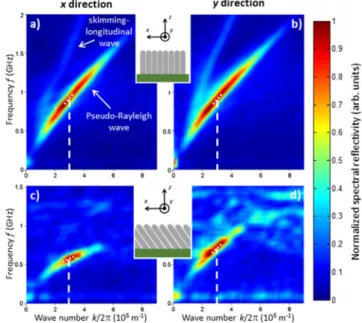
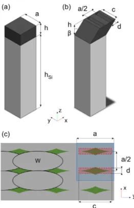
For tungsten films prepared by the GLAD process with an incident angle α = 80°, a well-defined and inclined polycrys-talline columnar microstructure is clearly viewed from the cross-section SEM observation (figure 1(b)) with a column angle β = 43°. This difference between α and β angles is commonly met in GLAD films, and is also assigned to the shadowing effect and diffusion of the particles on the growing film. Similarly, the surface observation shows a voided and corrugated surface (figure 1(b)). From this top view, one can see asymmetric and elongated holes between columns. Such columns also show an elongated shape with a long axis, which is perpendicular to the direction of the incoming particle flux (white arrow). These anisotropic structural characteristics have already been reported by Tait et al [22]. They are mainly connected to the geometric shadowing effect and a favored diffusion of the incoming sputtered atoms in the direction
perpend icular to the incidence of the particle flux. This atyp-ical growth, specific to oblique angle deposition, leads to elliptical columns with their long axes perpendicular to the plane of incidence. Increasing the film’s thickness produces chains of columns [23], which are transverse to the particle flux direction, as illustrated in figure 1(b). As a result, the column is able to grow along the y direction, which leads to a progressive fanning of the column cross-section. With such a fanning of the individual columns, the lateral growth allows neighboring columns to be in contact and chain together. This gives rise to a preferential bundling of the columnar microstructure following the y direction. Chaining and fan-ning phenomena produce elliptical shapes of the columnar cross-section and thus, a significant structural anisotropy is developed. The latter generates a corresponding anisotropy in the acoustic wave propagation, as shown in figure 2. The wave amplitude obtained from the pump-probe measurements is chronologically illustrated after 200 ps and until 6 ns for conventional films (α = 0°) and those prepared by GLAD (α = 80°). It is worth noticing the circular and concentric rings observed for conventional films (anisotropy of silicon has a very weak influence), whereas elliptical shapes are clearly viewed for inclined columnar structures. The aniso-tropic propagation is thus evidenced and intimately connected to the microstructural anisotropy of tungsten films produced by the GLAD process.
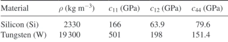
Figure 3 shows the relative variation of the reflectivity (ΔR/R) as a function of time, along the x direction for the tungsten films with sputter-deposition (α = 0°). The thermal background has been subtracted; the ΔR/R color bar scale gives the level of the acoustic part of the signal. Two different wave packets are observed. The integral of the squared relative reflectivity over the time was calculated for each wave packet. It gives information about how the elastic energy decreases as the wave propagates. For the slowest wave, it is found to decrease proportionally to the inverse of the distance. This is typical of a surface wave and, considering the symmetry of the source, this wave is a pseudo-Rayleigh wave. On the other hand, for the fastest wave, it is inversely proportional to the square of the distance, indicating this wave to be the skim-ming longitudinal one (surface part of the volume longitudinal wave). The pseudo-Rayleigh wave is very dispersive (velocity strongly frequency dependent). Similar measurements have been performed for the x and y directions for tungsten films prepared by the GLAD technique using α = 80° (not shown here).
The dispersion curves (figure 4) have been obtained by plotting the FFT-2D (2 dimensions discrete Fourier transform) of the relative reflectivity versus time and position as typically shown in figure 3. The local slope of these dispersion curves directly corresponds to the group velocities. The short laser pump pulses excite waves with frequencies in the GHz range and with wavelengths of a few micrometers. The dispersive behavior of the pseudo-Rayleigh waves is also observed in figure 4 since the frequency versus wave number plots do not exhibit a linear behavior. For tungsten films prepared by conventional sputtering (α = 0°), dispersion curves are very similar following x and y directions (figures 4(a) and (b)) Figure 1. Schematic views with cross-section and surface SEM
observations of as-deposited tungsten thin films 300 nm thick sputter-deposited by (a) conventional dc magnetron sputtering and (b) GLAD process. An incident angle α = 80° of the particle flux was used for GLAD films. Arrows indicate the incoming flux of tungsten atoms, which leads to an inclined columnar architecture (column angle β = 43°). Inset in figure (b) depicts the elliptical section (dotted line) of the inclined columns with a significant porous structure following the x direction.
indicating an expected isotropic in-plane behavior as tungsten columns are perpendicular to the film/substrate interface and randomly distributed on the substrate surface.
For GLAD films prepared with α = 80° (column angle β = 43°), skimming longitudinal waves cannot be observed because of a low signal-to-noise ratio, whereas pseudo-Ray-leigh waves are clearly seen for x and y directions (figures 4(c) and (d), respectively). It is also worth noting that the group velocities are far lower than the ones with conventional sput-tering (α = 0°) films. In addition, the ΔR/R is significantly reduced, which may come from a more absorbing medium. Figures 4(c) and (d) clearly indicate that the pseudo-Rayleigh wave propagates at a lower velocity in the x direction, showing
a relevant anisotropy. Assuming these dispersion curves, the velocity was calculated for a wavevector k/2π = 3 × 10⁵ m−1. This value of wave number k corresponds to the highest signal produced from the relative reflectivity measurements (max-imum of energy). For all samples, group velocities vg of
pseudo-Rayleigh waves are reported in table 2. The same velocity is Figure 2. Surface acoustic wave propagation after 200 ps, 1, 4 and 6 ns measured with the femtosecond heterodyne pump-probe setup in normal (α = 0°) and inclined (α = 80°) columnar tungsten thin films on (1 0 0) Si substrate. The wave amplitude exhibits circular and concentric rings for conventional films (α = 0°), whereas elliptical shapes are clearly observed for inclined films due to an anisotropic propagation.
Figure 3. Variation of the relative reflectivity ΔR/R (after removing the thermal part) versus time and pump-probe distance for conventional tungsten films sputter-deposited with α = 0° and following the x direction. Skimming longitudinal and pseudo-Rayleigh waves are indicated. The pseudo-pseudo-Rayleigh wave exhibits a significant dispersive behavior. To increase the temporal length, the wave from the previous pulse (red rectangle) was shifted one period
later. Figure 4. Dispersion curves for x (a) and (c) and y (b) and (d)
directions obtained from the variation of relative reflectivity versus spatial and time frequencies for (a) and (b) α = 0° and (c) and (d)
α = 80°. Skimming longitudinal and pseudo-Rayleigh waves are
both noticeable for conventional films (α = 0° and β = 0°) whereas only pseudo-Rayleigh waves are clearly observed for GLAD films (α = 80° and β = 43°). Frequencies and wave numbers corresponding to the highest power spectral density (dark red level on normalized spectral reflectivity scale) have been used to determine the acoustic propagation.
nearly obtained along x and y axes for conventional (α = 0°) tungsten films (2220 ± 50 m s−1 and 2200 ± 50 m s−1, respectively). The measured velocity of the front of the wave (first detected crest) is in the order of 3750 m s−1 at a distance of 40 µm. It is 40% higher than the surface wave velocity computed from the elastic constants of bulk tungsten (2646 m s−1 along [1 0 0] crystallographic direction [24]). This difference is mainly assigned to the contribution of the silicon substrate in which the surface wave velocity is 4917 m s−1 along the [0 0 1] direction [24] and thus increases the pseudo-Rayleigh wave velocity since the thickness of the film is only 300 nm.
A substantial drop of velocity is obtained for GLAD tung-sten films with vx = 870 m s−1 and vy = 1600 m s−1 along
x and y directions, respectively. Such a drop is related to the voided microstructure, which becomes relevant when the incident angle α of the particle flux tends to 90°. Due to the shadowing effect at the atomic scale, the increased shadow lengths increase the inter-island separation during the first growing stage. As a result, a larger fraction of the film microstructure consists of voided regions. The film density becomes especially sensitive to α in the extreme shadowing regime (i.e. α ⩾ 70°) where an isolated column microstruc-ture develops and increases the average intercolumn spacing. A very high porosity can be developed in GLAD films. The voided fraction may be higher than 70%, particularly when the incident angle α reaches glancing values (i.e. higher than 70–80°). As a result, the film density can be lower than 30% of the bulk material [25]. In our GLAD tungsten films, the inclined columns disturb the wave propagation at columns interfaces due to the voided microstructure. The significant difference between vx and vy is linked to the structural
aniso-tropy, which develops in the film plane. This anisotropy cor-responds to an elliptical shape of the columns cross-section (inset in figure 1(b)) with their long axes perpendicular to the plan of incident of the particle flux [23]. As the film thickness increases, elliptical and inclined columns grow with connec-tions to each other by chains perpendicular to the plane of incidence or to the direction of shadowing [26]. This chains formation (y direction in figure 1(b)) creates pathways for the wave propagation, whereas a porous architecture is more pronounced in the x direction. These anisotropic properties of the surface acoustic wave propagation agree with other aniso-tropic behaviors previously reported by others about optical [27] and electrical characteristics [28, 29]. These direction-ally dependent properties are thoroughly associated to the anisotropic structure, which is characteristic of inclined columnar GLAD films.
4. Computational results and discussion
The finite element method is used to simulate the wave prop-agation for the two samples in order to better understand this anisotropic propagation. Figures 5(a) and (b) show the two-unit cells studied in this paper. They both consists of a silicon block with a square base of width a = 500 nm and height hSi = 25 µm (not on scale on schematics), on which lies a tungsten layer. Two different architectures of tungsten thin films are studied: (a) a homogeneous square block (same width a as the silicon) of height h = 300 nm, (b) an inclined block with a square base (with the same width a) of height h = 300 nm and an inclination angle β = 43°. Two inclined holes with a rectangular base of length c = 450 nm, width d = 100 nm, height h = 300 nm and inclination angle β = 43°, separated by a distance a/2 = 250 nm, are dug in the inclined tungsten block. This geometry leads to a porosity of 36% (holes-induced micro-porosity). Two infinite periodic struc-tures are therefore simulated based on these schematics. The design of the unit cell of the second sample (see figure 5(b)) is built as a simple model of the tungsten layer obtained with the GLAD technique. Based on observations from the SEM picture shown in figure 1, the thin film structure is modeled as a network of inclined tungsten columns randomly over-lapped. In order to simplify the simulation and provide a clear interpretation of the wave propagation, the structure is simu-lated to be infinitely periodic with Bloch-Floquet conditions (see equation (1)) regarding x and y directions as presented Table 2. Group velocities of pseudo-Rayleigh waves (at
k/2π = 3 × 10⁵ m−1) along x and y axes in tungsten thin films
sputter-deposited by the conventional process (α = 0°) and GLAD technique (α = 80°). Incident angle α (°) Column angle β (°) Velocity vg (m s−1) x axis vx y axis vy 0 ± 2 0 ± 3 2220 ± 50 2200 ± 50 80 ± 2 43 ± 3 870 ± 50 1600 ± 50
Figure 5. Scheme of (a) the first and (b) second unit cell composed of (1 0 0) Si substrate (grey) and tungsten (black). The main dimensions are indicated in the figure, the height of the silicon block is not to scale. (c) Basic scheme of the tungsten (grey) and holes (green) distribution with several periods. The second unit cell is plotted in transparent blue, and the simulated holes in transparent red.
in figure 5(c). Dimensions of the columns and their distri-butions, i.e. of the holes and their distridistri-butions, are chosen accordingly to the sizes measured from the SEM picture (inset in figure 1(b)).
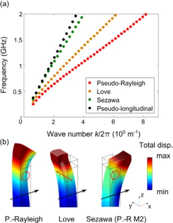
Figure 6(a) presents the band diagram of the first unit cell as well as (b) the distribution of displacements for three dif-ferent eigenmodes. Calculations are performed for a propaga-tion in the x direcpropaga-tion. Due to the symmetry of the structure, and of the crystallography of tungsten, the same results are obtained for a propagation in the y direction. In the dispersion curves, only the four first eigenmodes are shown. They consist of the three first SAWs and the first bulk mode. The first mode corresponds to the pseudo-Rayleigh wave, as experimentally observed. This mode is polarized in the sagittal plane, with a counter clockwise rotation of its polarization regarding to the direction of propagation. The calculated group velocity of the wave at k/2π = 3 × 10⁵ m−1 is v
x = vy = 2130 m s−1,
which is close to the experimental data. An inflexion point located at around k/2π = 3 × 10⁵ m−1 is visible on the disper-sion of this mode. This transition is linked to the stacking of the two materials: at low wave numbers, the propagation of the pseudo-Rayleigh wave is deeply linked with the silicon substrate, whereas for higher wave numbers, the wave is more confined in the tungsten part and the influence of the silicon substrate is negligible. The location of the inflexion point is straightforwardly connected to the tungsten thickness, which
may experimentally vary and may contribute to the differ-ences between experimental and numerical speeds. Moreover, it is well known than thin films properties are slightly different than bulk ones. The second mode is the Love wave, namely the pseudo-shear wave polarized in the y direction. This mode is not experimentally observed either due to the source, for which its symmetry may not allow its excitation or because of the detection process. The third mode is the Sezawa mode (Rayleigh M2). It is similarly polarized to the pseudo-Rayleigh mode, but the polarization turns in the other direc-tion (clockwise regarding to the direcdirec-tion of propagadirec-tion). Again, this mode is not experimentally observed because of the symmetry of the source and/or it is too close to the fourth mode as well. Such a mode (black in the dispersion diagram) is the skimming longitudinal mode, which is the slowest bulk mode. The displacement of this mode is not shown as it is sensitive to the bottom boundary condition of the silicon sub-strate. Yet, the dispersion of this mode seems to be in good agreement with the experimental dispersion measured for the second mode.
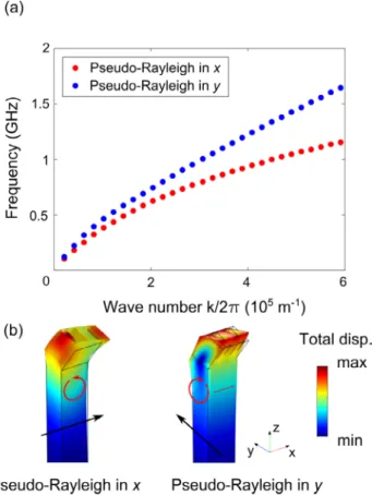
Figure 7(a) presents the dispersion of the two pseudo-Ray-leigh mode following the x (red) and y (blue) directions, as well as their displacements (figure 7(b)) calculated for the second unit cell. Whereas the pseudo-Rayleigh mode corresponds to the first eigenmode for the propagation following x, it cor-responds to the second eigenmode for the propagation in the y direction. A small transverse polarization along the x direc-tion is noted for this Rayleigh mode (propagating following the y direction), coming from the inclination of the holes. Yet, calcul ations were also done for a structure with the same straight holes. The second eigenmode (following the y direc-tion) was also found to be the pseudo-Rayleigh one, without any x polarization, corroborating the study of this mode for the second unit cell. A strong anisotropy is obtained between the two directions, as well as a more pronounced disper-sion. The calculated group velocities at k/2π = 3 × 10⁵ m−1 are vx = 1720 m s−1 and vy = 2350 m s−1, which gives an
aniso tropy ratio of 73%. The propagation of the modes is highly affected by the implementation of the holes, which lead to their folding. Anisotropy has to be linked to the rectangular shape of the holes, which does not similarly disturb the prop-agation of the waves in the two directions. Supplementary simulations, not shown in this paper, were carried out to study the influence of the different geometrical parameters. Results showed that the key parameter in the folding of the mode propagating in the x direction is the length of the hole regarding to the period a. Very similar results were found for the same structure with the same holes, but normally dug to the silicon surface, meaning that the inclination only plays a little role in the anisotropy. As a result, the driving force remains the shape of the holes and the choice of the period a. It is interesting to note that the speed at k/2π = 3 × 10⁵ m−1 of the pseudo-Rayleigh wave propagating following the y direction is slightly higher than the one propagating in the homogeneous tungsten block. At this given wavevector, the wave is not confined in the tungsten block and the silicon still influences the propagation, as shown in the distribution of displacement. Hence, by removing a part of tungsten (holes Figure 6. (a) Calculated band diagram of the first unit cell. Only
the four first modes are shown on the band diagram. (b) The distributions of displacement of the three first modes are shown for a wave number k/2π = 3 × 10⁵ m−1. The colors indicate the total displacement. The black arrow indicates the direction of propagation and the red arrow the polarization.
created, as shown in figure 5), where the dimensions of the holes are in the order of magnitude of the wavelength, the influence of silicon substrate becomes more significant, which may explain the higher group velocity of the pseudo-Rayleigh wave in the y direction (Rayleigh wave velocity in silicon being higher). This effect, in the case of the propagation in the x direction, is small compared to that of the folding of the mode (branch flattens) and does not substanti ally influence the reduction of the velocity in the x direction.
Finally, although the anisotropy was shown to be linked with the holes implemented in the model, the speed decrease of both waves is not explained with this model. It is well known that the GLAD deposition with high angles (α > 70°) leads to a voided material, with a given size and shape distribution of the holes [24]. In the simulation model, only the bigger holes (micrometer scaled) were taken into account. However, the smaller holes also have an influence on the wave propagation. Since Biot [30] in 1956, several groups studied the influence of the porosity on the propagation of elastic waves. Former investigations focused on doped porous silicon wafers report that velocities of longitudinal and shear wave (bulk waves) agree with the following power law [31–33]:
v = v0(1 − p)t
(2)
with v0 the velocity of the bulk wave in the homogeneous material (m s−1), p the porosity of the material, and t, an empirical parameter, depending on the nature of the wave, the porosity [33, 34], and the material. It is likely that the porous tungsten deposited by the GLAD technique follows a similar law, which would strongly reduce the velocities obtained in the model presented and thus explain the experimental veloci-ties reductions.
5. Conclusion
In summary, we have performed measurements of the sur-face acoustic wave propagation in conventional and inclined columnar tungsten thin films by means of a femtosecond heterodyne pump-probe setup. For conventional films, skim-ming longitudinal and pseudo-Rayleigh waves with a strong dispersion have been observed. The highest surface wave velocity was measured in every direction for these films (more than 3750 m s−1), which is 40% higher than in bulk tung-sten and assigned to the contribution of the silicon substrate. The GLAD tungsten films with an inclined columnar micro-structure along the x axis exhibit a reduced velocity (−61% and −27% at k/2π = 3 × 10⁵ m−1 following x and y direc-tions, respectively) compared to conventional films. It has mainly been attributed to the porous structure produced by atomic shadowing effect during the film growth. In addition, the inclined columnar tungsten films give rise to anisotropic behaviors of acoustic wave propagation. The highest velocity has been obtained following the direction perpendicular to the column growth (y direction). It was connected to the aniso-tropic microstructure of the columns. Elliptical cross-sec-tions of the inclined columns develop as the film thickness increases leading to elongated chains on the top, connected to each other and thus, leading to a significant film plane aniso-tropy. The finite element method was used to simulate the two samples. Simulations implied that the anisotropy is linked to the micrometer scaled holes, whereas the speed reduction is assigned to a nano-porosity inside the columns. Moreover, the anisotropy was connected to the holes geometry, especially their form factor and the choice of the period, the column tilt having only a limited influence. The work presented here substantiates the prospect of creating porous and anisotropic architectures in GLAD thin films as a key feature for an inte-gration in devices such as MEMS, NEMS, sensors or actua-tors requiring structural and thus anisotropic properties. Acknowledgments
This work was supported by the Region of Franche-Comté, the French RENATECH network and performed in coop-eration with the Labex ACTION program (contract ANR-11-LABX-01-01). This research was also sponsored by the French National Agency for Research (ANR) funds through the PHEMTO project. The authors also thank the BQR ENSMM for financial support through the COSET project.
Figure 7. (a) Calculated band diagram of the second unit cell for the x and y directions. Only the pseudo-Rayleigh modes are shown on the band diagram. (b) The distributions of displacement of the pseudo-Rayleigh modes propagating in the two directions are shown for a wave number k/2π = 3 × 10⁵ m−1. The colors indicate the total displacement. The black arrow indicates the direction of propagation and the red arrow the polarization.
ORCID iDs
E Coffy https://orcid.org/0000-0002-0671-6398
N Martin https://orcid.org/0000-0003-4730-2578
References
[1] Sugawara Y, Wright O B, Matsuda O, Takigahira M, Tanaka Y, Tamura S and Gusev V E 2002 Watching ripples on crystals
Phys. Rev. Lett.88 185504
[2] Rovira P I, Yarussi R A, Collins R W, Messier R, Venugopal V C, Lakthakia A, Robbie K and Brett M J 1997 Transmission ellipsometry of a thin-film helicoidal bianisotropic medium Appl. Phys. Lett. 71 1180–2 [3] Zhu H and Semperlotti F 2016 Anomalous refraction of
acoustic guided waves in solids with geometrically tapered metasurfaces Phys. Rev. Lett. 117 034302
[4] Lane C 2014 The Development of a 2D Ultrasonic Array
Inspection for Single Crystal Turbine Blades (Cham:
Springer) ch 2, p 15
[5] Krausch G and Magerle R 2002 Nanostructured thin films via self-assembly of block copolymers Adv. Mater. 14 1579–83 [6] Dietiker M, Buzzi S, Pigozzi G, Loffler J F and Spolenak R
2011 Deformation behavior of gold nano-pillars prepared by nanoimprinting and focused ion-beam milling Acta
Mater.59 2180–92
[7] Sanchez C, Boissiere C, Grosso D, Laberty C and Nicole L 2008 Design, synthesis and properties of inorganic and hybrid thin films having periodically organized nanoporosity Chem. Mater. 20 682–737
[8] Barranco A, Borras A, Gonzalez-Elipe A R and Palmero A 2016 Perspectives on oblique angle deposition of thin films: from fundamentals to devices Prog. Mater. Sci. 76 59–153 [9] Robbie K, Brett M J and Lakhtakia A 1996 Chiral sculptured
thin films Nature 384 616
[10] He Y, Zhao Y and Wu J 2008 The effect of Ti doping on the growth of Mg nanostructures by oblique angle codeposition
Appl. Phys. Lett.92 063107
[11] Briley C, Schmidt D, Hofmann T, Schubert E and Schubert M 2015 Anisotropic magneto-optical hysteresis of permalloy slanted columnar thin films determined by vector
magneto-optical generalized ellipsometry Appl. Phys. Lett. 106 133104
[12] Vick D and Brett M J 2006 Conduction anisotropy in porous thin films with chevron microstructures J. Vac. Sci. Technol. A 24 156–64
[13] Stempflé P, Besnard A, Martin N, Domatti A and Takadoum J 2013 Accurate control of friction with nanosculptured thin coatings: application to gripping in microscale assembly Tribol. Int.59 67–78
[14] Malvadkar N A, Hancock M J, Sekeroglu K, Dressick W J and Demirel M C 2010 An engineered anisotropic
nanofilm with unidirectional wetting properties Nat. Mater. 9 1023–8
[15] Hawkeye M, Taschuk M T and Brett M J 2014 Glancing Angle
Deposition of Thin Films—Engineering the Nanoscale
(Chichester: Wiley)
[16] Dilhaire S, Claeys W, Rampnoux J M and Rossignol C 2008 Optical heterodyne sampling device US Patent US 2008/0251740 A1
[17] Abbas A, Guillet Y, Rampnoux J M, Rigail P, Mottay E, Audoin B and Dilhaire S 2014 Picosecond time resolved opto-acoustic imaging with 48 MHz frequency resolution
Opt. Express22 7831–43
[18] Cahill D G 2004 Analysis of heat flow in layered structures for time-domain thermoreflectance Rev. Sci. Instrum. 75 5119–22
[19] Nakamura N, Ogi H and Hirao M 2004 Elastic constants of chemical-vapor-deposition diamond thin films: resonance ultrasound spectroscopy with laser-Doppler interferometry
Acta Mater.52 765–71
[20] Thornton J A 1974 Influence of apparatus geometry and deposition conditions on structure and topography of thick sputtered coatings J. Vac. Sci.
Technol.11 666–70
[21] Anders A 2010 A structure zone diagram including plasma-based deposition and ion etching Thin Solid Films 518 4087–90
[22] Tait R N, Smy T and Brett M J 1992 Structural anisotropy in oblique-incidence thin metal films J. Vac. Sci. Technol. A 10 1518–21
[23] Smith D O, Cohen M S and Weiss G P 1960 Oblique-incidence anisotropy in evaporated permalloy films J. Appl.
Phys.31 1755–62
[24] Mason W P and Thurston R N 1970 Physical Acoustics:
Principles and Methods vol 6 (New York: Academic)
p 136
[25] Paik S M, Kim S and Schuller I K 1991 Surface kinetics and roughness on microstructure formation in thin-films Phys. Rev. B 43 1843–6
[26] Vick D, Smy T and Brett M J 2002 Growth behavior of evaporated porous thin films J. Mater. Res. 17 2904–11
[27] Van Popta A C, Cheng J, Sit J C and Brett M J 2007 Birefringence enhancement in annealed TiO2 thin films
J. Appl. Phys.102 013517
[28] Martin N, Sauget J and Nyberg T 2013 Anisotropic electrical resistivity during annealing of oriented columnar titanium films Mater. Lett. 105 20–3
[29] Taschuk M T, Hawkeye M and Brett M J 2010 Glancing Angle Deposition in Handbook of Deposition Technologies for
Films and Coatings 3rd edn, ed P M Martin (Burlington:
Elsevier) p 621
[30] Biot M A 1956 Theory of propagation of elastic waves in a fluid-saturated porous solid. II. Higher frequency range
J. Acoust. Soc. Am.28 179–91
[31] Da Fonseca R J M, Saurel J M, Foucaran A, Camassel J, Massone E, Taliercio T and Boumaiza Y 1995 Acoustic investigation of porous silicon layers J. Mater. Sci. 30 35–9
[32] Reinhardt A and Snow P A 2007 Theoretical study of acoustic band-gap structures made of porous silicon Phys. Status
Solidi204 1528–35
[33] Aliev G N, Goller B and Snow P A 2011 Elastic properties of porous silicon studied by acoustic transmission spectroscopy J. Appl. Phys. 110 43534–41
[34] Andrews G T, Polomska A M, Vazsonyi E and Volk J 2007 Brillouin light scattering from porous silicon films and multilayers Phys. Status Solidi 204 1372–7