HAL Id: cea-01376554
https://hal-cea.archives-ouvertes.fr/cea-01376554
Submitted on 5 Oct 2016
HAL is a multi-disciplinary open access
archive for the deposit and dissemination of
sci-entific research documents, whether they are
pub-lished or not. The documents may come from
teaching and research institutions in France or
abroad, or from public or private research centers.
L’archive ouverte pluridisciplinaire HAL, est
destinée au dépôt et à la diffusion de documents
scientifiques de niveau recherche, publiés ou non,
émanant des établissements d’enseignement et de
recherche français ou étrangers, des laboratoires
publics ou privés.
DRC 2 : Dynamically Reconfigurable Computing Circuit
based on Memory Architecture
Kaya Can Akyel, Henri-Pierre Charles, Julien Mottin, Bastien Giraud, Suraci
Grégory, Sebastien Thuries, Jean-Philippe Noel
To cite this version:
Kaya Can Akyel, Henri-Pierre Charles, Julien Mottin, Bastien Giraud, Suraci Grégory, et al.. DRC 2 :
Dynamically Reconfigurable Computing Circuit based on Memory Architecture. IEEE International
Conference on Rebooting Computing, Oct 2016, San Diego, France. �cea-01376554�
DRC
2
: Dynamically Reconfigurable Computing Circuit based
on Memory Architecture
Kaya Can Akyel, Henri-Pierre Charles, Julien Mottin, Bastien Giraud, Grégory Suraci, Sébastien Thuries and Jean-Philippe Noel CEA, LETI, MINATEC Campus, F-38054 Grenoble, France,
Univ. Grenoble Alpes, F-38000 Grenoble, France [email protected]
Abstract—This paper presents a novel energy-efficient and
Dynamically Reconfigurable Computing Circuit (DRC²) concept based on memory architecture for data-intensive (imaging, …) and secure (cryptography, …) applications. The proposed computing circuit is based on a 10-Transistor (10T) 3-Port SRAM bitcell array driven by a peripheral circuitry enabling all basic operations that can be traditionally performed by an ALU. As a result, logic and arithmetic operations can be entirely executed within the memory unit leading to a significant reduction in power consumption related to the data transfer between memories and computing units. Moreover, the proposed computing circuit can perform extremely-parallel operations enabling the processing of large volume of data. A test case based on image processing application and using the saturating increment function is analytically modeled to compare conventional and DRC²-based approaches. It is demonstrated that DRC²-based approach provides a reduction of clock cycle number of up to 2x. Finally, potential applications and must-be-considered changes at different design levels are discussed.
Keywords—in-memory computing, computing architecture, programmable logic
I. INTRODUCTION
The growing speed gap between memories and computing units in Von Neumann architecture, also known as the “memory wall”, has led to many research on associative memory circuits and alternative computing architectures [1][2]. Register-heavy solutions were one of the approaches developed in order to overcome this bottleneck without any fundamental changes in processor architecture. The well-known Graphical Processing Units (GPU) are a good example of computing circuits using a register-heavy memory hierarchy (few Mb of register files compared to few Kb in a mainstream CPU) including a very large number of registers files (RF), which allow highly-parallel computing. Moreover, the architecture of SRAM-based RFs itself is also optimized and multi-port bitcells are introduced offering simultaneous read (RD) and write (WR) operations [3][4] to further increase the computing speed. However, parallelization of many computing units and the resulting high throughput of the data leads to a high power consumption [5]. Indeed, with the increase of wire parasitic elements at each new technology node (due to the shrink of the metal routing pitch), the power dissipated by the large amount of data moving between memories and computing units across these highly-parasited wires becomes more and more critical. This resulting high power consumption is seen as one of the principal constraint in contemporary embedded circuit design. As an example, fetching operands in a 28nm nVidia GPUs costs more than computing the operation itself. Thus, this ratio can rise up
to 1000x depending on the location of the data to be fetched in the on-chip memory hierarchy [6][7]. As a result, decreasing data-transfer related power has become a hot research topic. Shortening the physical distance between memories and processing elements thus appears as a relevant solution to reduce the total wire length and thus the overall power consumption. Processing-in-Memory (PIM) concept [8] has been introduced for this purpose to bring the processing elements into the same die as DRAM, thus addressing primarily to off-chip memories. PIM concept, which limits both the latency between memory
Figure 1 a) Conventional computing architecture vs. b) in-memory computing architecture. Moving into In-memory computing should allow speed increase, total area saving and less power consumption since physical distance between memory and computing unit is drastically reduced.
RAM/Reg. Files OUTPUT DFF/LATCH INPUT DFF/LATCH ALU sequencer MUX IN/OUT DFF/LATCH SRAM bitcell array MUX (optional) m u lt i-ro w se le ct o r (2 o r > ) CTRL ALU-like sequencer IN OUT CONTROL IN OUT
DRC²
OUTPUT DFF/LATCH INPUT DFF/LATCH CONTROLa)
b)
and processing unit and the resulting dissipated power, has been reborn recently thanks to the 3D stacking [9]. Some works, as in [10], investigated similar approach for on-chip SRAM circuits, which are used as processor caches due to their significantly higher speed (compared to DRAM). With the rise of emerging NVM technologies, memristor-based material implication (IMPLY) function is proposed to perform Computing-in-Memory (CiM) [11][12], enabling same physical location for both storage and computing. However, memristor-based IMPLY results in destructive operations meaning that the initially stored data is lost after computing.
Another way to drastically increase the computing speed, while not increasing overall power (and area), is to use alternative non-Von Neumann architectures [13]. A suitable architecture for an energy-efficient computing also requires re-configurability since rising chip development costs make workload specific chips very expensive products [14]. At this end, Intel announced that the latest version of their Xeon server chip will have an integrated FPGA to boost performance under workloads requiring optimized processing. An important point in the literature is that SRAM circuits are discarded for long time and spared from any modification, while solutions are sought in high-level design. This is probably because SRAM bitcell arrays are designed with the most aggressive design rules in a given technology and suffer from stability issues due to the process variability. Thus, any change in the array can lead to a highly complex manufacturability issues. However, the need for more optimizations to significantly increase the computing speed at the same time with re-configurability encouraged redesign of SRAM macros with novel features such as in-memory logic function operations [15].
In this work, the CIM concept is pushed one step further and a novel computing circuit is proposed enabling in-memory logic and arithmetic operations exploiting the architecture of SRAM macro, thus lowering data transfer between memory and computing unit (i.e. ALU), as shown in Figure 1. The proposed Dynamically Reconfigurable Computing Circuit (DRC2) can perform the same logic and arithmetic operations as a basic ALU
and, therefore enables non-destructive computing and storage in the same unit. Owing to this approach, we expect significant gains in power consumption and thus pave the way for new opportunities in computing, in particular by using the dynamic reconfigurability since operations are computed in-situ, without using “frozen” dedicated computing circuits based on logic gates.
The paper is structured as follows: The section II introduces the concept of proposed DRC². The section III presents the 3-port 10T bitcell used in the SRAM array and how different logic and arithmetic operations can be performed. Then a representative test case based on DRC² for imaging processing is discussed in section IV. Perspectives for the proposed concept are briefly discussed in section V. Finally, section VI concludes the paper.
II. DYNAMICALLY RECONFIGURABLE COMPUTING CIRCUIT
(DRC²)CONCEPT
Figure 3 presents the DRC² concept. It is based on a SRAM bitcell array in which multiple rows can be selected in the same time during the same clock cycle for performing in-situ operations between selected rows [15]. The operation type is chosen and controlled slice-wise (using a dedicated controller, as shown in Figure 3), thus different operations can be performed on different slices of the same array offering highly-parallel operations. For the rest of the paper, the term “memory slice” is used to describe a memory column with some selected bitcells and the associated column peripheral circuitry. The results coming from a given memory slice can be read as in any conventional memory circuit, or can be written-back (WB) into the memory in the same or next clock cycle.
Table 1 presents the list of 19 basic operations that can be performed by the proposed DRC². It enables to perform these operations inside the memory, thus limiting intensive data transfert. Operations like RD, RD_NOT, RD_0 and RD_1 are natively present in a conventional memory circuit (or can be added without any complexity), unlike to the others. As shown in Figure 3, the SRAM bitcell array is accessed through multiple rows in the same time in the same clock cycle, which is indeed prohibited in a conventional memory circuit to ensure a proper read. The multiple row access being the key for computing inside the memory circuit, it is worth to say that the intelligence
Figure 2 10-Transistors (10T) SRAM bitcell including one Write-Port (WP) and two Read-Port (RP), False (F) and True (T). Each RP is formed by its pass-gate (PG) and its pull-down (PD) transistors.
R B LF R B LT BLFI BLTI W B LT W B LF WWL RWLT RWLF RPF RPT WP (6T SRAM) PGT PGF RPF_PD RPF_PG RPT_PG RPT_PD
Figure 3 Proposed Dynamically Reconfigurable Computing Circuit (DRC²) based on 3-Port SRAM bitcell. Instead of delivering the stored content, the output bus delivers computed metadata.
X O R N A N D O R A N D Selected operations <N-1:0> Selected rows <M-1:0> output bus <N-1:0> MxN SRAM Bitcell Array
N O P N O P N O P N O P N O P N O P R1<N-1:0> R4<N-1:0> RM-2<N-1:0> RM-3<N-1:0> 0 1 1 1 1 0 0 1 1 0 0 1 0 0 1 0 1 0 1 0 1 0 0 1 1 0 0 0 1 0 N O P N O P N O P A N D N A N D N O P N O P N O P N O P X O R A N D N O R A N D N A N D N O P N O P N O P N X O R X O R Cycle1 Cycle2 Cycle3 Cycle1 Cycle2 Cycle3
controller
N O Pcomes from both the bitcell array access and the associated peripheral circuitry.
III. DESCRIPTION OF OPERATIONS ENABLED BY DRC² Figure 2 presents the 10-Transistors (10T) SRAM bitcell used in the array. It is composed of one 6T write-port (WP) and two 2T read-port (RP). Internal nodes BLTI (stores data) and BLFI (stores complemented data) of WP are connected to RP False (RPF) and RP True (RPT), respectively, allowing isolation of read and write operations. Both RPs are connected to their proper read bit-lines (RBLF and RBLT, respectively), through
pass-gate (PG) transistors RPF_PG and RPT_PG. RPF and RPT are connected through pull-down (PD) transistor RPF_PD and RPT_PD to ground line GND.
This 10T SRAM bitcell is accessed through three Word-Line (WL) signals, as shown in Figure 2: Write WL (WWL), Read WL True (RWLT and Read WL False (RWLF). WWL allows accessing internal nodes of 6T WP, thus used for write operation (WR). WR is performed as in any conventional SRAM by activating corresponding WWL and driving WBLs at the values to be written in the bitcell. RWLT allows selecting RPT, thus reading the stored data through BLFI without a risk of an
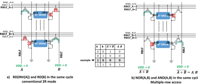
Figure 4a) Dual access to memory slice (through RPF and RPT) allowing to perform RD(NOT(A)) and RD(B) on RBLF and RBLT, respectively. b) Multiple access through RPF and RPT allowing to perform NOR (A,B) operation on RBLF and AND(A,B) operation on RBLT. For the sake of simplicity, only NOR and AND operations with two operands are shown. Both operations can be performed with up to M operands where M is the column length.
6T SRAM/A=0 A=1 WWL_A=0 RWLT_A =0 RWLF_A=1 6T SRAM R B LF R B LT /B=1 B=0 WWL_B=0 RWLT_B=1 RWLF_B=0
a) RD(INV(A)) and RD(B) in the same cycle conventional 2R mode 6T SRAM/A=0 A=1 WWL_A=0 RWLT_A =1 RWLF_A=1 6T SRAM R B LF R B LT /B=1 B=0 WWL_B=0 RWLT_B=1 RWLF_B=1
b) NOR(A,B) and AND(A,B) in the same cycle Multiple-row access A B 0 0 1 0 0 1 0 0 1 0 0 0 1 1 0 1 VDD -> 0 VDD -> 0 VDD -> 0 VDD -> 0 example TABLE I
Operation Description # of operands # of cycle Operation Type
RD/BUFF Read the content of selected bitcell 1 1 Memory
RD_NOT/IN V
RD the complementary content of selected bitcell 1 1 Memory
RD_0 Read as “0” the selected bitcell 1 1 Memory
RD_1 Read as “1” the selected bitcell 1 1 Memory
XOR/ COMP
Exclusive OR if #of operands =2 Comparison if # of operands >2
N 1 Logic
NXOR NOT Exclusive OR N 1 Logic
NOR NOT-OR N 1 Logic
NAND NOT-AND N 1 Logic
OR OR N 1 Logic
AND AND N 1 Logic
IMP Materiel Implication N 1 Logic
SHIFT Shift the bitcell content to left or right 1 2 Logic/Arithmetic
ADD Addition 2 3 Arithmetic
SUB Subtraction 2 4 Arithmetic
INC Increment by 1 1 3 Arithmetic
DEC Decrement by 1 1 3 Arithmetic
GT Greater than 2 2 Arithmetic
LT Less than 2 2 Arithmetic
Table 1 List of operations, their description, number of maximum operands, number of minimum cycles that is needed to perform these operations and operation family that they are belonging.
unwanted data flip inside the WP (read disturb phenomena [17]), while RWLF allows reading the complemented data through BLTI and RPF. The used nomenclature for RPT and RPF comes from following: BLTI stores the true data and BLFI stores the complemented data, i.e. false data. The value read through RPF is data stored in BLFI, while the data read through RPT is data stored in BLTI.
In this work, the 10T SRAM bitcell is chosen since we consider that it is the most efficient bitcell for the proposed computing circuit. However, any other bitcell allowing differential read (single-port 6T, dual-port 8T, etc.) can be used for the same purpose at the expense of not being able to perform write and read in the same clock cycle, which impacts the overall number of cycles depending on the desired operations.
RD, NOR/OR and AND/NAND operations Figure 4.a illustrates a conventional dual RD operation in 10T SRAM memory slice through both RPs: RBLF and RBLF are pre-charged to VDD prior to the operation. The bitcell A is selected by activating (from 0 to 1) RWLF_A and the bitcell B is selected by activating RWLT_B, while other RWLs are kept low. Which means that all pass-gate transistors are OFF in the relevant memory column except RPF_PG of bitcell A and RPT_PG of bitcell B. In this example, bitcell A stores a ‘1’ (BLTI=VDD, BLFI=GND), and bitcell B stores a ‘0’ (BLTI=GND, BLFI=VDD). As a result, RPF_PD of bitcell A and RPT_PD of bitcell B are both ON and lead to the discharge of RBLF and RBLT, respectively through RPs. In other words, the final voltage level of RBLF is equal to ̅, while the final voltage level of RBLT is equal to B.
Figure 4.b illustrates the same memory slice bit with multiple row access in which only two bitcells, A and B, are shown. Like a conventional read operation, RBLF and RBLT are pre-charged to VDD. Then, bitcells A and B are accessed through their respective RPF and RPT (RWLF_A = RWLF_B = RWLT_A= RWLT_B=1), while RWLs of other bitcells RPs (not shown in Figure 4) are kept low. The final voltage level on RBLF depends on stored data in bitcell A and in bitcell B (voltage level of BLTI_A and BLTI_B); if at least one of two bitcells stores ‘1’, RBLF will be discharged to ‘0’, if both stores a ‘0’ (BLTI=GND, BLFI=VDD), only RBLF will be kept at VDD. This operation reproduces the truth table of a N-input NOR logic gate. The final voltage level of RBLT is dependent on the complement of the stored data in A and B (voltage level of BLFI). If one of two bitcells stores a ‘0’ (BLTI=GND, BLFI=VDD), RBLT is discharged, which reproduces the truth table of a N-input AND logic gate. Therefore, OR and NAND truth tables can be also reproduced by inverting RBLF and RBLT signals.
It is worth to say that while this example shows two selected bitcells, up to M cells (M is the column length which is equal to the number of rows in the memory array) can be selected in the same column to perform operations with M operands, since the Boolean algebra is associative.
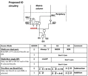
Figure 5 presents the proposed periphery circuitry of memory slice. A cascaded NAND gates architecture together with the MUX control signal ADDEN allow us enabling different logic and arithmetic operations. In detail, ADDEN is set to ‘1’, only when an addition operation (ADD) has to be performed. The
details of arithmetic operations, ADD and subtraction (SUB), are presented later in this section.
XOR/NXOR, COMP, Material Implication (IMP), Less than (LT) and Greater Than (GT) Bitcells in of a given memory slice can be accessed in 3 different ways depending on which operation(s) is (are) targeted. Multiple row selection with dual access to each bitcell allows reading all selected bitcells on both RPs as already depicted in Figure4
.
b. In this access mode, if signal ADDEN=0, periphery outputs O1, O2, O3 are equal to always ‘1’, NXOR and XOR, respectively. If more than two bitcells in the same slice are selected, XOR output yields to a comparison operation (COMP) ; O3 is ‘1’ if at least one among all selected bitcells stores a different data, and NXOR output O2 leads to the opposite test giving ‘1’ if all selected bitcells store same data. The second access mode is as follows: Multiple bitcells in a given memory slice are selected but each one is accessed through only one RP. Supposing that bitcells selected on RPF are F0, F1...Fi and bitcells selected through RPT are T0,T1.…Tk, a NOR is performed between F0,F1...Fi , an AND is performed between T0,T1.…Tk. The output O1 is in this case equal to:… . . … . . . …
… ⋯
This operation is named as “mixed operation” (denoted as mixOP in Figure 5). Moreover, if one bitcell is selected on each RP, for example F0 and T1, output O1 gives , which is equal to material implication (IMP) denoted as T1 → F0. Furthermore, a Boolean expression ̅ is the equivalent of Less Than (LT) operator (A < B). Therefore, LT and Greater Then (GT) operations can be also performed word-wise in the proposed memory circuit with some additional gates in the array periphery; they are not detailed in this paper due to the space limitation.
Figure 5 Periphery control and resulting outputs under different access modes. RBLF RBLF RBLT RBLT ADDEN 1 0 Matrix column Periphery O1 O3 O2
Access Mode ADDEN O1 O2 O3 Comment
Multi-row dual port: Both RPs of N selected bitcells are ON
0 Always ‘1’ NXOR XOR
1 Don’t Care
Multi-Row single-RP: Only one RP is ON for each of the N selected bitcells.
0 mixOP Don’t care
1 Don’t Care
Two-Row one Read-Port: Only one bitcell on each RBL is selected.
0 = B A = A B Subtraction
1 = A+B Addition
Proposed IO circuitry
Addition / Subtraction
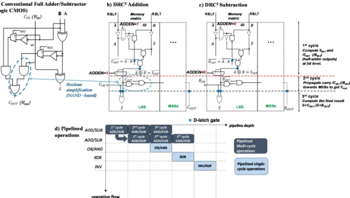
The last access mode denoted as two-rows-single RP, is used for arithmetic operations in the proposed circuitry. A Ripple-carry adder/subtractor, which is based on a full-adder/subtractor is implemented in the memory slice periphery allowing us to perform addition and subtraction between two K-bits word that is previously stored in the memory. A schematic of conventional a full adder/subtractor is shown Figure 6.a, which is composed of XOR, AND and OR logic gates.
Assuming bitcell A is selected through RPF thus final RBLF value is equal to ̅, and bitcell B is selected through RPT thus the final RBLT value is equal to B. If ADDEN equals to ‘1’, a half-adder, which consists of an AND gate to compute carry (C) and a XOR gate to compute summary (S) of the addition between operands A and B, is realized in one clock cycle. Setting ADDEN to ‘0’ allows reproducing a half-subtractor; this time the carry output becomes the borrow output (B), which is equal to ̅. . We modified the full-adder equation in order to replace the series of AND and OR gates by two NAND gates, as depicted in Figure 6.bin the circled area. This has the following benefits: Overall number of transistor decreases minimizing periphery area in the same time increasing speed, since number of stages to cross are reduced from 4 to 2. Therefore, the carry (borrow) of the current slice, C (B), has to be read as ̅ ( ,), which corresponds to a NAND between operands (instead of the AND as in a full adder). The following part describes implementation of a adder; the same is valid for full-subtractor by replacing C (carry) with B (borrow).
A full adder can be therefore reproduced by propagating carry to columns storing LSBs of tow K-bit words. Figure 6.b presents how a ripple-carry adder is reproduced in memory slice allowing addition of two K-bit words. A single ADD can take 3 clock cycles for high-frequencies (>GHz). In the first cycle, half-additions are executed; the output carry Cout_j and sum Sj of memory slice j are latched. In the second cycle, Cout_j is propagated to the next slice (from LSB to MSB) allowing updating Cout_j+1, and the updated Cout_j+1 is latched. This carry propagation is illustrated in Figure 6.b as the input carry Cin. Figure 6.c presents how a ripple-carry subtractor is reproduced in memory slice and borrows are propagated as the same way as a ripple-carry adder but setting ADDEN to ‘0’.
Figure 6.d presents our pipelined ADD/SUB approach in which successive ADD/SUB area added in pipeline depth. One new operation can be added in the pipeline at every new clock cycle without any latency thanks to the 2R1W 10T SRAM bitcell. Finally, increment (INC) and decrement (DEC) operations can also be performed, since they correspond to ADD 1 and SUB 1, respectively.
Shift Operation
Shift operation can be implemented in the proposed memory circuit by adding latches in the array periphery in order to implement a conventional CMOS shifter circuit. This part is not detailed in this paper.
Figure 6 a) Conventional CMOS logic Full-adder/subtractor, full-adder/subtractor based on ripple-carry adder/subtractor architecture implemented in DRC² slice periphery IO b) for addition and c) for subtraction. A single ADD/SUB of 2 words of K bits last for 3 clock cycles. When signal ADD=1, circuit performs ADD operations, else it performs SUB operations. d) Pipelined operations in DRC², different cycles of multi-cycle ADD/SUB operations can be pipelined together with single-cycle operations like OR, AND, XOR.
IV. RESULTS:IMAGE PROCESSING APPLICATION
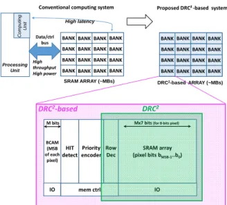
In modern robotic applications, the environment is modeled using occupancy grids [20]. Such grids encode occupation information using signed binary words (e.g. 8-bit words) [21]. The occupation data is then manipulated by the application as a simple mono-channel image buffer. To perform obstacle detection and velocity estimation, Bayesian occupancy filters are used. Such filters allow to estimate and predict occupancy over time. To do so, prior state (image buffer at time t-1) is mitigated then fused with current state (image buffer at time t). The mitigation can typically be implemented by looking at the
sign of the data. If it is positive (bit 0) the data as to be decremented (by 1 or another constant value). If it is negative (bit 1), the data has to be incremented (by the same value). Figure 7 presents on the top left a conventional system using a processing unit and a dedicated SRAM array for pixel storage, in which we can assume that the saturating increment is performed as following: Pixel values which are previously converted into signed 8-bits words are stored in a memory array. The processing unit reads sequentially each pixel and check the sign bit. Depending on the sign bit, pixel value is incremented or decremented and the new value is written back to the memory. In order to store the entire image, relatively large SRAM arrays are required which results in latencies while reading from and writing to the memory depending on the addressed memory bank location. In this work, we assume 1 latency cycle for both read and write as an average latency which may be seen as an optimistic approach. Assuming a 1RW 6T SRAM bitcell, as usually used in many microcontrollers, 1 clock cycle for read, 1 clock cycle for sign test, 1 clock cycle for increment/decrement, 1clock cycle for write back and 2 clock cycles due to latencies are required, in total leading to an overall of 6 clock cycles for one pixel. Figure 8.a presents pipelined operation flow using 1RW 6T SRAM bitcell, in which read and write operations cannot be performed in the same clock cycle. 6 clock cycles are needed to process one pixel, and each new pixel would add 3 more cycles at the end of the pipeline depth. The overall number of cycles depends on the number of pixels in the picture, Np, and is equal to 3*Np+3. Figure 7 also presents the proposed system based on DRC2 architecture coupled with a Binary Content Addressable Memory (BCAM) [15]. BCAM circuits are hardware-based search engines allowing to perform search of the memory
Figure 8 Pipeline stages for performing saturating increment in a pixel array using different mentioned systems. a) Conventional system using 1RW 6T SRAM, b) DRC2-based system using 1RW 6T SRAM bitcell, c) DRC2-based system using 2R1W 10T SRAM bitcell.
pipeline depth operation flow RD TEST INC/DEC INC no:1 INC no:2 INC no:3 INC no:4 INC no:5 a) 6T Bitcell (1RW) based conventional
Total number of cycles for N pixels= 3*N+3
WR RD TEST INC/DEC WR RD TEST 1stcycle INC/DEC 2ndcycle INC/DEC 3rdcycle INC pipeline depth operation flow 1stcycle INC/DEC 2ndcycle INC/DEC 3rdcycle INC/DEC INC no:1 INC no:2 1stcycle INC/DEC NOP NOP NOP INC no:3 INC no:4 INC no:5 1stcycle INC 2ndcycle INC pipeline depth operation flow 1stcycle INC 2ndcycle INC 3rdcycle INC 1stcycle INC INC no:1 INC no:2 INC no:3 INC no:4 INC no:5 c) 10T Bitcell (2R1W) based DRC2 b) 6T Bitcell (1RW) based DRC2
Same pipeline repeated starting with SR ‘0’. Total number of cycle for N pixels = N+8 Same pipeline repeated starting with SR ‘0’
Total number of cycle for N pixels = 2*N+6
SR ‘1’ encode encode encode SR ‘1’ encode encode encode encode LATENCY LATENCY LATENCY
Figure 7 Conventional system based on a processing unit and SRAMs on the top left, and the proposed computing system circuit using DRC2 architecture coupled with a BCAM.
IO mem ctrl SRAM array (pixel bits bMSB-1..b0) Row Dec BCAM (MSB of each pixel) HIT detect Priority encoder DRC2 Data/ctrl bus High throughput High power
Mx7 bits (for 8-bits pixel)
M bits IO BANK BANK BANK BANK
BANK BANK BANK BANK BANK BANK BANK BANK BANK BANK BANK BANK
SRAM ARRAY (~MBs) High latency Processing Unit C o m p u ti n g U n it BANK BANK BANK BANK
BANK BANK BANK BANK BANK BANK BANK BANK BANK BANK BANK BANK
DRC2-based ARRAY (~MBs)
DRC2-based
content, and to match specific data in a single clock cycle. In the proposed system, MSB of each pixel is stored in the BCAM array and the rest of bits of each pixel is stored in the SRAM array. Positive signed pixels are detected by searching ‘1’ in BCAM, while negative signed bits are detected by searching ‘0’. The hit detection bloc outputs lines of BCAM array storing the searched sign bit, i.e. having a search hit. A priority encoder together with the memory controller would allow to sequentially read hits and increment/decrement these lines using the DRC2 increment/decrement function. In other words, given signed pixels are identified in one cycle whatever the image resolution. Priority encoder encodes one hit address and transfers the encoded address to memory controller in one cycle. The encoded hit line is discharged to ‘0’. Memory controller sends address of the pixel that has to be incremented/decremented by 1 to the SRAM array. The same is repeated for the opposite signed bits.
As mentioned before, the SRAM array in DRC2 can be designed with any SRAM bitcell that offers differential read at the expense of overall time depending on the desired operation. Figure 8.b presents the pipeline stages for a DRC2-based system using 1RW 6T SRAM bitcell, in which one search cycle (SR) is performed at the beginning and match line encoding (encode) is performed before each 4-cycles increment/decrement operation. Since computing takes place in-memory, there is no data transmission from the memory array to an external computing unit removing all latency cycles. The DRC2-based system using 6T SRAM bitcell does not allow performing simultaneous WR and RD operations, and therefore a no-operation (NOP) cycle has to be inserted between 1st and 2nd cycles of an INC/DEC, which leads to an overall number of 2*Np+3 cycles..
As shown in section III.C, increment function takes 3 cycles using 2R1W 10T SRAM bitcell and it can be pipelined, as described in Figure 6.d. Figure 8.c presents pipeline stages of saturating increment in the DRC2-based system using 2R1W 10T SRAM bitcell, in which one search cycle is performed at the beginning and the match line encoding is performed before each 3-cycles increment operation. The total number of clock cycle is Np+8 (versus 2*Np+3).
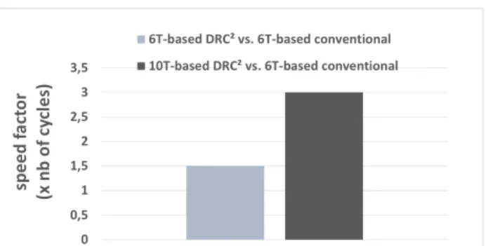
Figure 9 presents the comparison in terms of speed between the conventional system and the DRC2-based system for a given picture resolution. In order to have a fair comparison, DRC2 -based system is considered with both bitcell--based memory arrays. It is shown that, ≈x1.5 speed factor is reached with DRC2-based system using slow-but-small 1RW 6T SRAM bitcell. On the other hand, if 2R1W 10T SRAM bitcell is used in DRC2-based system, ≈x2 speed factor is reached w.r.t the conventional system (since 2R1W 10T SRAM bitcell allows simultaneous WR and RD operations reducing overall number of cycles in the pipeline depth).
In overall, DRC2-based systems help reducing total number of clock cycles in saturating increment/decrement function since latencies due to read from and write to memory banks are canceled by moving computing inside the memory macro. Moreover, although we are not able to quantify the gain at this stage, the suppression of the intensive data transfer between different memory banks and the computing unit, therefore suppression of all flip-flops, buffers and wires, lead to a significant power consumption reduction. In other words, the in-memory computing architecture enabled by the DRC2-based system can offer improvements in power consumption and speed, while replacing the conventional computing architecture by a configurable memory based computing circuit.
V. DISCUSSIONS AND PERSPECTIVES
The Von Neumann programming model, where data and instruction memory accesses are interlaced, has been very successful and a lot of technologies and tools for code generation was build using this model. More specifically, compiler are based on instruction scheduling, memory model (variable in memory, in register, in cache, etc.), data layout, etc. New parallel models such as pipelined instructions, instruction level parallelism (ILP), data parallelism (SPMD) on GPU or asynchronous multicore was already challenging as a programmer point of view and has been a very active research domain. But specific languages such as CUDA for GPU, tools such as OpenMP or OpenACC or specific libraries have tried to help programmers in this difficult task to extract different parallelism level. As said in the introduction, DRC2 will change dramatically the traffic between memory and processing core and the programming model. To the best of our knowledge, there is no specific tools or language able to generate a so high level of parallelism. We can only try to imagine different tasks on how to use this new computing in memory paradigm. We could revisit the work already done on the bit parallel machines from the 90. The Connection Machines [18] and the MasPar was successful machines in term of parallelism usage. It supported *LISP parallel language [19] and the CMFortran which was specific languages. It was in the 90's and even if the available parallelism was important, the programming model was restrictive and difficult to exploit. Maybe work could be done in this direction.
Figure 9 Clock cycle reduction factor between a conventional (using 6T SRAM bitcell) and the proposed DRC2-based system (using 6T and 10T SRAM bitcells). 0 0,5 1 1,5 2 2,5 3 3,5 sp e e d f a ct o r (x n b o f cy cl e s)
6T-based DRC² vs. 6T-based conventional 10T-based DRC² vs. 6T-based conventional
Another analogy come from the "SQL view" notion in databases. The SQL view allow to "see and exploit" the database through a view, which is a transformation from the initial database without modifying the initial database. The transformation can be table join or more complex transformations. We could imagine to use DRC2 in a similar way: the physical memory could be duplicated on a large memory map; each duplication corresponding to a "view". A simple computing core with a large memory system (such as the 128 bits memory from the RISC-V http://riscv.org/) could use a single view to differentiate the operations (XOR, NAND, NOR, ADD). Thus, the program become a set of DMA accesses leading to a complex treatment on big data sets.
We could imagine to add special instruction in a RISC V processor to implement these "special DMA" instruction working on large memory ranges. Of course this kind of memory should not implement a full instruction set but the compute core could also implement control operation as usual. Many applications can benefit from such a memory engine. Immediate idea are:
•Cryptography which are easily implemented as bit operations: For example, systems that are memory intensive such as “OneTimePad”, could be easily implemented with a XOR between two memory locations. The DRC² could implement those algorithms with a great energy efficiency.
•NOSQL Data bases which need a high level of parallelism: These databases need to scan datasets and select matching results. We could imagine a global selection mechanism using binary masks applied on large memory page.
•Image filtering implemented at bit level: is also a good candidate. Section IV shown an initial example of an algorithm that take advantage of the DRC², we could imagine that many pixel level transformation implemented in graphic card (Shadows under windows, mouse cursor masking, etc) could be easily implemented.
Work are under progress to give more realistic examples of algorithms taking advantage of this DRC².
Finally, demand for reconfigurable circuits is on rise, since modern applications should be able to adapt to different operating environments that may require loading new circuits on board. DRC2 offer high flexibility for reconfigurable computing, since logic and arithmetic operations are executed where the data is stored but not using hard-coded gates. A potential application can be in cellular networking, in which circuits should adapt to different network standards such as 3G, 4G and 5G.
VI. CONCLUSION
In this paper, we have presented a novel concept of computing circuit called DRC², exploiting the architecture of SRAM macro. This circuit is able to perform logic and arithmetic operations with very limited data transfer to other circuits enabling a veritable in-memory computing. It should allow overcoming the well-known memory wall bottleneck and reducing data transfer-related excessive power consumption.
As a result, it is well-suited for data-intensive applications. An imaging processing test case based on saturating increment function is presented using both a conventional Von Neumann computing architecture and a DRC2-based system. The results show a significant speed gain (up to x2) by using the novel in-memory computing architecture. Furthermore, we expect a drastic power consumption reduction. DRC2 architecture paves the way for novel computing algorithms that will benefit at maximum from its features, not only for power consumption but also for high reconfigurability and increased speed.
REFERENCES
[1] Wm. A. Wulf, S. A. McKee, “Hitting the memory wall: implications of the obvious”, ACM SIGARCH Comp. Arch. News, Vol 23, (1), pp 20-24, 1995.
[2] M.V. Wilkes, “The memory wall and the CMOS end-point”, ACM SIGARCH Comp. Arch. News, Vol 23, (4), pp.4-6, 1995.
[3] S-F. Hsiao et al., “Design of Low-Leakage Multi-Port SRAM for Register File in Graphics Processing Unit”, ISCAS, pp 2181-2184, 2014. [4] G. Burda et al., “A 45nm CMOS 13-Port 64-Word 41b Fully Associative
Content-Addressable Register File , ISSCC, pp. 286-287, 2010. [5] M. Horowitz, “Computing’s Energy Problem (and what we can do about
it)”, ISSCC, pp 10-14, 2014.
[6] W. Dally, “Power Programmability, and Granularity”, keynote presentation in IPDPS, 2011.
[7] HiPEAC Vision 2015 – www.hipeac.net
[8] M. Gokhale et al., “Procesing in memory: the Terasys massively parallel PIM array”, IEEE Computer, vol 28 (4), pp. 23-31, 1995.
[9] Zhu et al., “A 3D-Stacked Logic-in-Memory Accelerator for Application-Specific Data Intensive Computing”, 3DIC, pp 1-7, 2013.
[10] P. Jain et al., “Intelligent SRAM (ISRAM) for Improved Embedded System Performance”, in proceedings of DAC, 2003.
[11] S. Kvatinsky at al., “Memristor-Based Material Implication (IMPLY) Logic: Design Principles and Methodologies “, TVLSI, vol 22 (10), October, 2014.
[12] S. Hamdioui et al., “Memristor based computation-in-memory architecture for data-intesive applications”, DATE, pp 1718-1725, 2015. [13] P. Dlugosch et al., “An Efficient and Scalable Semiconductor Architecture for Parallel Automata Processing”, IEEE TPDS, Vol. 99, pp. 3088- 3098, 2014.
[14] Mai et al., “Video-Active RAM: A Processor-in-Memory Architecture for Video Coding Applications”, ISCA, pp. 161-171, 2010.
[15] Jeloka et al., “A 28 nm Configurable Memory (TCAM/BCAM/SRAM) Using Push-Rule 6T Bit Cell Enabling Logic-in-Memory”, JSSC,Vol 51 (99), pp 1009-121, 2016.
[16] Shibata et al., ,“A 0.5V 25MHz 1mW 256kb MTCMOS/SOI SRAM for solar-power-operated portable personal digital equipment-sure write operation by using step-down negatively overdriven bit-line scheme”, JSSC, Vol. 41 no.3, pp.728-742, 2006.
[17] Mukhopadhyay et al., “Modeling of failure probability and statistical design of SRAM array for yield enhancement in nanoscaled CMOS”, IEEE TCAD, Vol. 24, no. 12, pp.1859-18880, 2005.
[18] W. D. Hillis, “The Connectino Machine”, published by MIT Press, 1989. [19] Guy L. Steele. Jr. , al., “Connection Machine Lisp: Fine-grained Parallel Symbolic Processing”, Proceedings of the 1986 ACM Conf. on LISP and Functional Programming, pp 279-277.
[20] A. Elfes, “Occupancy grids: a stochastic representation for active robot perception”, Sixth Conference on Uncertainity in AI, 1990.
[21] T. Rakotovao et al., “Multi-Sensor Fusion of Occupancy Grids based on Integer Arithmetic”, IEEE ICRA, 2016.
[22] C. Coué, et al. “Bayesian Occupancy Filtering for Multitarget Tracking: an automative application”, Intl. Journal of Robotics Research, SAGE Publications, Vol 25 (1), pp. 19-30, 2006.

![Figure 3 presents the DRC² concept. It is based on a SRAM bitcell array in which multiple rows can be selected in the same time during the same clock cycle for performing in-situ operations between selected rows [15]](https://thumb-eu.123doks.com/thumbv2/123doknet/12981144.378337/3.892.74.418.141.388/figure-presents-concept-multiple-selected-performing-operations-selected.webp)