HAL Id: cea-02185184
https://hal-cea.archives-ouvertes.fr/cea-02185184
Submitted on 8 Apr 2020
HAL is a multi-disciplinary open access
archive for the deposit and dissemination of sci-entific research documents, whether they are pub-lished or not. The documents may come from teaching and research institutions in France or abroad, or from public or private research centers.
L’archive ouverte pluridisciplinaire HAL, est destinée au dépôt et à la diffusion de documents scientifiques de niveau recherche, publiés ou non, émanant des établissements d’enseignement et de recherche français ou étrangers, des laboratoires publics ou privés.
Distributed under a Creative Commons Attribution| 4.0 International License
Thin layer etching of low-k SiCO spacer using hydrogen
ion implantation followed by hydrofluoric acid
Nicolas Posseme, Maxime Garcia-Barros, François Leverd, Daniel Benoit,
Olivier Pollet, Guillaume Audoit, Cyril Guedj, Audrey Jannaud, S. Barnola
To cite this version:
Nicolas Posseme, Maxime Garcia-Barros, François Leverd, Daniel Benoit, Olivier Pollet, et al.. Thin layer etching of low-k SiCO spacer using hydrogen ion implantation followed by hydrofluoric acid. Journal of Vacuum Science & Technology B Microelectronics and Nanometer Structures, American Vacuum Society (AVS), 2018, 36 (5), pp.052201. �10.1116/1.5038617�. �cea-02185184�
followed by hydrofluoric acid
Nicolas Posseme,1,a)Maxime Garcia-Barros,2François Leverd,2Daniel Benoit,2 Olivier Pollet,1Guillaume Audoit,1Cyril Guedj,1Audrey Jannaud,3and S. Barnola1 1
CEA LETI-Minatec, 17 Avenue des Martyrs, 38000 Grenoble, France
2
ST Microelectronics, 850 Rue Jean Monnet, 38920 Crolles, France
3
Serma Technologies, Minatec Campus, 38040 Grenoble, France
(Received 4 May 2018; accepted 13 July 2018; published 10 August 2018)
Spacer etching realization is considered today as one of the most critical processes for the fully depleted silicon on insulator devices realization. The challenge arises from the fact that low-k spacer needs to be introduced to improve device performances. In this paper, a new approach to etch the low-k SiCO film was investigated. This approach is based on the SiCO film modification by H2plasma followed by a removal step of this modified layer using hydrofluoric acid- (HF) based
wet cleaning. It has been demonstrated that SiCO layer modification depth is controlled by plasma parameters like bias voltage. The SiCO film modification induced by H2 plasma has been well
understood by x-ray photoelectron spectroscopy, infrared spectroscopy analyses in transmission or in multi-internal reflection. It has been demonstrated that the H2plasma exposure converts the SiCO
film in volume into an SiOxHyfilm, explaining the higher damaged film removal rate when dipped
in liquid phase HF. Finally, the compatibility of the new etch approach with the SiCO low-k film has been demonstrated on pattern structures. Published by the AVS.
https://doi.org/10.1116/1.5038617
I. INTRODUCTION
With aggressive device shrinking, parasitic capacitances through the spacer become an important contributor to the total device capacitance. This issue is exacerbated by the common use of silicon nitride (SiN) spacers since SiN has a relatively large dielectric constant (k ∼ 7.5). A simple approach to reduce capacitive coupling through the spacer is to replace it with a low-k material.1Therefore, the reduction of the spacer k value is a key for the high performance devices.
In this context, low dielectric (low-k) constant films like SiOCN, SiCBN, or SiCO have been proposed in the litera-ture to replace the traditional silicon nitride.2–4
But the introduction of these materials leads to critical patterning issues. Such low-k films are much more sensitive to fluorocarbon-based chemistries generally used in fully depleted silicon on insulator technology allowing pattern dimension control and selectivity to the underlying (Si or SiGe) layer.5For example, the spacer low-k film can be iso-tropically etched using CH3F/O2/He plasma leading to a
dif-ficult critical dimension (CD) control during the etch process (Fig.1).
In another case, a full film modification of the low-k film, occurring during the plasma etching process, can lead to a complete removal of this film after hydrofluoric acid (HF) ( pre clean epitaxial step), as shown in Fig.2.
These difficulties impose to optimize the current etch chemistry to be compatible with low-k spacers.
An original etching approach has recently been reported for silicon nitride spacer etching. It consists of anisotropical modification of the silicon nitride film by H2or He plasma
performed in an inductively coupled plasma (ICP) or a
capacitively coupled plasma etch tool and then selectively removing the modified fraction of the layer with hydrofluoric acid dip,5vapor HF,6or NH3/NF3(Ref.7) remote plasma. It
has been demonstrated that layer modification depth is con-trolled by plasma parameters, like bias voltage, source power, and process time. The benefit of this unconventional technique was demonstrated on 14 nm fully depleted silicon on insulator logic device and showed less than 1 nm silicon nitride spacer CD loss, less than 0.6 nm SiGe recess which enabled defect-free source/drain epitaxy.8
In this paper, we propose to investigate the compatibility of this new approach with the etching of SiCO. This low-k film modification has been analyzed by x-ray photoelectron spectroscopy (XPS), and infrared spectroscopy analyses in transmission (T-FTIR) and multiple internal reflection (MIR-FTIR).
Finally, the SiCO film etching has been evaluated on pat-terned structures.
II. EXPERIMENT
A. Material investigated
We have used 300 mm diameter silicon wafers coated with the 30 nm SiCO film deposited by chemical vapor dep-osition (CVD) for the blanket film study. The low-k spacer (k = 4.5) is deposited at 400 °C. More details about this film can be found in a previous paper.9
The etch process developed on the blanket wafer has been validated on patterned wafers using the stack described in Fig.3. After gate etching using conventional etch chemistry, a conformal SiCO (10 nm, CVD) is deposited around the gate. The SiCO is then anisotropically damaged by H2
a)
plasma (Sec.II B 1) followed by a selective removal of the modified layer by HF (1%). Finally, 0.1% HF preclean is performed before the epitaxy of the 20 nm SiGe raised source drain.
B. SiCO film etching
1. SiCO film damage by H2plasma
The H2 plasma damage experiments have been
per-formed in a 300 mm Kiyo CX ICP etch tool from LAM Research. The plasma is excited inductively via an antenna (13.56 MHz). The chuck is powered with an RF generator operating at 13.56 MHz. Chamber cleaning and wall coating (using SiCl4/O2) are performed between each wafers in
order to get reproducible etch/modification conditions. Three hundred millimeter diameter wafers are clamped using an electrostatic chuck. The temperature of the wafer is kept at 50 °C by helium backside cooling, whereas the top electrode with the gas shower head was maintained at 90 °C. In our experimental conditions, when not mentioned, the pressure, bias voltage, plasma power, gas flow rate, and process time are set at 10 mTorr, 250 V, 500 W, 50 sccm, and 60 s, respectively.
In the following, when the SiCO film is modified by H2
plasma, it will be labeled as SiCO* to distinguish it from unmodified SiCO.
2. SiCO film damage removal by HF dip
The modified layer is removed by a cleaning step using a Raider single wafer from AMAT. The wafer is loaded in a spray acid chamber where it is processed face down. Wafer is spun at a controlled speed and chemical is sprayed through a nozzle manifold at 90° incidence. After the chemical step, wafer is rinsed inside the chamber and dried by means of vapor IPA.
C. Film modification characterization 1. Spectroscopic ellipsometry
The SiCO film thickness has been measured by ellipsom-etry with an ALERIS HXTM setup from KLA TENCOR™ for an incident angle of 71°. A Cauchy transparent model has been created for thickness measurement from wave-lengths between 157 and 895 nm. The pristine SiCO thick-ness is estimated to be 30 nm on the blanket wafer.
2. X-ray photoelectron spectroscopy
Surface etching mechanism phenomena have been under-stood by ex situ XPS experiments. The experiments have been carried out on a Thermo Fisher Scientific Theta 300 spectrometer operating with a monochromatic Al Kα x-ray source (hν = 1486.6 eV). This system allows parallel angle resolved x-ray photoelectron spectroscopy with a probed depth ranging from 0 to 10 nm below the surface. The con-centrations of C, Si, and O atoms are extracted from the C1s,
FIG. 1. TEM pictures of 12 nm SiBCN conformal deposition by PECVD (a) followed by the conventional etching step using CH3F/O2/He chemistry
per-formed in an ICP plasma etch tool (b).
FIG. 2. TEM pictures after the low-k SiOCN etching using CH3F/O2/He
chemistry performed in an ICP etch tool (a) followed by an HF dip preclean and epitaxial growth (b).
FIG. 3. Description of nitride spacer etching using an alternative approach based on two steps: H2plasma (ICP) (a) followed by the selective removal of the
modified layer using HF 1%, (b) followed by 30 s 0.1% HF etch, and growth of 20 nm of SiGe by epitaxy (c). J. Vac. Sci. Technol. B, Vol. 36, No. 5, Sep/Oct 2018
Si2p, and O1s core level energy regions, respectively. Chemical compositions are estimated from the areas of the respective XPS contributions using AVANTAGE™ software.
Spectral fitting conditions have already been described in a previous paper.7
XPS measurements have been carried out for 10 scans with a dwell time of 500 ms and a pass energy of 50 eV, giving a 1 eV spectral resolution. The analyzed surfaces are measured at eight take off angles equally spread between 23.75° and 76.25° relative to the substrate normal. In this paper, we have focused on the less grazing incidence (23.75°).
Since the materials analyzed are quite insulating, electro-static charging effects generate an energy shift of the recorded XPS peaks. A flood gun has been used to compen-sate this charging (filament 2.1 A, extraction 40 V, and emis-sion 150 μA).
3. Infrared spectroscopy
T-FTIR and MIR-FTIR were performed using a Bruker IFS-55 Fourier transform infrared spectroscopy (FTIR) spectrometer.
For the T-FTIR analyses, the IR beam passes through the wafer and is focused on an MCT detector. The T-FTIR mode covers a spectral range from 600 to 400 cm−1.
For the MIR-FTIR analyses, the sample is coupled to the s-polarized IR with two silicon prisms with the spacing adjusted to Z = 6 cm. An s-polarized IR beam coming from an FTIR spectrometer is directed on the coupling area of the input prism, which ensures optical tunneling inside the wafer. After being internally reflected about 100 times in our condi-tions (with an incidence angle of 34° and a wafer thickness of about 600 μm), the IR beam is coupled out of the wafer by the second prism and focused onto a liquid-N2-cooled
HgCdTe detector.10,11The MIR technique is 100 times more sensitive than the standard transmission mode (T-FTIR). The IR beam propagates inside the wafer; so, the samples have to be double-side polished. The MIR-FTIR mode covers a spectral range from 2000 to 4000 cm−1.
Spectra are recorded with a 2 cm−1spectral resolution and
an average of 32 and 200 scans with the T-FTIR and MIR-FTIR modes, respectively. For both modes, a reference spectrum is measured using an uncoated silicon wafer in order to remove the spectral contributions of the silicon wafer and the optical bench. The baseline of IR spectra is removed with the software “RESOLUTION PRO” using the
“spline” method. The “force” option displaces the points of the baseline, placed by the user manually, vertically exactly on the curve.
III. RESULTS AND DISCUSSION
A. Plasma parameter impact on SiCO depth modification
1. Implant depth estimation
SiCO and SiCO* films have been exposed to different times of HF in liquid phase (method already described to
characterize the SiN film thickness after H2 plasma
5 ). The etched thickness is presented in Fig. 4as a function of the HF dip time.
Pristine SiCO is barely etched after 330 s HF dip time (only 3 A is consumed), while the SiCO* shows an increase in the etching rate during the first seconds of HF dip ( phase 1) then stabilized after 200 s to reach a plateau ( phase 2). This means that the modified layer is etched during the first phase, while the second phase corresponds to the remaining nonmodified SiCO film consumption. In our experimental conditions, the modified SiCO* layer thickness is estimated to be 10 nm.
This behavior is similar to what we have already observed for silicon nitride.5 It has been demonstrated that there is a threshold in hydrogen dose above which the layer is modi-fied enough to be etched by the HF dip5 at a significantly higher etch rate than that of pristine SiN.
2. Ion energy impact on SiCO* film thickness damage
The impact of the ion energy on the SiCO* modified film thickness has also been investigated by applying a bias voltage between 100 and 400 V. The SiCO film damage
FIG. 5. Evolution of the SiCO* film consumption as a function of bias voltage and HF dip time.
FIG. 4. Evolution of the SiCO and SiCO* film consumption as a function of HF dip time.
consumption has been measured as a function of HF 1% dip time, and is presented in Fig.5.
For a 100 V bias voltage applied during the H2 plasma,
the SiCO* thickness is ∼6 nm. Increasing the bias voltage to 250 and 400 V increases the SiCO* thickness to 10 and 16 nm, respectively.
Therefore, an increase of the ion energy leads to an increase of the SiCO film modification depth which is in good agreement with the previous study performed on the silicon nitride film.5
In order to examine if a similar etch mechanism can be drawn for the SiCO* film, complementary characterization analyses have been performed.
B. Characterization of the SiCO* film 1. Film characterization by XPS
As deposited SiCO and SiCO* films have been analyzed by XPS to determine their chemical composition.
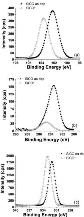
Figure6(a)shows the Si2p core level energy region origi-nating from Si atoms in the as deposited SiCO film. The Si2p spectrum exhibits one peak located at 102.2 eV assigned to Ox-Si-Cybonds.
12–14
Figure6(b)shows C1s core level energy regions of the SiCO film. The C1s spectrum exhibits two peaks, located at 283.5 and 285 eV. These C1s contributions are identified as C-Si and C-C bonds, respec-tively.12,15Figure 6(c) shows O1s core level energy regions of SiCO. The O1s spectrum exhibits only one peak, located at 532.5 eV and assigned to oxygen bonded to silicon in the SiCO environment.
After H2plasma exposure, the Si2p peak and C1s coming
from the SiCO bulk are not observed anymore. A shift to higher binding energy (104 eV) is detected, which is a char-acteristic of the Si-O4environment.
7
While the C1s spectrum shows a peak located at 285 eV assigned to C-C bonds coming from carbon contamination after air exposure. A shift of the O1s spectrum to 533.5 eV also confirms an important surface oxidation.
Notice that fluorine (not shown) is also detected on the XPS survey spectra after H2plasma, revealing the presence
of this species at the top surface probed by XPS. The fluo-rine detected in small amount (<3%) comes from the reactor walls.
Figure 7 shows that the pristine SiCO is composed of 37% silicon, 48% oxygen, and 15% carbon (13% C-Si and 2% C-C). After the hydrogen plasma process, the SiCO* film is oxidized (60% O and 40% Si) at the surface probed by XPS. Compared to the pristine film, the main difference after H2plasma exposure is the important surface oxidation.
Indeed, the SiCO* film is fully oxidized at the surface probed by XPS.
The trend observed on the SiCO* film is similar to the SiN film exposed to H2plasma.
7
Indeed, it has been reported that the SiN* film is fully oxidized at the surface probed by XPS after H2plasma (using similar plasma conditions).
7
FIG. 6. (a) Si2p, (b) C1s, and (c) O1s spectra recorded by XPS for the as deposited SiCO and SiCO* films.
FIG. 7. SiCO as deposited and SiCO* surface composition determined by XPS.
2. Film characterization by infrared spectroscopy
Figure 8shows the FTIR data of SiCO before and after H2plasma exposure in the 600–1700 cm−1 range (no peaks
are detected between 1700 and 4000 cm−1). The spectra are
characterized by different absorption bands assigned to Si-C stretching and Si-C bending vibration modes, centered at 800 and 1000 cm−1, respectively.14–16
Peaks located at 820 and 1040–1200 cm−1 are also
observed and assigned to Si-O-Si stretching in the longitudi-nal and transverse optical (LO–TO) modes, and the Si-O-Si asymmetric stretching in the TO mode,17respectively.
After H2 plasma exposure, the SiCO* T-FTIR spectrum
exhibits similar vibration bands as that of the pristine film (Fig.8). But, Si-C peak intensity decrease is observed which is in good agreement with XPS analyses previously described.
However, the MIR-FTIR spectrum of the as deposited film SiCO with or without H2 plasma exposure shows different
vibration bands (Fig.9). The main difference is the presence of a new peak of the Si-H stretching at 2210 cm−1 after H
2
exposure.18 This indicates higher H dose implanted in the SiCO* film after H2plasma exposure.
An additional wide vibration band of 3000–3700 cm−1 is
also detected after H2plasma exposure. This vibration band
is assigned to hydroxyl (-OH) bonds.18
In this study, we have shown that the SiCO* film modifi-cation depth can be controlled by plasma parameters like bias voltage. Indeed, with an increase of the bias voltage, a thicker SiCO* film damage thickness is measured after HF dip. This SiCO* film damage by H2plasma is characterized
by carbon depletion in the SiCO* film, oxidizing the film with important Si-H and Si-OH bonds’ formation.
In a previous study, we have demonstrated that the pres-ence of higher hydrogen concentration (Si-H and N-H bonds) in the silicon nitride film after H2plasma (SiN*) is
responsible for the higher etch rate.5,6 Our experimental results suggest different mechanisms.
Indeed, Fig. 10(a) shows that the Si-H peak intensity is the same when the SiCO film is exposed to H2plasma with a
bias voltage of 250 and 400 V. While in this case, the SiCO* film consumption by HF dip is estimated at 10 and 16 nm, respectively. Contrary to the study performed on the silicon nitride film, this result shows that Si-H bonds cannot explain, at the first order, the higher SiCO* film consumption. This carbon depletion is correlated with important SiOH bonds observed in Fig.10(a). The intensity of these SiOH bonds is all the more important that the bias voltage is high.
Therefore, this tends to indicate that this carbon depletion induced by H2 plasma (converting the SiCO film into
SiOxHy film) is responsible for the higher etch rate at the
first order when SiCO* is dipped in liquid phase HF.
C. Application to patterned wafer
The efficiency of the new etch method to remove the modified SiCO film on pattern structures has been evaluated using the stack described in Fig.1.
H2 plasma operating conditions have been adjusted to
target 13 nm silicon nitride film removal (targeting 30% over etch). After SiCO* film modification by H ions, 210 s 1% HF dip is performed to fully remove the modified layer.
After 25 nm silicon germanium epitaxial growth, the cross-sectional transmission electron microscopy (TEM) image (Fig. 11) shows that the silicon germanium interface presents a morphology compatible with correct epitaxial growth. After the epitaxial step, no foot formation is observed while the lateral spacer etching is estimated to be around 2.5 nm. Although in our experimental conditions, epitaxial growth is observed on top of the gate. This is explained by the nonselective long 1% HF dip process to the SiO2hard mask during the SiCO* removal step.
One solution to overcome this issue is to increase the ion energy and to reduce the HF dip time (as shown in Fig.12). But, the risk in this case is to induce silicon damage and epi-taxial growth defects. Indeed, using H2plasma conditions of
500 V and a 60 s 1% HF dip time, the SiO2hard mask is still
present protecting the top of the gate from epitaxial regrowth (Fig. 12). However, a rough surface is meanwhile observed
FIG. 8. T-FTIR spectra comparison of the SiCO film before and after H2
plasma performed in an ICP etch tool.
FIG. 9. MIR-FTIR spectra comparison of SiCO as deposited and after H2ion
which is a characteristic of silicon damage occurring during the H2modification step.
Finally, based on these results, the most appropriate approach would be to replace SiO2 or to add another hard
mask on top of SiO2 that is less sensitive to HF dip, for
instance, a silicon nitride hard mask.
IV. CONCLUSION
In this paper, we investigated SiCO film etching by a combination of H ion implantation performed in a conven-tional plasma etch tool (ICP) followed by a removal step of this modified layer using HF-based wet cleaning.
It has been shown that the SiCO*, modified by H2
plasma, can be fully removed on the blanket wafer by HF wet cleaning, while the pristine SiCO is barely etched.
A precise control of the SiCO* film damage thickness can be tuned by playing on the operating conditions like bias voltage.
It has been demonstrated that the H2 plasma exposure
leads to SiCO film oxidation with important Si-H and silanol group formation. The carbon depletion observed after H2
plasma (converting the SiCO film into the SiOxHy film) is
responsible for the higher etch rate at the first order when SiCO* is dipped in liquid phase HF.
Application on pattern revealed that this approach offers an interesting alternative way to conventional fluorocarbon-based chemistries. Indeed, after H2plasma followed HF dip,
the SiCO spacer can be etched without underneath film mod-ification, no foot formation, and less than 3 nm lateral SiCO consumption. A consumption of the SiO2 hard mask (not
compatible with the long HF dip time) has also been observed. Therefore, a trade-off has to be found between the bias voltage and the HF dip time. Otherwise, the replacement of the hard mask by a film less sensitive to the HF dip would be an interesting alternative.
1H. Niebojewski, C. Le Royer, Y. Morand, M. A. Jaud, O. Rozeau, E.
Dubois, and T. Poiroux, IEEE Euro SOI Conference, October 2013 (IEEE SOI, Monterey, 2013).
2
O. Weber et al., Symposium on VLSI Technology (2015), pp. T168–T169.
3F. Deprat et al.,Microelectron. Eng.167, A1 (2017). 4
V. Lu et al., International Conference on Solid State Devices and Materials (SSDM), Sapporo, September 2015 (SSDM, Sapporo, 2015). FIG. 10. MIR-FTIR (a) and T-FTIR (b) spectra comparison of SiCO films as
a function of bias voltage in the H2plasma.
FIG. 11. TEM view after SiCO spacer etching using H2plasma (400 V)
fol-lowed by a 210 s 1% HF dip and SiGe epitaxial growth.
FIG. 12. TEM view after SiCO spacer etching using H2 plasma (500 V)
followed by a 60 s HF dip 1% and SiGe epitaxial regrowth.
5N. Posseme, O. Pollet, and S. Barnola,Appl. Phys. Lett. 105, 051605
(2014).
6
V. Ah Leung, O. Pollet, N. Posseme, M. Garcia-Barros, N. Rochat, C. Guedj, G. Audoit, and S. Barnola,J. Vac. Sci. Technol. A35, 021408 (2017).
7
N. Posseme, V. Ah Leung, O. Pollet, C. Arvet, and M. Garcia-Barros,
J. Vac. Sci. Technol. A34, 061301 (2016).
8
O. Pollet, N. Posseme, V. Ah Leung, and M. Garcia-Barros,Solid State Phenom.255, 69 (2016).
9
D. Benoit et al., IEEE International Electron Devices Meeting (IEDM), December 2015 (IEDM, WA, 2015), pp. 8.6.1–8.6.4.
10
N. Rochat, A. Troussier, A. Hoang, and F. Vinet,Mater. Sci. Eng. C23, 99 (2003).
11N. Rochat, M. Olivier, A. Chabli, F. Conne, and G. Lefeuvre,Appl. Phys.
Lett.77, 2249 (2000).
12
N. Posseme, T. Chevolleau, O. Joubert, L. Vallier, and P. Mangiagalli,
J. Vac. Sci. Technol. B21, 2432 (2003).
13N. Posseme, T. Chevolleau, T. David, M. Darnon, O. Louveau, and O.
Joubert,J. Vac. Sci. Technol. B25, 1928 (2007).
14
H. Miyazaki,Jpn. J. Appl. Phys.47, 8287 (2008).
15
J. W. Yi, Y. H. Lee, and B. Farouk,Thin Solid Films326, 154 (1998).
16Y.-W. Koh, K.-P. Loh, L. Rong, A. T. S. Wee, L. Huang, and J. Sudijono,
J. Appl. Phys.93, 1241 (2003).
17
C. T. Kirk,Phys. Rev. B38, 1255 (1988).
18
M. Darnon, T. Chevolleau, T. David, N. Posseme, J. Ducote, C. Licitra, L. Vallier, O. Joubert, and J. Torres,J. Vac. Sci. Technol. B26, 1964 (2008).