HAL Id: lirmm-00838524
https://hal-lirmm.ccsd.cnrs.fr/lirmm-00838524
Submitted on 25 Jun 2013
HAL is a multi-disciplinary open access
archive for the deposit and dissemination of
sci-entific research documents, whether they are
pub-lished or not. The documents may come from
teaching and research institutions in France or
abroad, or from public or private research centers.
L’archive ouverte pluridisciplinaire HAL, est
destinée au dépôt et à la diffusion de documents
scientifiques de niveau recherche, publiés ou non,
émanant des établissements d’enseignement et de
recherche français ou étrangers, des laboratoires
publics ou privés.
A 3D IC BIST for pre-bond test of TSVs using Ring
Oscillators
Yassine Fkih, Pascal Vivet, Giorgio Di Natale, Marie-Lise Flottes, Bruno
Rouzeyre
To cite this version:
Yassine Fkih, Pascal Vivet, Giorgio Di Natale, Marie-Lise Flottes, Bruno Rouzeyre. A 3D IC BIST
for pre-bond test of TSVs using Ring Oscillators. NEWCAS: New Circuits and Systems, Jun 2013,
Paris, France. pp.001-004. �lirmm-00838524�
A 3D IC BIST for pre-bond test of TSVs
using Ring Oscillators
Yassine Fkih
(1,2), Pascal Vivet
(1)(1)CEA-Leti, MINATEC Campus,
F38054, Grenoble, France Email : [email protected]
Bruno Rouzeyre(2), Marie-lise Flottes(2)
, Giorgio Di Natale(2)
(2)LIRMM – Université Montpellier II/CNRS
Montpellier, France
Email: [email protected]
Abstract—3D stacked integrated circuits based on Through
Silicon Vias (TSV) are promising with their high performances and small form factor. However, these circuits present many test issues, especially for TSVs. In this paper we propose a novel Built-In-Self-Test (BIST) architecture for pre-bond testing of TSVs in 3D stacked integrated circuits. The main idea is to measure the variation of TSVs capacitances in order to detect defective TSVs. The BIST architecture is based on ring oscillators, frequencies of which depend on TSVs capacitances. The proposed BIST is integrated within the JTAG standard. This paper presents spice simulation results and logic synthesis results of the proposed TSV ring oscillator structure using a 65 nm CMOS technology, including 10 µm diameter TSV middle technology. Due to local process variations, the proposed test architecture is limited in accuracy; it detects only large capacitive faults on TSVs.
Key words: 3D IC, pre-bond test, TSV, ring oscillator, BIST, JTAG IEEE 1149.1 standard
I. INTRODUCTION
The stacking process of integrated circuits using TSVs (Through Silicon Via) is a promising technology that keeps the development of the integration more than Moore’s law, where TSVs enable to tightly integrate various dies in a 3D fashion. Regarding applications, 3D stacking allows a wide range of new SoC applications, such as heterogeneous stacking (Digital, Memory, RF, Mems); Interposers for multi-chip connection are becoming similar to a silicon board. The first envisaged 3D applications are mainly the WideIO DRAM 3D memory interface for high throughput and low power memory-on-logic stacking [1]. Nevertheless, 3D integrated circuits present many test challenges including the test at different levels of the fabrication process: pre-, mid-, and post- bond tests. Pre-bond test targets the individual dies at wafer level, by testing not only classical logic (digital logic, IOs, RAM, etc,) but also unbounded TSVs. Mid-bond test targets the test of partially assembled 3D stacks, whereas finally post-bond test targets the final circuit. It is generally admitted that a 3D test flow [2] should involve test procedures at all stacking levels of the 3D components including specific procedures for pre-bond TSV testing in order to provide Known Good Die before stacking.
In this context, pre-bond testing of TSVs is a real issue, due to the difficulty to get direct access to TSVs, which are not connected yet, using fine probe heads. So specific Design-for-Test structures for TSVs should allow to anticipate controllability and observability bottlenecks.
In this paper, we explore a test solution based on ring oscillators, which their oscillation frequencies depend on TSVs capacitances. This solution is based on the following principles: measurement of frequency variation instead of measurement of absolute charge or discharge time, implementation targeting full digital standard cell approach without the need of complex analog design. The proposed solution allows detecting misbehavior of the ring oscillator, which will be interpreted as a faulty TSV capacitance value. The technique allows pre-bond testing of TSVs while an exhaustive accurate TSV connection test will be performed after stacking using classical test approaches like boundary-scan [3]. Several defects can occur on TSVs, including: incomplete filling or presence of a micro-void in the TSV [2], and breaks in TSV metal [7]. These kinds of defects can cause modifications of the electrical characteristics of the TSV, especially on its capacitance [7]. Due to incomplete filling or micro-voids, the capacitance typically decreases.
This paper is organized as follows. In section II, we present the test architecture. In section III, we deal with the principle of TSV failure detection using ring oscillators, and some simulation analysis of the test infrastructure, In section IV, we present the BIST architecture at circuit level, and practical implementation on a system with numerous TSVs. In section V, we give conclusions and future work.
II. TEST ARCHITECTURE
Recently, 3D Design for Test architectures have been proposed such as [4], proposing a generic 3D test access mechanism using so called ‘test elevators’. There are also some recent efforts towards the creation of a 3D test standard [5]. But these design techniques do not address pre-bond test of TSVs. The aim of test of TSVs at pre-bond level is to detect faults early on the 3D fabrication flow. This is to control yield of Known Good Die before assembly including TSV test. At the same time, TSVs will be retested at
post-This work was funded thanks to the French national program 'programme d’Investissements d’Avenir, IRT Nanoelec' ANR-10-AIRT-05
bond, so the cost of pre-bond test should be reduced as much as possible, otherwise it will be useless to perform a TSV test at pre-bond level. The pre-bond test of TSVs can be seen from two points of view: the first one relies on the fact of using fine probe heads to establish direct contact with TSVs [6]. The second point of view is based on the indirect test, using dedicated test pads and an adapted test architecture [7, 8, 9]. Our proposed test architecture belongs to this approach. The underlying idea is that the TSVs' defects impact the delay of TSVs. Unlike related prior works, frequency variation is measured not charge or discharge time. Comparison is done between TSVs in the circuit not with a reference capacitor. Since, it is quite difficult or even impossible to measure these delays before the tier is bound, the principle is to connect the TSVs to embedded ring oscillators and to compare on-chip the frequencies of the oscillators. In fact a variation on the oscillation frequency means a variation on the TSV capacitance. The detection of the frequency variation is done by performing a comparison between frequencies of all ring oscillators in the circuit according to a test strategy.
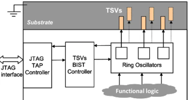
JTAG interface TSVs JTAG TAP Controller Ring Oscillators Functional logic TSVs BIST Controller Substrate JTAG interface TSVs JTAG TAP Controller Ring Oscillators Functional logic TSVs BIST Controller Substrate
Figure 1. TSV Test principle using BIST and ring oscillators
Figure (1) shows the test architecture. It is composed of two parts. The first part: the ring oscillators charging and discharging TSVs, frequencies of which depend on TSV capacitances, and on PVT variations. This point is further discussed in section III. The second part: the BIST controller that permits the control of the test, and the generation of result signatures that can be easily captured and shifted out through the JTAG interface. As shown in figure (1), TSVs are integrated in the silicon substrate, which is biased to the ground, and TSVs are not accessible from the external side. In pre-bond, before 3D stacking, only one side of the TSV can be accessed from the logic side which is used to perform the test. In Section III we present the first component of test architecture: the ring oscillators, and in section IV the second part: the BIST controller.
III. TSVFAILURE DETECTION USING RING OSCILLATORS
Several defects can occur on TSVs, including: incomplete filling or presence of a micro-void in the TSV [2], and breaks in TSV metal [7]. These kinds of defects can cause modifications of the electrical characteristics of the TSV, especially on its capacitance [7]. Due to incomplete filling or micro-voids, the capacitance typically decreases. Several defects can occur on TSVs, including: incomplete filling or presence of a micro-void in the TSV [2], and breaks in TSV metal [7]. These kinds of defects can cause modifications of the electrical characteristics of the TSV, especially on its
capacitance [7]. Due to incomplete filling or micro-voids, the capacitance typically decreases. Several defects can occur on TSVs, including: incomplete filling or presence of a micro-void in the TSV [2], and breaks in TSV metal [7]. These kinds of defects can cause modifications of the electrical characteristics of the TSV, especially on its capacitance [7]. Due to incomplete filling or micro-voids, the capacitance typically decreases.
In [10] an R, L, C model of the TSV is simplified to a pure capacitance model. We consider faulty TSVs to have smaller capacitance than non faulty ones. Therefore, a test method, that can be adopted, is to detect faulty TSVs by detecting the variation of its equivalent capacitance.
A. Presentation of TSVs Ringo Oscillators
Here we propose a test method that exploits the failure-induced capacitance modification of the TSVs; the idea is to implement a ring oscillator that charges and discharges TSVs, a variation in the propagation delay of the net connected to the failing TSV(s) induces a variation of the frequency of the ring oscillator, in case of failure. Since the TSV capacitance is rather large, compared to standard logic, it is expected to get a large enough effect of capacitance variation on frequency variation. The test structure is built from a ring of inverters, where one TSV is connected to the ring, and represent a load for the ring’s inverters (figure 2). The TSV is charged on a rising edge arising on the net of connection, and discharged on a falling edge. The more the TSV capacitance decreases, the more the ring oscillation period shortening is expected. The ring oscillator is composed of tri-state inverters: this allows to only enable the ring oscillator measurement for pre-bond test and to disconnect the ring oscillator structure from TSV functional paths in normal operation. The oscillator is initialized using a reset signal.
T S V T S V T S V
Figure 2. Test architecture of TSVs with one ring oscillator
However, in addition to the frequency variation expected in case of failing TSVs, the oscillation frequency of the proposed test structure depends also on other parameters such as the size and the number of inverters making up the ring oscillator, the number of TSVs connected to the test structure, and the operating conditions (process, voltage, temperature) which may strongly vary. Hereafter, we study the influence of process, voltage, and temperature (PVT) variations on the oscillation frequency of the ring oscillator and thus on its capacity to detect physical failures on TSVs.
B. Spice simulation results
Simulation-based experiments have been conducted using STMicroelectronics 65 nm technology, including a Leti TSV middle technology. The TSV characteristics are the following: a 10µm diameter, an 80µm depth (aspect ratio 1/8). An accurate spice RF model of the TSV can be found in [11].
For a TSV connected to the ground, its low frequency
equivalent capacitance is about 200 fF. This value is
considered as the reference value for a fault-free TSV in the sequel of this paper. As in [10], the TSV model used for spice simulations is a pure capacitance.
1) Impact of global variations of operating conditions In order to study the impact of process variations on oscillation frequency, we simulate the circuit shown on figure (2) in the typical case (typ / 1.0V / 25C), fast case (ff / 1.1V / -40C), and slow case (ss / 0.9V / 125C). For this, we varied the capacitance of the TSV from 200 fF down to 40 fF. And we studied the change on the parameter ∆F/F which measures frequency variation of the ring oscillator. ∆F/F equals to FFaulty_TSV – Fref(200fF) divided by Fref where Fref is the
reference frequency when the TSV is not faulty i.e. its capacitance equals to 200 fF.
Oscillation frequency in the typical, worst and best cases
0 500 1000 1500 2000 2500 20 40 60 80 100 120 140 160 180 200 C (fF) F (MHz) F (typ / 1,0V / 25C)) F(slow / 0,9V / 125C)) F(fast / 1,1V / -40C))
Figure 3. Oscillation frequency function of one single TSV capacitance for typical, fast, and slow operating conditions
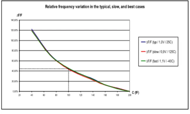
Simulation results in figure (3), shows, as expected, that process variation causes a very large modification on the frequency of the oscillator: the frequency is much higher in the fast corner case than in the slow corner one. As a consequence; a direct measurement of the frequency absolute value would be meaningless. Fortunately, process variation influences the oscillation frequency F but not the relative frequency variation ∆F/F as shown in figure (4).
Relative frequency variation in the typical, slow, and best cases
0,00% 20,00% 40,00% 60,00% 80,00% 100,00% 120,00% 140,00% 20 40 60 80 100 120 140 160 180 200C (fF) ∆F/F ∆F/F (typ / 1,0V / 25C) ∆F/F (slow / 0,9V / 125C) ∆F/F (fast / 1,1V / -40C)
Figure 4. Impact of operating condition variation on relative frequency variation
It can be observed that the ∆F/F parameter is constant for any global PVT operating conditions (worst, best, typical). By supposing that the circuit does not suffer from additional local process variability, differential measurement with ∆F/F allows to detect TSV capacitance variations, for any PVT conditions. For instance, as shown on figure (4), when the capacitance of one TSV decreases by 50%, ie equals to 100 fF, the relative
frequency variation equals to 43%. A test strategy based on relative frequency variation is better adapted, rather than direct measurement of frequency.
2) Impact of local variations of operating conditions In [12] local process variation is characterized using ring oscillators, the maximum local variation is 6,5%. The impact of this value is studied on the parameter ∆F/F (e.g. in figure 4, from 20% to 26.5% or 13.5%), which hide a capacitance variation of 22 fF (from 157 fF to 135 fF) i.e 11% of capacitance variation. As a result small capacitance variations on TSVs cannot be detected with the proposed test architecture because of local process variations, but large capacitive TSV defaults can be detected even with the presence of local process variations.
To deal with this limitation, one solution is to perform TSVs test per packet which are close geographically, so that the impact of local process variation will be negligible. C. TSV Defect Test Strategy
As of today, due to lack of accurate yield analysis and fault model for current TSVs, and due to the impact of local process variation, two test strategies have been elaborated: minimum approach, and average approach.
The first test strategy is proposed for simple fault models:
we assume that the slowest ring oscillator frequency Fmin is the
reference frequency (Fmin=Fref) which correspond to a properly
filled TSV, with a Cmax capacitance. We introduce the TTT
(TSV Test Threshold) parameter which is a programmable percentage that represents the selection threshold of ring
oscillators frequencies. We then calculate Fmax_TTT which
equals to Fmin + TTT% of Fmin. The two parameters Fmin and
Fmax_TTT define the selection interval of frequencies of ring
oscillators. Fmin Fmax_TTT Accept Reject Faverage +TTT%*Faverage Accept Reject -TTT%*Faverage Reject a) b) Fmin Fmax_TTT Accept Reject Faverage +TTT%*Faverage Accept Reject -TTT%*Faverage Reject a) b)
Figure 5. Defect detection test strategy based on statistical approach a) minimum approach, b) average approach
In figure (5.a), a statistical view of the comparison strategy
is given: the minimum frequency Fmin defines the left limit of
the selection interval and Fmax_TTT the right limit. Frequencies
between Fmin and Fmax_TTT are accepted, and frequencies above
Fmax_TTT are rejected, and corresponding TSVs considered as
faulty: due to bad copper filling or even worse in case of loss of Metal 1/TSV connection. The second test strategy is proposed to handle more accurate TSV fault models, where selection procedure is defined (figure 5.b) with computation of
the average frequency (Faverage) and a selection window
corresponding to the range [–TTT%*Faverage, + TTT%*Faverage].
The role of the BIST controller is to implement these two TSV test selection strategies and allow easy control for the user to choose the convenient one.
IV. BISTARCHITECTURE AT CIRCUIT LEVEL
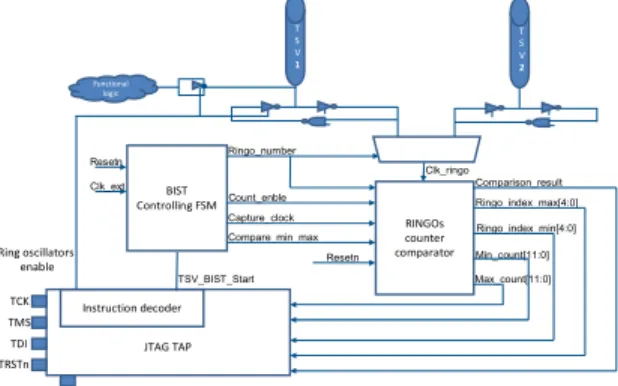
The BIST controlling FSM, shown in figure (6), selects one ring oscillator output at a time for Tcount ns. During this time, the counter comparator counts the number of clock cycles of the selected oscillator. Tcount is loaded from the JTAG interface and can be counted either by an external reference clock clk_ext, or by the JTAG clock tck. The selection between the 2 clocks is configured also through the JTAG interface. RINGOs counter comparator JTAG TAP Instruction decoder BIST Controlling FSM Min_count[11:0] Max_count[11:0] Ringo_index_min[4:0] Ringo_index_max[4:0] Resetn Clk_ringo Count_enble Capture_clock Ringo_number Resetn Clk_ext TSV_BIST_Start Compare_min_max Comparison_result Functional logic T S V 1 Ring oscillators enable TMS TDI TRSTn TDO T S V 2 TCK
Figure 6. BIST architecture integration within JTAG logic
Once all ring oscillators have been exercised, minimum and maximum numbers of clock cycles are stored. They correspond respectively to the slowest, and the fastest oscillators taken into considerations. Comparison step can then be started. Pass/fail comparison is done by comparing the minimum and maximum of the counted values: if the maximum counted value is bigger than TTT% of the minimum value then the result of test is fail, else pass. The BIST is integrated within the JTAG standard: it can be launched after shifting the adequate instruction code. Using the JTAG port, all BIST parameters are loaded including: test strategy (min/max or average), TTT factor, Tcount , and BIST clock selection. BIST results: comparison result, counted values and indexes are also captured and shifted out through the JTAG port at the end of the BIST.
We implemented the circuit shown in figure (6), and performed logic synthesis with STMicroelectronics 65 nm
standard cell libraries. Considered frequencies were: FJTAG_tck=
50 MHz and FBIST_clk_ext = 100MHz. The execution time of the
pass/fail BIST of 1000 TSVs was about 2 ms, with a digital accuracy of counting 800 rising edge per ring oscillator. Diagnose and debug instructions were added in order to return the number and index of faulty TSVs.
Component Area (µm2)
JTAG logic 5400 Boundary-scan cells 34600 BIST logic (pass/fail) 4000 BIST logic (debug/diagnostic) 5500 Ring oscillators 19800 Total DfT (pre-bond only) 34700 Total DfT (post-bond only) 40000 Total DfT (pre-bond & post-bond) 69300
Table.1: Area of the DfT architecture for 1000 TSVs
In order to compare our pre-bond TSV test architecture with standard boundary-scan approach that can be used for 3D TSV connection post-bond test, we have also evaluated the cost of boundary-scan cells controlled by the same JTAG logic. Areas of the different DfT components are presented in table 1. The area cost of proposed architecture for pre-bond test is slightly smaller than standard boundary-scan approach for post-bond test: ring oscillators area overhead is smaller than boundary-scan cells, while the area of the total BIST logic is negligible.
V. CONCLUSION AND FUTURE WORK
We have presented in this paper a test architecture, based on ring oscillators that are charging TSVs, to perform a pre-bond test of TSVs. The variation of capacitance of TSVs is detected by the variation of the frequency of ring oscillators. The test architecture is integrated in a built in self test (BIST) compliant with the JTAG standard. The digital controller of the BIST was designed to be flexible in order to take into consideration capacitive TSV default models and also to compensate PVT variations by the mean of a programmable test defect strategy. Next work is to investigate the possibility of integration, of ring oscillators as a small hard-macros placed in the area between TSVs i.e. in the unused area defined by the TSVs' pitch spacing, with respect to TSVs keep out zone.
REFERENCES
[1] WideIO JEDEC standard, see http://www.jedec.org/
[2] E.J. Marinissen and Y. Zorian, "Testing 3D chips containing through-silicon vias", in Proc. ITC, 2009, pp.1-11.
[3] "IEEE Standard Test Access Port and Boundary-Scan Architecture", IEEE Std 1149.1-2001.
[4] E.J Marinissen, J Verbree, M Konijnenburg " A structured and scalable test access architecture for TSV-based 3D stacked ICs", in proceedings of VTS 2010, pp. 269 – 274.
[5] IEEE 3D-Test Working Group (3DT-WG), see
http://grouper.ieee.org/groups/3Dtest/
[6] B. Noia and K. Chakrabarty, "Pre-bond probing of TSVs in 3D stacked ICs", in Proc. ITC, 2011, pp.1-10.
[7] Y. Lou, Z. Yan, F. Zhang, and P.D. Franzon, "Comparing Through-Silicon-Via (TSV) Void/Pinhole Defect Self-Test Methods", presented at J. Electronic Testing, 2012, pp.27-38.
[8] Yuan Chen, Cheng-Wen Wu, Ding-Ming Kwai "On-Chip TSV Testing for 3D IC before Bonding Using Sense Amplification", in proceedings of ATS’ 2009.
[9] Tsai M, Klooz A, Leonard A, Appel J, Franzon P, "Through silicon via (TSV) defect/pinhole self test circuit for 3D-IC", in proceedings of 3D’IC, 2009.
[10] Sergej Deutsch and Krishnendu Chakrabarty, "Non-Invasive Pre-Bond TSV Test Using Ring Oscillators and Multiple Voltage Levels", in Proc DATE’2013, pp 1065-1070
[11] M. Brocard et al, "Characterization and Modelling of Si-Substrate Noise Induced by RF Signal Propagating in TSV of 3D-IC Stack", ECTC 2012.
[12] F. Bruguier, P. Benoit, P. Maurine, and L. Torres, " A New Process Characterization Method for FPGAs based on Electromagnetic Analysis", FPL’ 2011, pp 20-23