HAL Id: cea-02340851
https://hal-cea.archives-ouvertes.fr/cea-02340851
Submitted on 31 Oct 2019HAL is a multi-disciplinary open access archive for the deposit and dissemination of sci-entific research documents, whether they are pub-lished or not. The documents may come from teaching and research institutions in France or abroad, or from public or private research centers.
L’archive ouverte pluridisciplinaire HAL, est destinée au dépôt et à la diffusion de documents scientifiques de niveau recherche, publiés ou non, émanant des établissements d’enseignement et de recherche français ou étrangers, des laboratoires publics ou privés.
The effect of electron and UV irradiation on graphene
single layer Raman spectra behaviour
I. Shchedrina, C. Corbel, O. Cavani, J.-P Renault
To cite this version:
I. Shchedrina, C. Corbel, O. Cavani, J.-P Renault. The effect of electron and UV irradiation on graphene single layer Raman spectra behaviour. Graphene 2017, Mar 2017, Barcelona, Spain. �cea-02340851�
Graphene2017
March 28-31, 2017 Barcelona (Spain)
The effect of electron and UV irradiation on
graphene single layer Raman spectra behaviour
I. Shchedrina1
C. Corbel1, O. Cavani1, J.-P. Renault2
1 LSI, Ecole Polytechnique, CEA, CNRS, Université
Paris-Saclay, 91128, Palaiseau, France
2 NIMBE, CEA Saclay, IRAMIS, 91191 Gif sur Ivette,
France
ShchedrinaIrina@gmail.com
Abstract
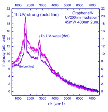
The reactivity and homogeneity of graphene surface, and, therefore its Raman spectra, are expected to be dependent on the quantity and type of structural defects that, as reported in literature, can be induced by various treatments, including irradiation [1-3]. Indeed, for UV irradiation, the evolution of the Raman spectra reveals a strong dependency on the irradiation conditions (light wavelength, electron energy, flux, irradiation dose). Similar behavior was found by other authors [1, 4] using different irradiation conditions.
The present work is focused on surface properties changes, induced by irradiation in graphene materials and investigated by Raman and photoluminescence (PL) spectra at the micro scale. The aim is to investigate more specifically the evolution of the Raman and PL spectra before and after different types of irradiation and their correlation. Irradiation tests are performed in dry conditions for graphene single layer deposited on Ni substrate and, to compare, for highly oriented pyrolytic graphite (HOPG).
As illustrated on Fig.1 for a graphene monolayer on Ni after 1h UV irradiation, the spectra evolve as the concentration of electron irradiation induced defects compared to the native defects increase, moreover the Raman and the PL spectra
vary independently as the UV flux used for the 1h irradiation increases.
References
[1] Teweldebrhan D. et al. Appl. Phys. Lett., 94,013101–013103, (2009) [2] Kotakoski J. et al. PRL 106, 105505
(2011)
[3] Giannazzo F. et al. Nanoscale Research Letters (2011)
[4] Pimenta M ;A. et al. Phys. Chem. Chem. Phys., 9, 1276-1290 (2007) Figures 1000 2000 3000 4000 5000 6000 7000 0 2 4 6 8 10 12 14 16 18 20 22 1000 2000 3000 4000 5000 6000 7000 0 2 4 6 8 10 12 14 16 18 20 22 Before(line) 1h UV-weak(dot) 1h UV-strong (bold line)
nk (cm-1) In te n si ty (a rb . u n it ) Graphene/Ni UV200nm Irradiation 45mW 488nm 2µm
Figure 1: Raman and Photoluminescence
spectra (spot 2µm, laser wavelength 488nm, intensity 45mW) in single layer Graphene/Ni before and after 1 hour of ultra-violet (200nm) irradiation at low and high flux