HAL Id: hal-01138682
https://hal.archives-ouvertes.fr/hal-01138682
Submitted on 3 Apr 2017
HAL is a multi-disciplinary open access
archive for the deposit and dissemination of
sci-entific research documents, whether they are
pub-lished or not. The documents may come from
teaching and research institutions in France or
abroad, or from public or private research centers.
L’archive ouverte pluridisciplinaire HAL, est
destinée au dépôt et à la diffusion de documents
scientifiques de niveau recherche, publiés ou non,
émanant des établissements d’enseignement et de
recherche français ou étrangers, des laboratoires
publics ou privés.
Highly Efficient Infrared Quantum Cutting in Tb3+–
Yb3+ Codoped Silicon Oxynitride for Solar Cell
Applications
Yong-Tao An, Christophe Labbé, Julien Cardin, Magali Morales, Fabrice
Gourbilleau
To cite this version:
Yong-Tao An, Christophe Labbé, Julien Cardin, Magali Morales, Fabrice Gourbilleau. Highly
Effi-cient Infrared Quantum Cutting in Tb3+– Yb3+ Codoped Silicon Oxynitride for Solar Cell
Appli-cations. Advanced Optical Materials, Wiley, 2013, 1 (11), pp.855-862. �10.1002/adom.201300186�.
�hal-01138682�
FULL P
APER
www.MaterialsViews.com
Highly Effi cient Infrared Quantum Cutting in Tb
3+
−Yb
3+
Codoped Silicon Oxynitride for Solar Cell Applications
Yong-Tao An , Christophe Labbé ,* Julien Cardin , Magali Morales ,
and Fabrice Gourbilleau
1. Introduction
Among the different approaches to improve the solar cells effi ciency, the quantum cutting (QC) is one of the interesting ways proposed since the thermalization effect of the electrons is limited for the energetic photons. [ 1–3 ] Placed on top of a solar
cell, a QC layer consists in dividing the absorbed UV-Visible photon energy to emit two IR photons absorbed by the classical Si solar cell below. This down-conversion (DC) process leads to a quantum effi ciency (η QE ) higher than 100% as theoretically
predicted by Dexter et al. [ 4 ] and experimentally seen by different
authors on Pr 3+ -, Tm 3+ -, or Gd 3+ -doped host matrices. [ 5 ] . Almost
15 years ago, a high η QE was achieved close to 200% by Wegh
et al. [ 6 ] on a LiGdF
4 :Eu 3+ –Gd 3+ phosphor system. This result
has relaunched the research activity on the development of effi -cient QC layers. [ 2,7,8 ] Another system based on double co-doping
Er 3+ –Gd 3+ –Tb 3+ was studied in such a matrix, [ 9 ] but a system
associating a donor to Yb 3+ ion seems
to be more promising. Indeed, the Yb 3+
ion has a single excited state, reducing the harmful effect of up-conversion and harvesting the energy corresponding to a photon emission of 1 μm wavelength, just above the gap of c-Si thus limiting the thermalization. [ 10 ]
In this regard, the scientifi c community makes great effort to enhance the η QE of
Yb 3+ doped materials. The fi rst report on
effi cient DC material containing Yb 3+ ions
was on Tb 3+ -Yb 3+ system in phosphor
matrix with the achievement of a 188% internal η QE . [ 11 ] This has been followed
by several studies on the same system in different host matrices such as borate (η QE = 196% and 152%), [ 12,13 ] hafnia glass
ceramic (η QE = 138%), [ 14 ] oxyfl uoride glass
(η QE = 120% and 166%). [ 15,16 ] High η QE
were also demonstrated in system associating Yb 3+ with other
absorber-donor rare earth ions such as Ce 3+ (η
QE = 174%) in a
borate glasses, [ 17 ] Pr 3+ (η
QE = 197%) in a fl uoride, [ 18 ] and Er 3+
ion (η QE = 196–199%) in a glass ceramic and a bromide matrix
respectively. [ 19,20 ] Unfortunately, most of these rare earth-doped
hosts are not easily compatible with the fabrication process of conventional crystalline silicon solar cells. Consequently, the gain achieved in terms of photon is lost by the cost required to adapt the fabrication line and/or to design a new solar cell structure. This is the reason why some investigations are now focusing on silicon integration: Zn 2 SiO 4 :Tb 3+−Yb 3+ , [ 21 ] silicon
nanocrystals, [ 22 ] Er 3+ in SiO 2 . [ 23 ]
In order to obtain both a host environment based on silicon to offer an industrial compatibility and a very high down-conversion η QE , we propose to investigate a silicon oxynitride
matrix codoped with Tb 3+ –Yb 3+ system. To perform this study,
the photoluminescence (PL), PL excitation (PLE) as well as the decay lifetimes were investigated as a function of the Yb 3+
concentration. The latter allowed us to calculate the η QE which
has been enhanced up to almost 197% in such host matrix. By considering the non-radiative losses, a rough correction, never taken into account in previous similar studies, gives a η QE of
183%. Our work demonstrates the feasibility of a high η QE
down-converter thin fi lm easily deposited on a common solar cell to improve its external quantum effi ciency. This additional external quantum effi ciency due to this DC effect is evaluated to almost 2%.
Y.-T. An, Dr. C. Labbé, Dr. J. Cardin, Dr. M. Morales, Dr. F. Gourbilleau
Centre de Recherche sur les Ions les Matériaux et la Photonique (CIMAP) UMR 6252 CNRS/CEA/Ensicaen/UCBN 6 Boulevard Maréchal Juin, Cedex 4 , 14050 Caen , France
E-mail: [email protected]
DOI: 10.1002/adom.201300186
A high effi ciency infrared quantum cutting effect in a Tb 3+ –Yb 3+ codoped
silicon oxynitride system is demonstrated. The thin fi lms are deposited on Si substrates by reactive magnetron co-sputtering of a Si target topped with Tb 4 O 7 and Yb 2 O 3 chips under pure nitrogen plasma. The photoluminescence
dynamics are investigated, revealing a quantum effi ciency of this system at 980 nm up to 197% for the higher Yb 3+ concentration. Thus, via a
coopera-tive transfer mechanism between Tb 3+ and Yb 3+ , an absorbed UV–visible
photon gives rise to almost two emitted IR photons. Such a down-conversion effect is demonstrated upon indirect excitation of energy donors, via defect states in the host matrix. These down-converter fi lms could be directly and easily integrated on top of the Si-based solar cell to improve the photoelectric conversion effi ciency at a lower cost. An evaluation of the additional external quantum effi ciency is deduced from this optical system and found to be almost 2%.
2 wileyonlinelibrary.com © 2013 WILEY-VCH Verlag GmbH & Co. KGaA, Weinheim
FULL P
APER
FULL P
APER
FULL P
APER
www.MaterialsViews.com2. Results and Discussion
2.1. Samples
The thicknesses of the deposited fi lms were measured 201 to 245 nm (±10 nm). The refractive index is constant of about 1.73. The concentrations of different elements deduced from the RBS experiments are displayed on the Table 1 .
As shown, the silicon content is almost constant of about 30 at% whereas the nitrogen content tends to decrease with the Yb 3+ concentration in favor of the oxygen element. The amount
of oxygen contained only in the Tb 4 O 7 and Yb 2 O 3 chips could
contribute to the formation of SiO 2 phase detected by the
pres-ence of Si-O bond in FTIR spectrum as previously reported. [ 24 ]
The refractive index measured is consequently the signature of a composite layer containing SiO 2 (n = 1.55) and Si 3 N 4 (n = 2.00)
phases. Moreover, the lower 1.73 value could also be ascribed to the excess of nitrogen incorporated with respect to the stoi-chiometric Si 3 N 4 matrix. Indeed the nitrogen excess (N excess ),
responsible for the deviation from a perfect SiO 2 +Si 3 N 4 mixture
is calculated with help of the equation ( 1) :
Nexcess
( )
/ 4 / 3( )
2 / 3/ 3( )
7 / 6[ ]
Tb( )
1/ 4[ ]
Yb[ ]
Tb[ ]
Yb[ ]
Si[ ]
Si[ ]
N[ ]
O[ ]
N[ ]
O = 4 / 3 −(
7 / 6 Si +[ ]
Tb + (1) where the term [element] represents the atomic concentra-tion (at%) of the aforesaid element. [ 25 ] On the basis of Kistneret al. [ 26 ] study, this excess of nitrogen explains the value of 1.73
measured. So our deposited thin fi lm is a nitrogen-rich silicon oxynitride (NRSON). Note that even if the number of Tb 4 O 7
chips is constant during the deposition run, the Tb 3+
concen-tration is multiplied by 2.5 with the increasing number of the Yb 2 O 3 chips.
2.2. Photoluminescence
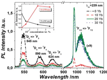
The PL spectrum of the Tb 3+ monodoped sample is displayed
in Figure 1 with a 239 nm excitation wavelength, corresponding to the best PL signal taking account our experimental set up response.
In the visible range, the peaks of the Tb 3+ at 545, 590 and
624 nm were identifi ed as the transitions 5 D
4→ 7 F j (j = 5, 4, 3)
respectively. In our previous study, [ 24 ] a non-resonant excitation
wavelength with the Tb 3+ ion at 325 nm, allow us to see also the
transition at 490 nm, like Jeong et al. with the same matrix, [ 27 ]
corresponding to the transition 5 D
4→ 7 F 6 , hidden by the
second-order grating with a 239 nm excitation wavelength. These four transitions are depicted in Figure 2 .
On the Figure 1 , when a small content of Yb 3+ ions is
added (10Yb curve), we note a remarkable decreasing Tb 3+
PL intensity and concomitantly in the IR range emerging two typical Yb 3+ peaks located at 976 and 1026 nm coming from 2 F
5/2→ 2 F 7/2 transition. The variation of these visible and IR
PL peaks intensities versus the Yb 3+ concentration are shown
in the inset of Figure 1 . The PL intensity of the Tb 3+ ion at
545 nm decreases, with the Yb 3+ concentration, while that of
Yb 3+ PL increases. This opposite behavior is the sign of
coop-erative DC energy transfer (ET) as shown on the Figure 2 . The
5 D
4 – 7 F 6 Tb 3+ energy transition (490 nm ≈ 2.53 eV) is divided
Table 1. Atomic composition measured by RBS technique an d the
excess of nitrogen (N excess ) deduced.
Sample name based on the Yb 2 O 3 chip number Si [at%] N [at%] O [at%] N excess Tb [at%] Yb [at%] 0Yb 32.98 46.00 20.28 14.90 0.74 0 10Yb 31.53 34.11 32.54 12.23 1.34 0.48 20Yb 30.45 38.28 27.46 12.90 1.84 1.97 30Yb 28.89 26.06 39.68 9.73 1.86 3.51
Figure 1. PL spectra under 239 nm excitation wavelength as a function of
Yb 3+ concentration. In inset, the variation of the Tb 3+ and Yb 3+ PL
intensi-ties with the Yb 3+ concentration. Note that each Yb 3+ intensity is
multi-plied by a factor of 9 for a best readability.
Figure 2. Scheme of the Tb 3+ and Yb 3+ energy diagram depicting the QC
effect. Note that in this diagram we have supposed for the legibility that
the top of the valence band (E v ) is at the same energy than the rare earths’
FULL P
APER
FULL P
APER
FULL P
APER
www.MaterialsViews.com transitions 5 D4→ 7 F j (j = 5, 4, 3) respectively (Figure 2 ). In our
previous study without Yb doping, [ 24 ] we mentioned two energy
transfer mechanisms producing these four transitions coming from the 5 D
4 level of the Tb 3+ ion: (i) one coming from the
car-riers across the optical gap into the extended states-carcar-riers that could be captured directly by Tb 3+ related states, (ii) the second
when excitation energy is lower than the gap, carriers trapped in the band tail states can transfer energy to Tb 3+ ions. So with
the 488 nm (and also 457 nm and 476 nm not shown) excita-tion wavelength, which is non resonant with the Yb 3+ ion, the
last mechanism is involved, and gives a signifi cant Yb 3+ PL
intensity with the help of a DC effect. The best PL intensity is again obtained for the 20Yb sample.
2.3. Photoluminescence Excitation
To investigate in more details the excitation range of the Tb 3+
ion to get ET towards Yb 3+ , we perform the PLE spectra of the
samples with and without Yb 3+ ions normalized to the
thick-ness ( Figure 4 ).
The PLE measurements are carried out by setting the detec-tion at 545 nm attributed to the 5 D
4→ 7 F 5 transition of Tb 3+ , also
including the band tail. The PLE spectra range is extended from about 250 to 550 nm (≈2.2–5.0 eV), corresponding to the solar spectra range available for the DC effect. [ 1 ] The PLE intensities
behaviors following the lowering of the Tb 3+ PL intensity with
the Yb 3+ content attest that the transfer mechanism involved in
this system is effi cient in a wide range of wavelengths. The PLE spectra comprise three peaks centered at almost 3.8 eV, 4.3 eV, and 4.8 eV. These three peaks are also identifi ed in a sample without any rare earth (not shown) respectively centered at 3.3 eV, 3.8 eV, and 4.3 eV. The fi rst peak at 3.3e V is identifi ed as a nitrogen defect state (N 4 + ). [ 34 ] The second at 3.8 eV with a very
broad band (almost 1.5 eV width) is linked to the band tail, [ 35 ]
while the third one at 4.3 eV is due to the gap of the NRSON host matrix. Indeed the refractive index of the undoped sample is found to be 1.80 corresponding to a tauc gap of 4.3 eV based into two IR photons coming from two 2 F
5/2 – 2 F 7/2 Yb 3+ energy
transitions (980 nm ≈ 1.26 eV). [ 11,28 ] We also observe a
satura-tion and a slight decrease of the Yb 3+ PL intensity for the 30Yb
curve, when we almost have one Tb 3+ ion (1.86 at%) for two
Yb 3+ ions (3.51 at%) (see Table 1 ). This could be the expression
of the usual quenching effect observed for high concentration corresponding to a migration between the Yb 3+ ions into
non-radiative defects. But the self-quenching effect is ruled out here because it has been observed for system containing more than 10 at% concentration. [ 29,30 ] So this saturation could be explained
by the beginning of the formation of Yb 3+ clusters due to the
annealing of the samples at 700 °C, reducing de facto the active numbers of Yb 3+ ions. [ 31 ]
One may argue that, depending on the used host matrix, the 239 nm excitation wavelength (5.2 eV) could induce charge transfer energy on the Yb ion (Yb 3+→Yb 2+ ) and thus directly
excite the Yb 3+ ion without sensitizing the Tb 3+ . [ 32 ] To avoid this
drawback, we have excited the three Yb 3+ samples at 488 nm
which is clearly non resonant with the Yb 3+ ion, but resonant
with the Tb 3+ ion. [ 21,29 ]
The Figure 3 depicts clearly the Yb 3+ PL spectra in the IR
range suggesting an ET via the Tb 3+ ion is possible. The visible
range shows this time a broad band of almost 200 nm width and centered at 600 nm. This broad emission band is attributed to the band tail states of the matrix. [ 24,27,33 ] Indeed this band
tail comes from localized states associated with defects such as dangling bonds in the host matrix. Its PL spectrum is strongly blue-shifted with the decrease of the excitation wavelength (see Figure S1) due to the occupancy of the density of states. This visible band fi nally disappear when we use an excitation (239 nm ≈ 5.2 eV) higher to the band gap (4.8 eV), [ 24 ] due to
the trapping of the electron (Figure 1 and drawing in Figure 2 ). This effect is also seen by Kistner et al. [ 26 ] but in their case the
excitation wavelength is constant while the gap changes with the composition.
We also distinguish on Figure 3 a weak PL intensity of the Tb 3+ peaks at 545, 590, and 624 nm identifi ed as the Figure 3. PL spectra of the codoped Tb 3+−Yb 3+ samples excited at 488 nm
wavelength. Note that each the Yb 3+ intensity is multiplied by a factor of
9 for a best readability.
Figure 4. PLE spectra detected at a 545 nm wavelength corresponding
to the 5 D
4 wileyonlinelibrary.com © 2013 WILEY-VCH Verlag GmbH & Co. KGaA, Weinheim
FULL P
APER
FULL P
APER
FULL P
APER
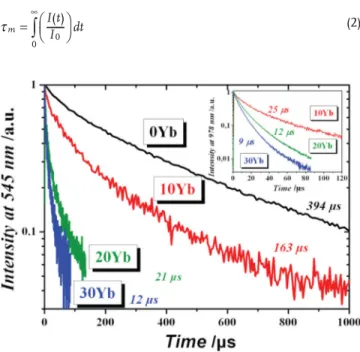
www.MaterialsViews.comwhere I(t) is the decay intensity and I 0 the maximum of the
I(t). [ 39 ] The values of the different samples are presented on
Figure 5 . The τ m of the Tb 3+ falls down drastically with the
increase of the Yb 3+ concentrations showing a reduction by a
factor of more than 30. Such an evolution with the Yb 3+
con-centration was also observed in previous studies, [ 3,13,15,16,21,29,40 ]
but in a lower proportion of a factor 4 at maximum whatever the Yb 3+ concentration. The decrease was identifi ed as the
con-sequence of the cooperative ET from one Tb 3+ to two Yb 3+ ions
acting as quantum cutting mechanism, and the factor 30 pre-suppose a very high effi ciency transfer.
2.5. Quantum Effi ciency
To quantify such cooperative ET, we calculate the energy transfer effi ciency (η ETE ) at 545 nm ( 5 D 4→ 7 F 5 ) described in the
formula ( 3) : 1 ETETT Tb Yb Tb η = −1 ττ− (3)
where τ Tb-Yb and τ Tb are the decay times of the Tb 3+ with and
without Yb 3+ , respectively. Thus the quantum effi ciency (η QE )
usually defi ned as the ratio between the total number of emitted photons and the total number of absorbed photons, is described by the formula ( 4) :
2 2 Q Tb ETE Tb Yb Tb ηQE ηηTb
(
(
11 ηETE)
222ηηETE= −ττ− (4) assuming that the quantum effi ciency of Tb 3+ is 1. [ 6,11 ]The Figure 6 shows the η QE of the transfer according to
the Yb 3+ concentration. To calculate the η
QE , it is always
sup-posed implicitly that τ Tb is constant in order to compare the
different Yb 3+ concentrations. During the increase of the Yb 3+
concentration, we note an increase of the Tb 3+ content by a
factor of 2.5, from 0.74 at% to 1.86 at%, mentioned previ-ously in the Table 1 , although the number of the Tb 3+ chips
is kept constant during the deposition process. This increase of the Tb 3+ concentration could contribute to a variation of
its own lifetime by two different effects (cross relaxation or to the average results reported by Kistner et al. [ 26 ] and Wang et
al. [ 36 ] The four rare earth-doped samples in this study have a
refractive index of 1.73 resulting in a slightly higher gap which explains the energy position shift of almost 0.5 eV of their three peaks compared to their undoped counterparts. Therefore the three peaks at 3.8 eV, 4.3 eV, and 4.8 eV of the doped samples on the Figure 4 , are attributed also to the nitrogen defect state (N 4 + ), band tail and band gap respectively, and are represented
schematically in the diagram of Figure 2 . The excitation of Tb 3+
in such thin fi lms was previously studied and has proved the involvement of these energy states in the excitation mecha-nism, confi rming our results of the PLE spectra. [ 27,35 ] Thus the
excitation of the Tb 3+ ions in a large spectral range in order to
obtain a DC effect with an Yb 3+ ion is possible, upon indirect
excitation of energy donors, via defect states in the NRSON host matrix.
2.4. Time-Resolved Photoluminescence
Figure 5 depicts the decay times of the Tb 3+ at 545 nm
( 5 D
4→ 7 F 5 ) under 239 nm excitation wavelength with different
concentrations of Yb 3+ .
The lifetime curves present a biexponential decay. For example, the Yb 3+ -free sample displays fast (151 μs) and slow
(627 μs) components. Note that the lifetime linked to the band tail is a nanosecond time scale and is not detectable here. [ 36,37 ]
The slow decay value is comparable to that obtained in similar matrix with a Tb 3+ concentration four times lower. [ 27 ] These
two decays could correspond to the Tb 3+ ions linked to the Tb
cluster (fast component) and the “isolated” Tb ions (slow com-ponent). [ 38 ] To overcome such non exponential decays, a mean
decay time (τ m ) is calculated by the formula ( 2) : I t I dt m ( )t 0 0
∫
τ = ⎛⎝⎛⎛⎛⎛⎝⎝⎛⎛⎛⎛ ⎞⎠⎞⎞⎞⎞⎠⎠⎞⎞⎞⎞ ∞ (2)Figure 5. Tb 3+ decay times at 545 nm under a 239 nm excitation
wave-length with different concentrations of Yb 3+ . In inset: Yb 3+ decay times at
980 nm under a 239 nm excitation wavelength with different
concentra-tions of Yb 3+ .
Figure 6. Tb 3+ decay times at 545 nm under a 239 nm excitation
FULL P
APER
FULL P
APER
FULL P
APER
www.MaterialsViews.comtime (τ Yb = 25 μs) of the lower Yb 3+ concentration sample, the
non-radiative rate is described by the equation ( 7) : 1 1 1
NR Yb Yb
τNR=τ −τ′
(7)
where τYb′ is the decay time of the higher Yb 3+ concentration
sample (9 μs). The τTb Yb′ − is found to be almost 66 μs, then
giving a new quantum effi ciency ηQE′ of 183%, compared to
the 197% found, without taking into account these NR losses. Of course the component 1/τ NR is not exactly the same for Tb 3+
and Yb 3+ , but this method could give a rapid proportion of the
overestimated η QE , never made in the literature.
3. Additional External Quantum Effi ciency
Evaluation
The additional external quantum effi ciency (ηEQEadd) induced by
this DC layer has been estimated. An external quantum effi -ciency of a conventional solar cell ( sc ) with a DC fi lm is noted
EQEwith
η . To extract the additional external quantum effi ciency cause by the DC layer, we have to take into account a possible loss of the external quantum effi ciency (ηEQEloss) of the sc due to
its partial occultation by this converting frequency layer. Then the additional external quantum effi ciency (ηEQEadd) can thus be
obtained in according to the equation ( 8) :
EQEadd EQEwith EQEloss
η
EQEaddη
η
EQEwith−
η
(8) The ηEQEwith is defi ned by the ratio between the charge carriers
generated by the sc and the incident photons on the sc in the DC wavelength range (φ sun ), i.e. ,between 250 nm and 550 nm as
mentioned above. [ 1 ] The effi ciency of the sc for a corresponding
wavelength λ is called (( λ). Thus the charge carriers generated by the sc are obtained by the product of the ηsc980 and the
inci-dent photons fl ux on the sc at 980 nm wavelength coming from the conversion performed by the DC layer (φ’ sc ). The ηEQEwithis
well defi ned by the equation ( 9) :
EQEwith sc980 sc sun ηEQEwith η φφ ′ (9) To separate each effi ciency, corresponding at each step of the conversion, we defi ne Δφ DC representing the absorbed photon
fl ux inside the DC layer. After the DC process, φ′ DC describes
the emitted photon fl ux at the 980 nm wavelength inside the DC layer ( Figure 7 ).
Therefore the ηEQEwith can be rewritten by the equations ( 10)
and ( 11) : EQEwith sc980 DC sun DC DC sc DC ηEQEwith η ⎝⎛⎛⎛φφ ⎠⎞⎞⎞ ⎛⎝⎜⎛⎛⎝⎝φφ ⎞⎞⎞⎠⎟⎠⎠⎛⎛⎝⎝⎛⎝⎜φφ ⎞⎠⎟⎞⎞⎠⎠ ′ φ ′ ⎞ ⎛ ′ (10) EQE . . with
sc980 absDC convDC 980 extr980xx ac
ηEQEwith η .η ηabsDC. → .η
(11) where, ηabsDC, convDC 980 η → , and extr980xx ac
η are the different effi ciencies linked respectively to the different terms of the equation ( 10) . migration) and affect the comparison. In the fi rst effect, the
known cross relaxation is defi ned by ( 5 D
3→ 5 D 4 )/( 7 F 6→ 7 F 0 )
transitions, which contributes to extend the 5 D
4
experi-mental lifetime and consequently underestimates the η QE
obtained. [ 41 ] On the contrary, the self-quenching process,
caused by the migration of the excitation energy of the Tb 3+
to non-radiative defects could reduce the τ Tb ( 5 D 4 ) and
over-estimate the η QE . But the decrease of the intensity linked to
the migration is usually observed for very high concentra-tion of Tb 3+ , which has not been studied in this work. [ 42 ] So
the τ Tb ( 5 D 4 ) is not affected by Tb 3+ concentration used. On
Figure 6 , we observe an increasing of the η QE following by
a plateau at 197%. This plateau is due to weak variation of the τ Tb-Yb values (21 μs to 12 μs) compare to the τ Tb (394 μs).
Note that the behaviors of the variation with the Yb 3+
con-centration of the fast and slow Tb 3+ decay times are the same
as the τ m , which represents an average of these two
compo-nents. So for the fast and slow components, the η QE limits
are almost the same, 198% and 195% respectively. This means that almost two Yb 3+ ions are excited for one excited
Tb 3+ ion attesting a highly effi cient quantum cutting
mecha-nism. This limit has been approached for a Tb 3+ -Yb 3+ system
in phosphor matrix (η QE = 188%) [ 11 ] or borate (η QE = 196%) [ 12 ]
and with other rare earth with Yb 3+ like Pr 3+ (η
QE = 197%) [ 18 ] ,
or Er 3+ (η
QE = 196–199%). [ 19,20 ]
Usually, the η QE calculations suppose that the decrease of the
Tb 3+ lifetime with the Yb 3+ content is completely attributed to
the ET. [ 13 ] But the increase of the Yb 3+ concentration could
intro-duce some non-radiative (NR) losses, by inclusion of defects or impurities, contributing to the fall of the decay time and over-estimate the η QE . To investigate this point, we have measured
the Yb 3+ lifetime at 980 nm wavelength (inset Figure 5 ). The
Yb 3+ decay time is reduced from 25 μs to 9 μs with the increase
of the concentration, revealing the NR losses, because the self-quenching effect is not expected as mentioned above. [ 29 ] In spite
of the Yb 3+ lifetime diminution, we observe that its PL intensity
is constantly increasing (inset Figure 1 ) with the Yb content. This is due to the growing number of excited Yb 3+ ions and the
effi cient ET that counterbalances this weak decrease linked to the NR losses. To take into account this effect, and see how this decrease could affect the η QE , we have estimated the
nonradia-tive rate (1/τ NR ) considering that τ Tb is affected by the ET and
NR losses and can be described by the following equation ( 5) : 1 1 1 1 Tb Yb Tb ET NR τTb Yb=τ +τET+τ (5) So we can defi ne in equation ( 6) , a new lifetime by τTb-Yb′ to
calculate the new quantum effi ciency ηQE′ taking into account
the NR part. 1 1 1 1 1 Tb Yb Tb Yb NR Tb ET τ′ − =τTb Yb−τ =τTb+τ (6) To roughly estimate the non-radiative rate (1/τ NR ) for the
Tb 3+ , we use the Yb 3+ decay measurements considering that the
lowering of the quality approximately affects the decay times of the rare earth in the same proportion (see inset Figure 5 ). Based on the fact that we assume there are no NR losses for the decay
6 wileyonlinelibrary.com © 2013 WILEY-VCH Verlag GmbH & Co. KGaA, Weinheim
FULL P
APER
FULL P
APER
FULL P
APER
www.MaterialsViews.com 10 12 ph s −1 m −2 . Consequently, the absDC η is equal to 14% of the incident solar photons, on the DC range.iii. The effi ciency ηconvDC 980→
The energy transfer demonstrated above between the host matrix and the Tb 3+ ion (η
matrix→Tb ) is supposed here
equal to 100%. It means that all the absorbed photons by the host matrix are transferred to the Tb 3+ ion and contributed
to the DC conversion process. Note that the photon fl ux is less than the common densities of the rare earth ions usu-ally used and consequently the effi ciency is not limited by an eventual saturation. So the ηconvDC 980→ effi ciency is defi ned
by the product of (η matrix→Tb = 100%) and the ηQE′ found
in Section 2.5 at 183% taking account the NR losses, i.e., a
convDC 980
η → equal to 183%.
iv. The effi ciency ηextr980xx ac
The PL emission is omnidirectional. So, in this part, we have to take into account the extraction of the down-con-verted low-energy photons in the sc which are confi ned in a layered media formed by the DC layer stack on the sc . [ 7 ]
Based on a transfer matrix formalism and electric dipole source terms, [ 44 ] a method of modeling light emission in
lay-ered media has been developed. This method leads us to the distribution modeling of emitted intensities versus emission angle in each considered medium ( Figure 9 a) and versus wavelength i.e. around 980 nm for the Yb 3+ ion in this case.
We consider an average DC layer thickness of 225 nm, with refractive index describe by a new amorphous model. [ 45 ] The
emission of Yb 3+ ions was modelized by a Lorentzian
func-tion centered at 980nm and with a FWHM of 50nm. So we obtained the PL spectra by the integration over emission angles in DC and sc materials ( Figure 9 b). This numerical calculation shows that the effi ciency ηextr980xx ac is equal to 30%.
Therefore the external quantum effi ciency induced by the DC layer (ηEQEwith) is found to be 2.53%, using the equation ( 12) .
. .
32.9% 14% 183% 30% 2.53%
EQEwith sc980 absDC convDC 980 extr980xx ac
ηEQEwith η .η ηabsDC. .η
=32.9%× ×183%× =
→
(12) To calculate the loss due to the occultation by DC layer (ηEQEloss)
of 14% of the incident energy on the sc , we assume no DC effect (ηconvDC 980→ =100%)and full extraction (ηextr980xx ac=100%) for
the sc . The effi ciency calculated for the AM1.5G spectra in the extended Shockley–Queisser approach, [ 43 ] gives a ηsc400 of 3.5%.
at a 400 nm (3.1 eV) wavelength, corresponding to the middle of the DC range. Then the external quantum effi ciency of the sc ( ηEQEloss) is equal to 0.49% following the equation ( 13) :
. .
3.5% 14% 100% 100% 0.49%
EQEloss sc400 absDC convDC 980 extr980xx ac
ηEQEloss η .η ηabsDC. .η
=3.5%× ×100%× =
→
(13) So using the equation ( 8) , the additional external quantum effi ciency (ηEQEadd) is equal to almost 2% (
EQEadd
η = 2.53–0.49%). It means that the stacking of a DC layer gives 2% more external quantum effi ciency compare to a bare sc . However, it's inter-esting to calculate also the maximum ηEQEloss with the ηsc550
(17.5%), obtained at the 550 nm (2.25 eV) giving a value of These four effi ciencies can be estimated using the following
approach:
i. The effi ciency ηsc980
This effi ciency can be obtained at 980 nm (1.26 eV) us-ing the effi ciency versus band gap calculated for the AM1.5G spectra in the extended Shockley–Queisser approach. [ 43 ] At
980 nm, the ηsc980 is found to be equal to 32.9%.
ii. The effi ciency ηabsDC
Coming from the ellipsometry measurement at each wavelength, the absorption coeffi cient spectrum of the host matrix is determined using the imaginary part of the refrac-tive index. This spectrum is used with the help of the solar spectral irradiance AM1.5G (equal to φ sun at each DC range
wavelength) to calculate the transmitted photon fl ux after the DC layer (φ after DC ) at the normal incident angle ( Figure 8 ).
The integrated photon fl ux of φ sun on the spectral range is
equal to 6.05 × 10 12 ph s −1 m −2 while the integrated photon
fl ux of φ after DC is equal to 5.20 × 10 12 ph s −1 m −2 . The number
of absorbed photons in the DC layer is then equal to 0.85 ×
Figure 7. Schematic diagram of the down-converter system.
Figure 8. Photon fl ux of the solar spectral irradiance AM1.5G on the DC
range (φ sun ), transmitted photon fl ux after the DC layer (φ after DC ), and the
FULL P
APER
FULL P
APER
FULL P
APER
www.MaterialsViews.comthese thin fi lms are easily integrated on the top of c-Si solar cell, compatible with solar spectra range which is available for the down-conversion effect and its additional external quantum effi ciency coming from this down-conversion process is estimated to almost 2%.
5. Experimental Section
Samples Preparation : The fi lms were deposited
on p-type 250 μm-thick [001] 2” Si substrates
by means of a reactive magnetron co-sputtering
setup, using pure Si target topped with Tb 4 O 7 and
Yb 2 O 3 chips. The deposition temperature and radio
frequency power density were fi xed at 200 °C and
1.23 W cm −2 respectively, while the nitrogen plasma used was set at a
pressure of 23 μbar. [ 24 ] The Si target was covered with fi ve Tb
4 O 7 chips
and different numbers of Yb 2 O 3 chips going from 0, to 10, 20, or 30 in
order to increase the Yb 3+ concentration. After deposition, the samples
were annealed at 700 °C during 1h in a conventional furnace under a dry nitrogen fl ow.
Sample Composition Analysis : The compositions of the deposited
layers were determined by Rutherford backscattering spectrometry (RBS) using the 2.5 MeV Van de Graaff-type accelerator located at the Institute of NanoSciences in Paris(INSP). The RBS data were obtained using a
1.5 MeV 4 He + ions incident along the direction normal to the sample
surface and a scattering angle of 165°. In this work, a standard sample
consisting on Bi implanted in Si layer with N SiBi = 5.6 × 10 15 at cm −2
is used as a reference in order to calibrate the detector channel and the ion energy, as well as to determine the solid angle of the detector. The chemical composition of the fi lms was determined through the simulation of the corresponding RBS spectrum using the SIMNRA program.
Ellipsometry : The thickness and the refractive index at 632 nm
wavelength were deduced from spectroscopic ellipsometry experiments.
The uncertainty of thickness is ±10 nm and for the refractive index ±0.01.
Photoluminescence Spectra : All the PL spectra of this study were
performed at room temperature (RT). Two techniques were used to obtain these spectra. Continuous PL spectra were obtained using the
488 nm excitation wavelength from an Ar + laser with a power of 270 mW
on the sample and a chopping frequency of 60 Hz. The spot size of the laser beam was measured by a “moving knife-edge” method and
was found to be around 1 mm at 1/e 2 of the maximum intensity. For
UV excitation at a 239 nm excitation wavelength, time-integrated PL spectra were carried out using an optical parametric oscillator (OPO) having a pulse of 5 ns at full width at half maximum and a repetition
rate of 10 Hz. The focusing beam was 500 μm at 1/e 2 of the maximum
intensity with an average energy of 15 mJ. For these two techniques, a 1 m single grating monochromator (Jobin Yvon) and a liquid-nitrogen-cooled germanium detector (Hamamatsu-R5509–73) were used. These measurements were made by using the standard lock-in techniques (SP830 DPS). All the PL spectra were corrected for the response of the experimental setup and systematically normalized to the fi lm thickness. In order to carefully compare the PL intensities between each sample, a mechanical system was built to place each sample in the same focusing plan of the collected PL.
Time-resolved Photoluminescence : The decay times were carried out by means of the OPO at 239 nm excitation wavelength at RT and in using the same experimental set up of the PL spectra. The decay times’ data were acquired by a Labview system and an oscilloscope.
Photoluminescence Excitation : A 450 W Xenon arc lamp as excitation source was used to carry out the PLE measurements at RT with help of Jobin-Yvon Fluorolog spectrophotometer. All the PLE spectra were corrected by the response of the experimental setup.
2.45%. In this case the ηEQEadd is close to zero ( EQEadd
η = 2.53– 2.45%), indicating that is not interesting to use a DC layer. But on the DC range, the ηscλ decreases with the wavelength
wit-nessing the thermalization effect. So, at least the ηEQEadd is
posi-tive. This is the reason, why we choose the middle wavelength of the DC range to estimate additional external effi ciency value of 2%.
This latter has to be compared with theoretical results obtained in the literature. Trupke et al. [ 7 ] have estimated a
max-imum ηEQEadd of about 9%, while Abrams et al. [ 46 ] found 7%. We
are almost 4 times lower than these theoretical estimations. The
EQEwith
η could however be improved, and consequently the ηEQEadd
also, by different technical processes. Indeed, in playing in particular with the nitrogen excess, the refractive index would increase, as well as the absorption. In addition the increasing of the DC layer refractive index should increase the effi cient of the sc as mentioned by Trupke et al. [ 7 ] . Furthermore, this
deposit process opens the possibility of designing Bragg mirror to have a good optical confi nement in playing with the excess of silicon and/or nitrogen [ 47 ] and to increase the low extraction
part found to be only 30% in the sc . Such process might give some improvement of an external quantum effi ciency photovol-taic cell.
4. Conclusion
In summary, a Tb 3+ –Yb 3+ codoped silicon oxynitride system
was deposited on Si substrate by magnetron cosputtering for different Yb 3+ concentrations. RBS measurements were
inves-tigated to confi rm the element composition and the excess of nitrogen. PL spectra and decay times were performed to point out a cooperative energy transfer between the Tb 3+ and
the Yb 3+ . Indeed a down-conversion effect is established upon
indirect excitation of energy donors, via defect states in the host matrix. It was found this down-conversion process leads to quantum effi ciency equal to 183% taking into account the nonradiative losses for the higher Yb 3+ concentration with a
rough estimation. Without taking into account these losses and in order to compare to the literature, this corresponds to a quantum effi ciency of 197%, leading to almost one photon energy into two emitted IR photon energies. In addition,
Figure 9. a) Emission pattern normalized of the Yb 3+ ion emission in the DC layer (black) and
in the sc (red) at a 980 nm wavelength. b) PL spectra obtained by the integration over emission angles in DC and sc material, centered at 980 nm.
8 wileyonlinelibrary.com © 2013 WILEY-VCH Verlag GmbH & Co. KGaA, Weinheim
FULL P
APER
FULL P
APER
FULL P
APER
www.MaterialsViews.com[20] J. J. Eilers , D. Biner , J. T. van Wijngaarden , K. Kramer , H. U. Gudel , A. Meijerink , App. Phys. Lett. 2010 , 96 , 151106 .
[21] X. Y. Huang , Q. Y. Zhang , J. Appl. Phys. 2009 , 105 , 053521 . [22] D. Timmerman , I. Izeddin , P. Stallinga , I. N. Yassievich ,
T. Gregorkiewicz , Nat. Photonics 2008 , 2 , 105 .
[23] N. N. Ha , S. Cueff , K. Dohnalova , M. T. Trinh , C. Labbé , R. Rizk , I. N. Yassievich , T. Gregorkievwicz , Phys. Rev. B 2011 , 84 , 241308(R) .
[24] Y.-T. An , C. Labbé , M. Morales , P. Marie , F. Gourbilleau , Phys. Stat. Solidi C 2012 , 9 , 2207 .
[25] S. Cueff , C. Labbé , L. Khomenkova , O. Jambois , P. Pellegrino , B. Garrido , C. Frilay , R. Rizk , Mater. Sci. Eng. B 2012 , 177 , 725 . [26] J. Kistner , X. Chen , Y. Weng , H. P. Strunk , M. B. Schubert ,
J. H. Werner , J. Appl. Phys. 2011 , 110 , 023520 .
[27] H. Jeong , S.-Y. Seo , J. H. Shin , App. Phys. Lett. 2006 , 88 , 161910 . [28] F. Auzel , Chem. Rev. 2004 , 104 , 139 .
[29] Q. Y. Zhang , C. H. Yang , Z. H. Jiang , X. H. Ji , App. Phys. Lett. 2007 , 90 , 061914 .
[30] A. Bensalah , M. Ito , Y. Guyot , C. Goutaudier , A. Jouini , A. Brenier , H. Sato , T. Fukuda , G. Boulon , J. Lumin. 2007 , 122–123 , 444 . [31] S. Cueff , C. Labbé , O. Jambois , B. Garrido , X. Portier , R. Rizk ,
Nanoscale Res. Lett. 2011 , 6 , 395 .
[32] P. Dorenbos , J. Phys.: Condens. Matter. 2003 , 15 , 8417 .
[33] H. Kato , N. Kashio , Y. Ohki , K. S. Seol , T. Noma , J. Appl. Phys. 2003 , 93 , 239 .
[34] L. Zhang , H. Jin , W. Yang , Z. Xie , H. Miao , L. An , App. Phys. Lett.
2005 , 86 , 061908 .
[35] Z. Yuan , D. Li , M. Wang , P. Chen , D. Gong , L. Wang , D. Yang , J. Appl. Phys. 2006 , 100 , 083106 .
[36] M. Wang , M. Xie , L. Ferraioli , Z. Yuan , D. Li , D. Yang , L. Pavesi , J. Appl. Phys. 2008 , 104 , 083504 .
[37] S. Yerci , R. Li , S. O. Kucheyev , T. van Buuren , S. N. Basu , N. Soumendra , L. D. Negro , IEEE J. Sel. Topics Quantum Electron.
2010 , 16 , 114 .
[38] M. Shah , M. Wojdak , A. J. Kenyon , M. P. Halsall , H. Li , I. Crowe , J. Lumin. 2012 , 132 , 3103.
[39] J. C. Vial , A. Bsiesy , F. Gaspard , R. Hérino , M. Ligeon , F. Muller , R. Romestain , R. M. Macfarlane , Phys. Rev. B 1992 , 45 , 14171 . [40] a) I. A. A. Terra , L. J. Borrero-González , T. R. Figueredo ,
J. M. P. Almeida , A. C. Hernandes , L. A. O. Nunes , O. L. Malta , J. Lumin. 2012 , 132 , 1678 ; b) P. Molina , V. Vasyliev , E. G. Villora , K. Shimamura , J. Appl. Phys. 2011 , 110 , 123527 ; c) S. Ye , B. Zhu , J. Chen , J. Luo , J. R. Qiu , App. Phys. Lett. 2008 , 92 , 141112 .
[41] D. J. Robbins , B. Cockayne , B. Lent , J. L. Glasper , Solid State Commun. 1976 , 20 , 673 .
[42] a) N. Duhamel-Henry , J. L. Adam , B. Jacquier , C. Linarès , Opt. Mater. 1996 , 5 , 197 ; b) F. Auzel , J. Dexpert-Ghys , C. Gautier , J. Lumin. 1982 , 27 , 1 .
[43] a) M. A. Green , Prog. Photovolt.: Res. Appl. 2012 , 20 , 954 ; b) W. Shockley , H. J. Queisser , J. Appl. Phys. 1961 , 32 , 510 . [44] a) J. P. Weber , S. Wang , IEEE J. Quantum Electron. 1991 , 27 , 2256 ;
b) H. Benisty , R. Stanley , M. Mayer , J. Opt. Soc. Am. A 1998 , 15 , 1192 ;
[45] A. R. Forouhi , I. Bloomer , Phys. Rev. B 1988 , 38 , 1865 .
[46] Z. R. Abrams , A. Niv , X. Zhang , J. Appl. Phys. 2011 , 109 , 114905 . [47] W. R. Taube , A. Kumar , R. Saravanan , P. B. Agarwal , P. Kothari ,
B. C. Joshi , D. Kumar , Sol. Energ. Mat. Sol. C. 2012 , 101 , 32 .
[1] B. S. Richards , Sol. Energ. Mat. Sol. C. 2006 , 90 , 2329 .
[2] C. Strümpel , M. McCann , G. Beaucarne , V. Arkhipov , A. Slaoui , V. Svrcek , C. del Canizo , I. Tobias , Sol. Energ. Mat. Sol. C. 2007 , 91 , 238 . [3] Q. Y. Zhang , X. Y. Huang , Prog. Mater. Sci. 2010 , 55 , 353 . [4] D. L. Dexter , Phys. Rev. 1957 , 108 , 630 .
[5] a) J. L. Sommerdijk , A. Bril , A. W. de Jager , J. Lumin. 1974 , 8 , 341 ; b) W. W. Piper , J. A. DeLuca , F. S. Ham , J. Lumin. 1974 , 8 , 344 ; c) R. Pappalardo , J. Lumin. 1976 , 14 , 159 ; d) R. T. Wegh , H. Donker , A. Meijerink , R. J. Lamminmäki , J. Hölsä , Phys. Rev. B 1997 , 56 , 13841 .
[6] R. T. Wegh , H. Donker , K. D. Oskam , A. Meijerink , Science 1999 , 283 , 663 .
[7] T. Trupke , M. A. Green , P. Wurfel , J. Appl. Phys. 2002 , 92 , 1668 . [8] K. D. Oskam , R. T. Wegh , H. Donker , E. V. D. van Loef , A. Meijerink ,
J. Alloys Compd. 2000 , 300–301 , 421 .
[9] R. T. Wegh , E. V. D. van Loef , A. Meijerink , J. Lumin. 2000 , 90 , 111 . [10] W. G. J. H. M. van Sark , A. Meijerink , R. E. I. Schropp in Solar
Spec-trum Conversion for Photovoltaics Using Nanoparticles,Third Gen-eration Photovoltaics (Ed: V. Fthenakis ), InTech Europe, Croatia
2012 .
[11] P. Vergeer , T. J. H. Vlugt , M. H. F. Kox , M. I. den Hertog , J. P. J. M. van der Eerden , A. Meijerink , Phys. Rev. B 2005 , 71 , 014119 . [12] Q. Y. Zhang , C. H. Yang , Y. X. Pan , App. Phys. Lett. 2007 , 90 ,
021107 .
[13] Y. Wang , L. Xie , H. Zhang , J. Appl. Phys. 2009 , 105 , 023528 . [14] G. Alombert-Goget , C. Armellini , S. Berneschi , A. Chiappini ,
A. Chiasera , M. Ferrari , S. Guddala , E. Moser , S. Pelli , D. N. Rao , G. C. Righini , Opt. Mater. 2010 , 33 , 227 .
[15] Q. Duan , F. Qin , D. Wang , W. Xu , J. Cheng , Z. Zhang , W. Cao , J. Appl. Phys. 2011 , 110 , 113503 .
[16] G. Lakshminarayana , J. Qiu , J. Alloys Compd. 2009 , 481 , 582 . [17] D. Chen , Y. Wang , Y. Yu , P. Huang , F. Weng , J. Appl. Phys. 2008 ,
104 , 116105 .
[18] D. Serrano , A. Braud , J.-L. Doualan , P. Camy , R. Moncorgé , J. Opt. Soc. Am. B 2011 , 28 , 1760 .
[19] V. D. Rodriguez , V. K. Tikhomirov , J. Méndez-Ramos , A. C. Yanes , V. V. Moshchalkov , Sol. Energ. Mat. Sol. C. 2010 , 94 , 1612 .
Received: April 25, 2013 Revised: July 19, 2013 Published online:
Supporting Information
This work is supported by the CEA/DSM/ENERGY contract (Project HOFELI) and the Chinese Scholarship Council (CSC) program.
Acknowledgements
The authors would like to thank Dr. Ian Vickridge from SAFIR, “Institut des NanoSciences de Paris” for the RBS data, Dr. Sophie Boudin from CRISMAT Lab for her technical support on the PLE spectra, and Dr. Sébastien Cueff from the “School of Engineering” (Providence, USA) for his careful re-reading.