HAL Id: hal-02287862
https://hal.telecom-paris.fr/hal-02287862
Submitted on 9 Jan 2020
HAL is a multi-disciplinary open access
archive for the deposit and dissemination of
sci-entific research documents, whether they are
pub-lished or not. The documents may come from
L’archive ouverte pluridisciplinaire HAL, est
destinée au dépôt et à la diffusion de documents
scientifiques de niveau recherche, publiés ou non,
émanant des établissements d’enseignement et de
Design Considerations for Reliable OxRAM-based
Non-Volatile Flip-Flops in 28nm FD-SOI Technology
Natalija Jovanovic, Olivier Thomas, Elisa Vianello, Boris Nikolic, Lirida A. B.
Naviner
To cite this version:
Natalija Jovanovic, Olivier Thomas, Elisa Vianello, Boris Nikolic, Lirida A. B. Naviner. Design
Con-siderations for Reliable OxRAM-based Non-Volatile Flip-Flops in 28nm FD-SOI Technology. IEEE
International Symposium on Circuits and Systems (ISCAS 2016), May 2016, Montréal, Canada.
pp.1146-1149, �10.1109/ISCAS.2016.7527448�. �hal-02287862�
Design Considerations for Reliable OxRAM-Based
Non-Volatile Flip-Flops in 28nm FD-SOI Technology
N. Jovanovic1,2,3, O. Thomas1, E. Vianello1, B. Nikolić2, L. Naviner3
1CEA-Leti, Minatec Campus, Grenoble, France; 2University of California Berkeley, CA, USA; 3Telecom ParisTech, France
Abstract—This paper investigates the design architectures for reliable high-yield low operating voltage non-volatile flip-flops (NVFF) for zero-leakage and instantaneously-on ultra-low power applications in scaled CMOS technologies. A reliable thin-gate oxide NVFF, integrating OxRAM current-based storing and restoring solutions is designed and analyzed in 28nm FD-SOI. The proposed class of NVFF designs has been optimized for optimal OxRAM programming conditions that improve endurance and minimize programming power, while ensuring high yield. The OxRAM device silicon measurements show that a low programming current benefits endurance, but at the expense of a reduced memory window (ROFF/RON). Statistical analysis
demonstrates that a low NVFF operating voltage in restore mode can be achieved with a narrow memory window by using the current-based restoring. In a representative design, compared to a standard FF, the non-volatility is added at the cost of less than 3% of performance and up to 3.5%-13% of active energy increase, with 108 cycles of endurance. Then compared with the
data-retention FF supplied at 0.5V, NVFF reduces the sleep power consumption for standby modes longer than 0.34s for uniform Q switching (0.17s – 0.6s) Finally, the low variability of the FD-SOI technology enables 3 sigma yield restore down to 0.7V.
Keywords— NVM; OxRAM; Flip-Flop; Low-Power; IoT
I. INTRODUCTION
The envisioned domain of internet-of-things (IoT) devices requires ultra-low power microcontroller units (MCU) design solutions [1]. Given the “nominally-off” nature of these systems, eliminating the standby power is key for energy savings. Within this context, integrating back-end-of-line (BEOL) non-volatile memories (NVM) in a logic process can pave the way for“zero consumption” in sleep mode, while enabling preservation of the system state and fast wake-up transitions.
Non-volatile flip-flops (NVFFs) have been proposed as an alternative to the data-retention flip-flops for lowering or eliminating the standby leakage while preserving the state in the flip-flops. In master-slave FF designs, they have been implemented by adding NVM devices to the master or slave latches with current [2] or voltage restore [3]. The practical designs up to date have been implemented in mature CMOS technology nodes (90nm and older),
Among BEOL NVM technologies, OxRAM appears as an attractive option for NV circuits, because of its simple fabrication (3 additional masks), fast programming time (few tens of ns), its BEOL integration and scalability, while exhibiting an adequate endurance (106-108) for IoT applications
[4].
However, with scaled CMOS processes, the typical core CMOS operating voltages of about 1V are lower than the
required OxRAM forming (~2-3V) and programming voltages (~1.5-2.5V), which do not scale with device geometries [5]. To enable the integration of low-voltage scaled CMOS with higher voltage OxRAM several approaches have been investigated. Thick-oxide designs, typically used for I/O in scaled CMOS, have been proposed to shield the logic against high programming voltages for memory circuits [6] at the cost of integration density caused by wider design rules for thick-oxide devices. In [7] a dual-voltage architecture is demonstrated, but the structure suffer from significant current leakage during write NVM operation and the transistors supplied from higher voltage rails suffer from reliability issues. In [8] the dual-voltage solution employs level-shifters and transistor stacking, but both nominal and high voltage logic signals are required to control the programming part of NVFF.
This paper investigates the distribution of resistance state conditions and develops a class of architectures to achieve reliable high-yield low operating voltage NVFF for “nominally-off” applications in 28nm CMOS technology node. A current-based, reliable, thin-gate oxide programming solution for OxRAM devices implemented in 28nm FD-SOI [9] and applicable to even finer line CMOS technologies is proposed. Completed with a current sensing-based restore design approach, the proposed NVFF design solution has been optimized for efficient OxRAM programming conditions which improve endurance and minimize programming power, while ensuring high yield. The yield is estimated by taking into account CMOS variation and the tails of measured OxRAM distribution. The NVFF architecture is benchmarked against standard master-slave and data-retention flip-flops.
II. OXRAMTECHNOLOGY
The OxRAM technology studied in this work consists of an ALD HfO2 thin insulating film sandwiched in between a TiN top
and a Ti/TiN bottom electrodes [4]. By applying a bipolar voltage across the electrodes, the electrical conductivity of the HfO2 material can be reversibly changed, from a high
conductive (RON) to a high resistive state (ROFF) and vice versa.
The reversible formation and disruption of a conductive filament (CF) which shunts the top and the bottom electrodes through the insulation film by migration of oxygen vacancies in the HfO2
layer maintains the resulting conductance value when the supply voltage is turned off.
In order to study the impact of programming conditions on performances and reliability, an array of 1T-1R OxRAM devices integrated in 28nm CMOS platform has been tested [4]. Fig. 1 demonstrates that the RON and ROFF values can be adjusted by
tuning the SET current compliance (ICOMP) and the RESET
measured on several tens of HfO2/Ti OxRAM devices through
500 SET/RESET programming cycles to capture both spatial and cycle-to-cycle variations. For a higher number of cycles, Fig. 2 and Fig. 3 show that lowering ICOMP improves the device
endurance and reduces the programming consumption, but at the expense of a higher RON. The lower memory window can be
compensated with a higher VRST that allows ROFF to be increased.
Maximizing the SET, RESET voltages also favorably lowers the programming energy as shown in Fig.4 due to exponential dependency of switching time on the programming voltage. However VRST cannot exceed 1.5V to limit the electrical stress
amplitude and preserve a good endurance [10].
These measurements therefore highlight an existing trade-off between endurance, programming energy and memory window. Consequently, the NVFF performance and robustness are related to this trade-off. Especially, NVFF has to be designed in order to ensure a reliable restore margin within the available memory window, which is sensitive to CMOS variability.
Fig. 1. Experimental resistance value distribution versus programming conditions (RON vs
ISET, ROFF vs VRST) for the
HfO2/Ti OxRAM depicted in [4].
Pulse width=100ns.
Fig. 2. Experimental pulse cycling endurance test for a SET compliance
current (ICOMP) of 1mA (top) and
180µA (bottom).
Fig. 3. Endurance evolution versus the SET compliance
current (ICOMP) values.
Fig. 4. Simulated SET/RESET energy versus switching time for various
voltage (VDDH) across the cell shown in the inset.
Fig. 5. Block diagram of NVFF Fig. 6. NV part
III. NVFFARCHITECTURE
The proposed class of NVFFs is derived from the C2MOS
MSFF architecture. It consists of three main parts, as depicted in Fig. 5: (i) an adapted MSFF core connected to (ii) a non-volatile block (NV) to store and restore the FF data and (iii) a control logic block enabling store, restore or forming operations in addition to regular FF operations.
The NVFF operation relies on five modes: (i) an active mode, enabling regular FF operation during which the NV part is disengaged; (ii) a store mode for saving the FF data in the NV part; (iii) a sleep mode, in which all supply voltages are turned off, entered after storing the data; (iv) a restore mode allowing to recover the saved context from the NV part; and (v) a forming mode for forming of OxRAM devices before the use of the NVFF.
In the store operation, the two OxRAM devices of the NV part are programmed in opposite states in accordance with the value of the slave latch internal nodes, Q/Qb of the MSFF core.
The restore operation is then performed as a differential sensing of the two OxRAM device states. To save the area, the slave latch is used as a sense amplifier.
The flip-flop is based on dual supply rails, where the core and the control logic block are supplied with nominal CMOS operating voltage VDD, while NV operates at higher voltage (VDDH) to satisfy the programming requirements for forming, SET and RESET. The transistors stacking for high voltage protection is implemented only in VDDH domain.
IV. DESIGN OPTIMIZATION
A. Reliable low-voltage restore operation
The NVFF yield is linked to the restore operation robustness [11]. The restore yield, on the other hand, depends on the memory window (ROFF RON values), the slave stage architecture
and the CMOS process variability. Moreover, as shown in Fig. 6, in 28nm OxRAM access transistors are stacked for voltage handling of CMOS since the expected programming voltages go beyond reliable range, impacting the restore yield by increasing CMOS parasitic resistances.
Fig. 7 depicts the three candidate slave stage architecture solutions: a) the voltage-restore unbalanced latch where the OxRAM devices are tied to Qb/Q; b) the voltage-restore balanced latch with symmetrical branches; and c) the current-restore balanced latch where the OxRAM devices are tied to the sources of the NMOS transistors of the latch. In the following, bit error rate (BER) of the cells is estimated for various RON,
ROFF values by performing 10000-sample MC simulations of
restore operations (both cases – restore “1” and restore “0”), including CMOS variability.
Fig. 7. Schematics of: (a) voltage-restore unbalanced latch; (b) voltage-restore balanced latch; (c) current-restore balanced latch
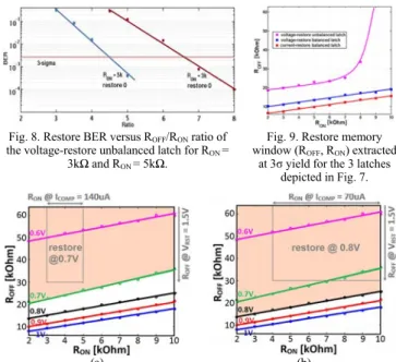
Fig. 8. Restore BER versus ROFF/RON ratio of
the voltage-restore unbalanced latch for RON =
3kΩ and RON = 5kΩ.
Fig. 9. Restore memory window (ROFF, RON) extracted
at 3σ yield for the 3 latches depicted in Fig. 7.
(a) (b)
Fig. 10. Restore memory window evolution vs. supply voltage extracted at 3σ yield for the current-restore symmetrical NVFF: (a) Programming conditions that
ensure successful restore at 0.7V and more; (b) Programming conditions that ensure successful restore at 0.8V and more.
In a restore operation, Q/Qb are initially precharged then released for restoring data. For the voltage-restore unbalanced latch, charging node Q is faster than Qb due to lower PMOS resistance, favoring 1 over 0. Fig.8 shows the 0-restoration BER versus ROFF/RON ratio extracted for two RON values. The results
demonstrate that for a same ratio, higher resistance values lead to better yield by reducing the impact of the parasitic OxRAM access transistor resistance. Fig. 9 shows the extracted (RON,
ROFF) pairs at 3σ yield for the 3 restore design solutions. It shows
that balancing the latch structure enables reducing the required memory window for a same yield. The current restore solution outperforms the voltage-restore architecture.
As depicted in Fig.10, restore operation at 0.7V is successful for RON of 3-5kΩ and ROFF>30kΩ, which is compatible with
OxRAM programming conditions of ISET=140uA and
VRESET=1.5V (Fig.1), enabling 108 endurance cycles. Restore
operation at 0.8V and higher requires RON in 4kΩ-10kΩ range
for 70uA of ISET, resulting in lower programming energy.
B. Reliable store operation
The challenge of programming ReRAM lies in delivering the needed programming voltage and the current to the device, while overcoming the voltage gap between VDD and VDDH. Fig. 11.a. depicts the proposed current programming structure. SET of ReRAM is performed by applying signal set which activates the current source and turns on the transistors in series with ReRAM. At the beginning of the pulse, the device resistance is high and the transistors are sized to provide high VR=VSET. After
the resistance drops, the mirror is working and the current ICS is
copied providing IR = ISET. This structure works as a level-shifter
between VDD and VDDH (set signal levels are 0/VDD), while clamping the programming current (ISET). Both NMOS and
PMOS are used on the programming path, thus avoiding access transistor Vth drop.
(a)
(b)
Fig. 11. Current programming structure: a) Principle (SET); b) Full store circuit for one device (SET path is marked in green; RESET path in blue)
The RESET of ReRAM uses the similar structure, with the inverted top/bottom electrodes. At the beginning of the pulse the mirror is activated providing VRESET, and after the switching the
mirror closes. For complete store operation, device is connected to the pair of current programming structures - one dedicated to SET (green) and another one to the RESET operation, as illustrated in Fig. 11.b. SET and RESET paths are optimized individually in order to balance the different SET/RESET programming conditions.
Due to ReRAM programming voltage requirements, the transistors are stacked and VDDH is chosen to achieve pin-to-pin voltages of all transistors smaller than the recommended maximum voltage for thin gate oxide reliability concerns, while it is high enough to ensure fast and energy efficient store operation.
V. NVFF RESULTS AND DISCUSSION
For the benchmarking, the proposed NVFF is compared to a standard MSFF cell and a dual-rail data-retention latch MSFF [12].
A. Sleep energy
The sleep energy of MSFF depends on the time spent in this mode (tSLEEP) and its retention power supply (VRET):
E V ∙ I t ∙ dt 1
The sleep energy of a data retention latch MSFF cell includes both store/restore transitions (ESTORE, ERESTORE) and the
consumption of the balloon latch in the retention (VRET_BL):
E E E
V _ ∙ I _ t ∙ dt 2
The sleep energy for the proposed dual-rail NVFF is consumed only during the store/restore transition phases. The total sleep energy is:
E E E
E _ E _ E (3)
where ESTORE_VDDH and ESTORE_VDD are the store energy
consumed in the NVFF VDDH and VDD domains, respectively. Fig. 12 shows the time intervals for which the MSFF and the data-retention latch MSFF sleep energies reach the NVFF sleep energy (break-even time) versus the retention supply voltage, when applying 1.5V of VRESET and 85µA of ISET of OxRAM
programing conditions in order to reach 7kΩ (RON) and 200kΩ
(ROFF) of resistance states (Fig.1) ensuring more than 3σ restore
yield. For a system using data retention latch MSFF supplied at 0.5, replacing them with NVFF becomes beneficial for a period of inactivity longer than in average 0.34s for a uniform Q switching (from 0.17s@00 to 0.6s@01). The MSFF exceeds the NVFF consumption after less than 45ms, showing that for normally-off systems characterized by long standby modes NVFF solutions bring considerable energy savings.
B. Active energy
The consumption in active mode is evaluated for 5% data activity and 100% clock activity. Fig.13gives the active energy of NVFF and data retention latch MSFF normalized to standard MSFF cell for 10MHz-1GHz frequency range. The data retention latch MSFF consumption is slightly higher than the MSFF (from 2.55fF 1GHz up to 3.07fF at 10MHz). The NVFF circuit consumes from 3.5% (at 1GHz) up to 20% (at 10MHz) more if VDDH=VDD. The leakage of NVM block is suppressed by completely turning off VDDH. In that case, the power overhead drops to 3.4%@1GHz – 13%@10MHz. The remaining overhead comes from the slave stage modifications and the logic block in the NVFF.
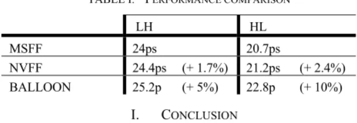
C. Propagation delay
Clk-Q delays (from 40% of clock rising edge to 60% of rising or 40% of falling of the output signal) for low-to-high (LH) and high-to–low (HL) transitions are given in Table I. The delays are estimated for the cells that are driving x4 inverter. Comparing to MSFF, the NVFF does not exhibit significant performance degradation (less than 3%), which makes.
TABLE I. PERFORMANCE COMPARISON
LH HL
MSFF 24ps 20.7ps
NVFF 24.4ps (+ 1.7%) 21.2ps (+ 2.4%)
BALLOON 25.2p (+ 5%) 22.8p (+ 10%)
I. CONCLUSION
The investigation of design architectures and OxRAM programming conditions demonstrates a reliable high-yield low operating voltage thin-gate-oxide transistor NVFF design in 28nm FDSOI technology. The current restore operating mode relies on a quasi-symmetrical latch is demonstrated as the most efficient NVFF design to face OxRAM variability. Reliable on a narrow memory window, it allows both high OxRAM endurance and low data programming consumption. 28nm FD-SOI enables the operation down to 0.7V with more than 108
endurance cycles which corresponds to more than 10 years of operation of s system entering and exiting sleep at break-even time periods. The current-based programming circuit balances SET/RESET programming conditions using low-level voltage control signals. Benchmarked against standard MSFF and the data-retention MSFF, the non-volatility feature comes at the cost of low operating consumption and timing penalty, but provides a significant energy savings for connected devices with long inactivity periods.
Fig. 12. Time intervals for which the MSFF and the data retention latch MSFF sleep energies equal NVFF sleep energy (break-even time) versus the
retention supply voltage (VRET) (Programing pulse width=100ns, Average
swtching time=50ns).
Fig. 13. NVFF and data retention latch MSFF active energy normalized to standard MSFF active energy versus operting frequency.
ACKNOWLEDGMENT
This work has been performed in the ANR project DIPMEM and FP7 project PANACHE with the strong collaboration of STMicroelectronics
REFERENCES
[1] J. Chase, “The evolution of the Internet of Things,” Texas Instruments, September 2013.
[2] I. Kazi, et al., “A ReRAM-based non-volatile flip-flop with sub-Vt read and CMOS voltage-compatible write,” NEWCAS, IEEE, 2013 [3] S. Onkaraiah et al., “Bipolar ReRAM based non-volatile flip-flops for
low-power architectures,” NEWCAS, IEEE, 2012.
[4] E. Vianello et al., “Resistive Memories for Ultra-Low-Power embedded computing design”, IEDM 2014
[5] B.Govoreanu et al., “10x10nm2 Hf/HfOx Crossbar Resistive RAM with Excellent Performance, Reliability and Low-Energy Operation,” Proc. of Electron Devices Meeting, IEDM, 2012.
[6] R. Fackenthal et al., “A 16Gb ReRAM with 200MB/s write and 1GB/s read in 27nm technology,” ISSCC, 2014.
[7] Y. Jung et al., “MTJ based non-volatile flip-flop in deep submicrontechnology,” ISOCC Tech. Dig., 2011.
[8] N. Jovanovic et al., “OxRAM-based non volatile flip-flop in 28nm FDSOI,” NEWCAS, 2014.
[9] N. Planes et al., “28nm FDSOI technology platform for high-speed low-voltage digital applications,” VLSI Technology Dig., pp. 133-134, 2012. [10] Chen et al., “Balancing SET/RESET Pulse for >1010 Endurance in
HfO2/Hf 1T1R Bipolar RRAM, IEEE Transactions On Electron Devices,”
pp. 3243-3249, Vol. 59, No. 12, December 2012.
[11] N. Jovanovic et al., “Design insights for reliable energy efficient non-volatile flip-flop in 28nm FD-SOI,” S3S, 2015.
[12] S. Shigematsu, et al., “A 1-V high-speed MTCMOS circuit scheme for power-down application circuits,”IEEE Journal of Solid-State Circuits, Vol.32, No.6. pp. 861-869, June 1997