HAL Id: tel-00716410
https://tel.archives-ouvertes.fr/tel-00716410
Submitted on 10 Jul 2012
HAL is a multi-disciplinary open access
archive for the deposit and dissemination of sci-entific research documents, whether they are pub-lished or not. The documents may come from teaching and research institutions in France or abroad, or from public or private research centers.
L’archive ouverte pluridisciplinaire HAL, est destinée au dépôt et à la diffusion de documents scientifiques de niveau recherche, publiés ou non, émanant des établissements d’enseignement et de recherche français ou étrangers, des laboratoires publics ou privés.
des rayons X
Francesca Mastropietro
To cite this version:
Francesca Mastropietro. Imagerie de nanofils uniques par diffraction cohérente des rayons X. Physique [physics]. Université de Grenoble, 2011. Français. �NNT : 2011GRENY052�. �tel-00716410�
TH `
ESE
Pour obtenir le grade de
DOCTEUR DE L’UNIVERSIT ´
E DE GRENOBLE
Sp ´ecialit ´e : Physique de Mati `ere Condens ´ee et Rayonnement
Arr ˆet ´e minist ´erial : 7 Ao ˆut 2006
Pr ´esent ´ee par
Francesca Mastropietro
Th `ese dirig ´ee par Jo ¨el Eymery
et codirig ´ee par Vincent Favre-Nicolin et Dina Carbone
pr ´epar ´ee au sein SP2M / UMR-E CEA / UJF-Grenoble 1, INAC, Grenoble,
F-38054, France
et de ´Ecole Doctorale de Physique
Imagerie de Nanofils Uniques par
Diffraction Coh ´erente des Rayons X
Th `ese soutenue publiquement le 4 Octobre 2011, devant le jury compos ´e de :
Sylvain RAVY
Directeur de Recherche CNRS, Universit ´e Paris-Sud, Paris (France), Pr ´esident
Cinzia GIANNINI
Chercheuse CNR, Bari (Italie), Rapporteur
Olivier THOMAS
Professeur IM2NP Marseille (France), Rapporteur
Jo ¨el EYMERY
Chercheur-Ing ´enieur CEA, Grenoble (France), Directeur de th `ese
Vincent FAVRE-NICOLIN
Maitre de Conf ´erence, UJF-Grenoble 1-CEA, Grenoble (France), Co-Directeur de th `ese
Dina CARBONE
Chercheuse ESRF, Grenoble (France), Co-Directeur de th `ese
Till H. METZGER
Contents
Acknowledgements iv
List of Figures vi
List of Tables xv
Introduction 1
1 Imaging the strain at the nanoscale 5
1.1 The origin of the strain . . . 5
1.1.1 Fabrication techniques . . . 6
1.2 Linear elastic theory: Bulk strain tensor . . . 8
1.2.1 Elastic energy . . . 11
1.2.2 Dislocations and defects . . . 12
1.3 Strain in nanowires . . . 13
1.3.1 Strain relaxation and intermixing . . . 14
1.4 Imaging techniques . . . 15
1.4.1 Scanning tunnelling and atomic force microscopy . . 16
1.4.2 Transmission electron microscopy . . . 16
1.4.3 Imaging with X-rays . . . 19
1.5 Coherent x-ray diffraction imaging: from assemblies to single nano-objects . . . 20
1.5.1 The European Synchrotron Radiation Facility . . . . 20
1.5.2 X-ray focusing optics . . . 21
1.5.3 X-ray diffraction on assemblies of nanostructures . . 22
1.5.4 Coherent x-ray imaging of non-crystalline objects . . 25
1.5.5 Coherent diffraction imaging of crystalline structures 26 2 Coherent X-ray Diffraction Imaging 31 2.1 X-ray diffraction . . . 31
2.2 Coherence properties of a Synchrotron radiation . . . 34 i
2.2.1 Temporal and Spatial coherence . . . 35
2.2.2 Mutual coherence function and degree of coherence . 38 2.3 Coherent X-ray Diffraction imaging on strained nano-objects 40 2.3.1 Phase Retrieval Algorithm . . . 42
2.3.2 Experimental requirements . . . 48
2.4 Coherent Diffraction Imaging at ID01: experimental set-up . 50 2.4.1 Optics . . . 51
2.4.2 Diffractometer . . . 52
2.4.3 Focusing optics and nano-positiong stage . . . 53
3 X-rays Propagation and Fresnel Zone Plate 57 3.1 Fresnel and Fraunhofer regime . . . 57
3.2 Theory of Fresnel Zone Plates . . . 60
3.2.1 Diffraction from a grating . . . 61
3.2.2 Fresnel zone plate: working principles . . . 62
3.2.3 Focusing properties of a FZP and Efficiency Issue . . 65
3.2.4 A Fresnel Zone Plate with a Central Stop . . . 67
3.3 The Paraxial Fresnel Free-Space Approximation . . . 69
3.3.1 Propagation of a Plane WaveFront . . . 69
4 Imaging the X-ray beam focused with a Fresnel Zone Plate 73 4.1 Numerical calculations of coherent X-ray propagation . . . . 75
4.1.1 Fully illuminated Fresnel Zone Plate . . . 77
4.1.2 Partially illuminated Fresnel Zone Plate . . . 85
4.2 Imaging the focused complex wavefield . . . 92
4.2.1 Modified Phase Retrieval Algorithm . . . 93
4.2.2 Results and Discussion . . . 95
4.3 Imaging the coherent beam using Bragg Ptychography . . . 98
4.4 Conclusions . . . 102
5 Coherent diffraction imaging on strained nanowires: be-yond the ideal case 103 5.1 Time-dependent analysis on the strain evolution of sSOI lines 103 5.1.1 Engineered strain in sSOI: sample description . . . . 104
5.1.2 Experiments . . . 107
5.1.3 Finite element method: calculations . . . 108
5.1.4 Data analysis . . . 113
Contents iii
5.3 Nanowires with stacking faults . . . 124
5.3.1 CDI on InSb/InP nanowires with stacking faults . . . 129
6 Imaging the strain in single GaAs nanowires with InAs Quantum Dots and Quantum Well 137 6.1 Introduction . . . 137
6.2 Numerical calculations . . . 138
6.3 Experiment . . . 140
6.3.1 Collecting 3D scatterings in Bragg geometry . . . 141
6.3.2 Sample description . . . 143
6.3.3 Experimental data . . . 145
6.3.4 Data treatment . . . 148
6.4 Two-dimensional Ptychography in Bragg geometry . . . 150
6.5 Conclusions . . . 154
Conclusions and overview 159
A The Huygens-Fresnel principle 161
B New diffractometer at the undulator beamline ID01 165
C Orthonormalisation process for energy scan 169
Bibliography 171
Acknowledgements
Several people have contributed to the realization of my thesis. I am grateful to Dr. Vincent Favre-Nicolin, Dr. Jo¨el Eymery and Dr. Till Metz-ger who offered me the possibility of joining their research groups and wor-king in a great collaboration. I was impressed by their passion for science and their human qualities. I really appreciated their pedagogy and their patience. Thanks for everything you taught me.
I warmly acknowledge Dr. Dina Carbone, that was for me not only a continuous source of scientific knowledge and motivation but also a very kind friend. Thanks for sharing the chaos of the office with me during the last two years and for your good mood.
I also had the chance to work with Dr. Virginie Chamard. I really thank her for the interest she showed in my research and the fruitful discussions in Marseille. I want to thank also Dr. Ana Diaz for her scientific support at the beginning of my PhD and for the unforgettable nights we spent in Grenoble.
I would like to thank Dr. Cinzia Giannini, Prof. Olivier Thomas and Dr. Sylvain Ravy for the careful reading of the manuscript and for their presence in the examination jury.
I express my gratitude to the people I met at the INAC laboratory of the CEA and the staff of ID01 for their support during experiments.
My warm thanks go to all my friends and to Piero, without them life in Grenoble would not be so amazing!
I cannot forget all the people I left in Italy. A lovely thought goes my parents, Pino and Annalisa, my sister Teresa and my brother in law Nick, who always believed in me and for the unconditional love they give me every day, to my niece Nicole and to Ester and Felice...I missed all of you a lot during my stay in France.
1.1 The use of bottom-up and top-down techniques in manufacturing.
(http://www.nanotec.org.uk/finalReport.htm) . . . 6
1.2 Schematics of bottom-up process to growth Si nanowires
from metallic catalysts with a hetero-insertion (modified from
http://fillergroup.gatech.edu/research). . . 7
1.3 Schematics illustrating top-up (lithography) process to fabricate nano
electro-mechanical systems (NEMS) (S. Afr. J. Sci. 104, 5-6, 2008). . . . 7
1.4 Action of the bulk stress σij on an elementary cube. The index i refers
to the direction Xi where the stress acts while j gives the direction
perpendicular to the three front faces. . . 8
1.5 Sketch of the coherent accommodation in the hetero-epitaxial deposition
of a layer with an unstrained lattice parameter aunstron a substrate with
lattice parameter abulk. The lattice aunstr shrinks due to the effect of
the strain.(Modified from [Malachias, 2005]) . . . 11
1.6 Pure edge (left) and pure screw (right) dislocations. [Tsao, 1992] . . . . 12
1.7 Heterogeneous nanowires. (a) Growth through catalyst-mediated axial
synthesis. (b,c) Axial and radial heterojunction. (d,e) Axial superlattice
and radial heterostructure (core-shell). [Hayden et al., 2008] . . . 13
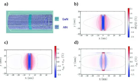
1.8 a) AlN nanowire with a 5 nm thick GaN insertion. b) Hydrostatic
defor-mation, c) in-plain strain ǫxx+ ǫyyand d) vertical strain ǫzzin AlN/GaN
nanowires. (Modified from [Camacho, 2010]) . . . 15
1.9 Left: Coherent electron diffraction pattern recorded from a single,
faceted, Au nanocrystal (≈3.5 nm in diameter) at the (111) reflec-tion. Right: The experimental (left) and simulated (lower right) high-resolution TEM images and the Au nanocrystal model (upper right).
The scale bar is 2 nm. [Huang et al., 2008] . . . 17
1.10 Surface atom displacements shown as vectors for atoms possessing a coor-dination number less than 9 (left, mostly are 100 atoms and neighbouring vicinal facet atoms) and equal to 9 (right, mostly are 111 surface atoms). Here, the magnitudes of the displacements are rendered using colours. Also directions of the surface atom displacements is represented by
ar-rows. [Huang et al., 2008] . . . 18
1.11 Tunable undulator radiation generated by the passage of relativistic
elec-trons through a periodic magnet structure [Attwood et al., 1993] . . . . 21
1.12 Average brilliance of third generation synchrotron radiation sources.
(http://hasylab.desy.de) . . . 22
List of Figures vii
1.13 X-ray focusing optics: schematics of : a)
Kirkpatrick-Baez mirrors, b) compound refractive lenses and c)
Fres-nel zone
plate.(http://www.xradia.com/technology/basic-technology/focusing.php) . . . 23
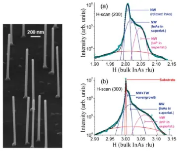
1.14 Left: Scanning electron microscopy images of CBE grown epitaxial InAs/InP nanowires. Right: In-plane measurements along h for the (a)
(200) and (b) (300) reflections. [Eymery et al., 2007] . . . 24
1.15 Left: A diffraction pattern of the specimen (using a logarithmic intensity scale). Right: The specimen image as reconstructed from the diffraction
pattern. [Miao et al., 1999] . . . 25
1.16 Left: Soft x-ray diffraction pattern of a freeze-dried yeast cell. Right:
Images of the reconstructed freeze-dried yeast cell. [Shapiro et al., 2005]) 25
1.17 Maximum value projections along three orthogonal directions of the re-constructed 3D non-periodic object. Projections were performed along (a) z, (b) x, and (c) y directions. The scale bars are 500 nm. [Chapman
et al., 2006b] . . . 26
1.18 Phase map of a slice through a 200 nm Au nanocrystal obtained by hybrid inputoutput inversion of its coherent pattern measured with the (111) Bragg peak using a focused x-ray beam. [Robinson and Harder, 2009] 27 1.19 Two-dimensional slices of the six independent components of the strain
tensor.[Newton et al., 2010] . . . 28
1.20 (a) Reconstructed vertical component µz of the dispacement field in a
(Ga,Mn)As/GaAs nanowire. (b) Numerical calculation of µzusing finite
element methods. [Minkevich et al., 2011] . . . 28
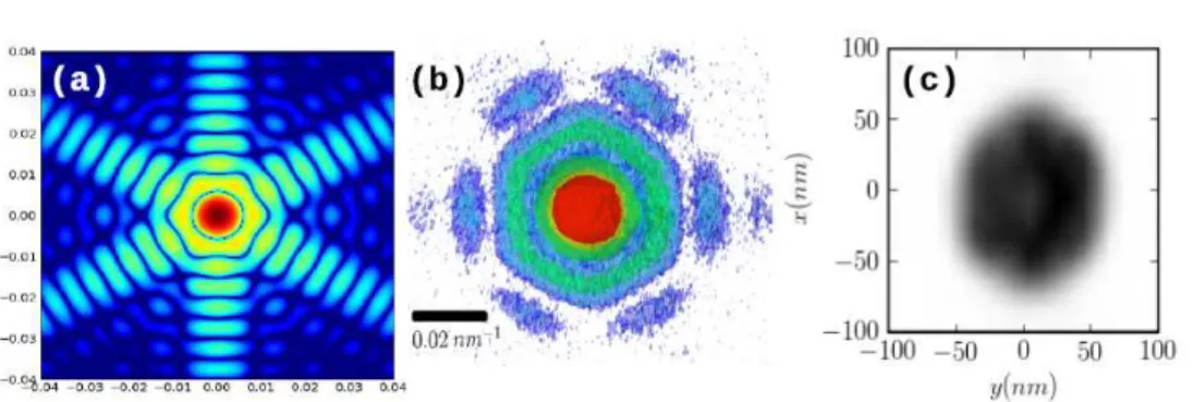
1.21 CDI of a single Si nanowire: (a) simulated 2D scattering pattern (in the plane perpendicular to the nanowire axis), (b) experimental pattern recorded on a 95 nm silicon nanowire and (c) the corresponding
real-space reconstruction of the nanowire cross-section . . . 29
1.22 (a) Retrieved complex-valued electron density and (b) phase of the wire section. Scales in both a and b are linear. The dashed square indicates
the support region used in the reconstruction algorithm. [Diaz et al.,
2009] . . . 30
2.1 Bragg scattering geometry : the incident beam is scattered by atoms of
parallel atomic planes. The length path difference between two scattered beams can be used to determine the atomic distance d of two atomic planes. 32
2.2 Two-dimensional Ewald sphere: Bragg condition is satisfied for any
point of the circle, overlying point on the lattice in the reciprocal space
S(hk)=G(hk). . . 33
2.3 Young’s Double slits experiment: the interference pattern from two slits
separated by a distance d. Slits are illuminated by the central part (solid
line) and the edge (dotted line) of the source a. . . 35
2.5 Two quasi-monochromatic waves of wavelenght λ and λ + ∆λ. The difference in phase is π at the longitudinal coherence length. [Dierolf,
2007] . . . 37
2.6 Representation of Error-Reduction phase retrieval algorithm. Starting
with an arbitrary guess, it consists of several loop between real and reciprocal space by means of Fourier Transformation back and forth and
applying in each spaces a set of constrained. . . 44
2.7 Overview of the Optics and Experimental hutches (http://www.esrf.fr) . 51
2.8 Measured visibility of the moir´e fringes pattern for the CCM (in blue)
and the DCM (in red). The envelope functions were fitted to Gaussian curves (dashed lines) and give a measurement of the complex coherence
function in the vertical direction. [Diaz et al., 2010] . . . 52
2.9 (a) The 4+2-circles diffractometer and (b) the Huber Tower
[O. Plantevin, 2008]. . . 53
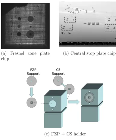
2.10 Silicon membrane chips with a series of (a) gold Fresnel Zone Plates and (b) gold central stops. The outer most zone is 100 nm for all lenses and diameters varies from 20 to 200 µm. (c) FZP and CS holder designed
for ID01. . . 54
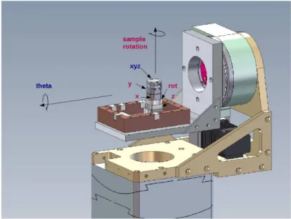
2.11 Schematic of holder and sample stage implemented in the Huber Tower. 55
3.1 Three different methods to probe the separation between Fresnel and
Fraunhofer diffraction, changing: a) the position of the detector, b) the
wavelength and c) the opening of the slit. ( [Jacques, 2009]) . . . 58
3.2 Vertical profiles of the calculated (blue line) and the measured (black
line) wavefronts using the experimental method in Fig. 3.1c. ( [Jacques,
2009]) . . . 59
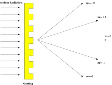
3.3 Sketch of a binary diffraction grating. . . 61
3.4 Monochromatic plane wave diffracted in a series of diffraction order from
a grating. . . 62
3.5 Two examples of Fresnel Zone Plate: circular (left) and parallel (right)
geometry. [David et al., 2001] . . . 63
3.6 Fresnel Zone Plate lenses are used to image an x-ray source S in the
image point P; a’ and b’ are the characteristic distance to the object and
the image, respectively. [Attwood, 1999] . . . 63
3.7 Fresnel Zone Plate diffracting focusing for 1st, 3rd, 5th orders.(Modified
from http://ast.coe.berkeley.edusxreuv/2005/) . . . 65
3.8 Radial intensity distributions for obstruction ratios aCS = 0, 0.6 and
0.9. The main plot shows each distribution normalized to its own central peak, while the inset shows the central peaks each normalized to that for
aCS=0. (Modified from [Simpson and Michette, 1984]) . . . 68
3.9 Schematic of the zone plate and order sorting aperture setup. (Modified
from [Kirz et al., 1995]) . . . 68
3.10 Diffraction geometry : P1 is a generic point of coordinates (ξ, η) and P0
List of Figures ix
4.1 (a) Sketch of a partially illuminated Fresnel Zone Plate. A pair of slits
defines a rectangular aperture matching the transverse coherence lengths of the x-ray beam. (b) 2D schematic of the propagation of the wavefield produced by a partially illuminated FZP. The slits, placed 1.15 m up-stream the lens, used to define the illuminated area, the FZP, the CS and the OSA are represented. The effective direction of propagation is tilted with respect to the FZP axis due to the lateral displacement of the
slits. . . 75
4.2 Diffraction efficiencies (first order) of various FZPs with an outermost
zone width dr, diameter D and zone height H measured over a wide range of X-ray energies and compared with the theoretical maximum values calculated from the tabulated X-ray optical constants. [Gorelick
et al., 2011] . . . 76
4.3 Radii dependence on the number of zones. . . 78
4.4 One-dimensional sketch of the calculation of a wavefield propagating
from the Fresnel zone plate to detector position. . . 79
4.5 (a) Phase and (b) amplitude in logarithmic scale of the complex field
plotted in the plane xz. A central stop and a order sorting aperture with a diameter of 65 µm and 50 µm, respectively, are included in the
simulations. . . 81
4.6 (a) Simulated phase and (b) amplitude (logarithmic scale) at the focus
of a Fresnel Zone Plate. A central stop and an order sorting aperture with a diameter are included in the simulations. Horizontal cuts of (c)
calculated phase and (d) amplitude (logarithmic scale) . . . 82
4.7 Profiles of (a) calculated phase and (b) amplitude (logarithmic scale)
using a 1D dimensional FZP. . . 82
4.8 (a) Simulated two-dimensional phase (logarithmic scale) and (b)
inten-sity of the calculated complex field at the detector position. The cylin-drical symmetry and the constant phase are preserved along the propa-gation. Horizontal cuts of (c) calculated phase and (d) intensity
(loga-rithmic scale) at the detector plane. . . 84
4.9 Simulated complex field in the vicinity of the focus of a Fresnel Zone
Plate. The focal length are strongly influenced by the presence of the slits. Calculations have been computed for three different slits opening: (a,d) 120v× 60h, (b,e) 60v× 20hand (c,f) 40v× 20hµm2. Cuts in (a-c)
the horizontal (xz) and (d-f) vertical (yz) planes. . . 86
4.10 Simulated complex field at the focal plane: (a,b,c) amplitude (in loga-rithm scale) and (d,e,f) phase the focal spot size for three different slits opening: (a,d) 120v× 60h, (b,e) 60v× 20hand (c,f) 40v× 20h µm2. For
each opening, the central peak shows a constant phase and focal spot
size are found inversely proportional to the slit openings. . . 87
4.11 Simulated phase at the focal plane without correction for the slit opening
4.12 Simulated complex field at the focus of a Fresnel Zone Plate: (a,b,c) cuts in the vertical (y) and (d,e,f) in the horizontal directions. Calculations
have been computed for three different slits opening: (a,d) 120v× 60h,
(b,e) 60v× 20hand (c,f) 40v× 20hµm2. . . 88
4.13 Amplitude (expressed in logarithmic scale) of simulated complex field at the FZP plane considering the propagation from the slits distant 1.15 m: cut in the (a) horizontal and (b) vertical directions. An opening of
72v× 28hµm2 corresponding to the experimental opening. . . 89
4.14 Simulated complex field at the focal plane when slits are distant 1.15 m from the FZP plane: calculated amplitudes (in logarithm scale) in the (a) xz, (b) yz and (c) xy planes are shown. (d) Calculated phase in the xy plane is found to be constant. (e,f) Vertical and horizontal cuts of
the focal spot show a spot size of 300v× 800hnm2. . . 90
4.15 Simulated 2D intensities at the detector plane when (a) slits are at the
FZP plane and (b) 1.15 m before the lens. . . 91
4.16 Phases of simulated wavefield at the detector plane for (a) partially il-luminated FZP (b) including the propagation of the wavefield from the
slits to the lens plane. . . 91
4.17 (a) Experimental intensity in the divergent part of the focused beam compared to (b) calculations. (c) Horizontal and (d) vertical cuts for experimental intensity and simulated one when slits are 1.15 m distant
from the FZP. . . 92
4.18 Scheme of the two-steps phase retrieval algorithm used to reconstruct
the complex wavefield at the focal plane. . . 94
4.19 (a) Phase and (b) amplitude of the reconstructed complex wavefield at
the focus and (c) along the direction of propagation. . . 95
4.20 (a) Horizontal and (b) vertical cuts of the reconstructed complex wave-field at the focus compared to the one computed considering a slit open-ing of 72v× 28hµm2. . . 96
4.21 (a) Amplitude (b) and phase of the reconstructed complex wavefield at
the zone plate plane. . . 97
4.22 Part of the metric error R registered during the reconstruction.
Contri-butions from ER, HIO and CF algorithms are labelled. . . 97
4.23 (a) Experimental data used to reconstruct (b) amplitude (logarithmic scale) and (c) phase of the complex wavefield at the focus in the case of
a fully illuminated Fresnel zone plate with a fully coherent beam. . . 98
4.24 Schematic of the ptychographic approach. The beam moves from posi-tion 1 to N to cover the surface of the chosen zone on a sample, in that
case a schematically depicted double Si lines. . . 99
4.25 Top: Electron microscopy of the <110>-oriented Si double-line. Bottom: Atomic force microscopy of the exploited region. . . 100 4.26 Color rendition of the reconstructed probe at the sample position. The
retrieved illumination function is shown in the plane perpendicular to the X-ray beam propagation. . . 101
List of Figures xi
5.1 Schematic (front view) of the patterned sSOI lines. (Modified from
[Bau-dot et al., 2009]) . . . 105
5.2 Schematic of the fabrication process of strained Si ultrathin layers
di-rectly on oxide by using thin layer transfer. (a) Growth of the relaxed
Si1xGex virtual substrate; (b) growth of the biaxially tensile strained
Si on the Si1xGex virtual substrate;(c) hydrogen ion implantation into
the grown heterostructure; (d) bonding of the hydrogen implanted het-erostructure to a SiO2/Si substrate; (e) thermal annealing induced layer exfoliation around the hydrogen implantation depth; (f) thin strained
Si layer directly on SiO2/Si obtained after the removal of the residual
Si1xGex.( [Moutanabbir et al., 2010]) . . . 106
5.3 Strain calculated from GIXRD in-plane measurements as a function of
the sSOI line width with a height of 70 nm along and perpendicular to the lines. R2 is the planar reference before the lines etching. (Modified from [Baudot et al., 2009]) . . . 107
5.4 Sketch of the experimental set-up. The coherent beam is focused with
a FZP. Lines are placed at the focal position parallel to the beam. The
typical scattering registered for the (1¯13) Bragg reflection is also shown. 108
5.5 Simulated displacement field, using FEM in the trapezoidal section of
the line in the (x, z) plane. The calculated displacements is relative to a
bulk Si1−xGex lattice. (Courtesy of S. Baudot) . . . 109
5.6 Left: Color rendition of the complex-valued 2D diffraction pattern
calcu-lated from the displacement field depicted in Fig. 5.5 for the (1¯13) Bragg
reflection. Right: Color rendition of the complex object in the direct space, calculated through the back Fourier transform from scattering to the left. . . 109
5.7 a) The measured scattering for a single line is compared to b) the
calcu-lated 2D reciprocal space map for the (1¯13) Bragg reflection. . . 110
5.8 a) Mapping in real space for the (1¯13) Bragg reflection around different
lines. Colours correspond to the total intensity received by the detector at a given sample position. Intensity is expressed in logarithmic scale. b) SEM image of the Si-lines. The irregularity of the lines is due to the mechanical drift of the piezostage during measurements. . . 111
5.9 Calculated complex-valued function at the sample position from FT of
complex scattering (Si line). Calculated complex-valued function at the detector (Acalc) from a FT of the fit using the asymmetric polynomial
representation of the displacement uz. Phase is represented by colours
and intensity (expressed in logarithmic scale) by the intensity of the colours. Two dimensional diffraction patterns collected for the chosen silicon line at the time T=0 sec (Iobs) compared to the calculated in-tensity (Icalc). Intensities are expressed using the same logarithmic scale. 112
5.10 Calculated complex-valued function at the sample position from FT of complex scattering (Si line). Calculated complex-valued function at the detector (Acalc) from a FT of the fit using the asymmetric polynomial
representation of the displacement uz. Phase is represented by colours
and intensity (expressed in logarithmic scale) by the intensity of the colours. Two dimensional diffraction patterns collected for the chosen silicon line at the time T=800 sec (Iobs) compared to the calculated intensity (Icalc). Intensities are expressed using the same logarithmic
scale. . . 113
5.11 Calculated complex-valued function at the sample position from FT of complex scattering (Si line). Calculated complex-valued function at the detector (Acalc) from a FT of the fit using the asymmetric polynomial
representation of the displacement uz. Phase is represented by colours
and intensity (expressed in logarithmic scale) by the intensity of the colours. Two dimensional diffraction patterns collected for the chosen silicon line at the time T=1600 sec (Iobs) compared to the calculated intensity (Icalc). Intensities are expressed using the same logarithmic
scale. . . 114
5.12 Calculated complex-valued function at the sample position from FT of complex scattering (Si line). Calculated complex-valued function at the detector (Acalc) from a FT of the fit using the asymmetric polynomial
representation of the displacement uz. Phase is represented by colours
and intensity (expressed in logarithmic scale) by the intensity of the colours. Two dimensional diffraction patterns collected for the chosen silicon line at the time T=2900 sec (Iobs) compared to the calculated intensity (Icalc). Intensities are expressed using the same logarithmic
scale. . . 115
5.13 Displacement field uz obtained from the time-dependent analysis of
ra-diation damage at different time: a) T= 0 sec, b) T= 800 sec, c) T= 1600 sec and d) T= 2900 sec. Colours represent scale units expressed in
nanometres. . . 117
5.14 Strain fields ǫzz and ǫzx from time-dependent analysis of radiation
dam-age at different time: a) T= 0 sec, b) T= 800 sec, c) T= 1600 sec and d) T= 2900 sec . . . 118 5.15 Calculated two dimensional diffraction patterns obtained through a FFT
of the wire section multiplied by the illumination function with a constant phase within the focal spot. . . 120 5.16 Calculated two dimensional diffraction patterns obtained through a FFT
of the wire section multiplied by the illumination function with a
Gaus-sian phase within the focal spot. . . 120
5.17 Calculated two dimensional a) amplitude and phase in real space. Phases in b) and c) are obtained by Fourier transforming the complex scattering in Figs. 5.15 and 5.16, respectively. . . 121
List of Figures xiii
5.18 Calculated displacement field from the phases shown in Fig. 5.17
ob-tained for the investigated Bragg reflection (1¯13). The displacement
field 3uz contains the contribution of the illumination function. . . 122
5.19 Schematics of the contributions (amplitude and phase) of the coherent probe along the sSOI lines. In this direction, the phase variation of the probe has to be taken into account to study the influences of the illumination when a CDI approach is used to investigate the nanostructure.123 5.20 Atomistic simulations of an InAs wurtzite nanowire (diameter = 60 nm,
height = 100 nm) with (a)-(d) a 3 nm and (e)-(h) a 15 nm InP insertion: (a, e) the radial displacement (along [110], expressed relatively to the perfect InAs lattice, in unit cells), (b, f) the axial displacement (along [001]), the calculated intensities around the (c, g) (004) and (d, h) (202) reflections, with a logarithmic colour scale. The map coordinates are
given in reciprocal lattice units (r.l.u.) relative to InAs. . . 125
5.21 Simulation of the influence of stacking faults on the coherent scattering from InAs/InP nanowires (diameter = 60 nm, height = 100 nm) around
a (202)W Z reflection. 2ux + 2uz for (a) the original InAs/InP nanowire
obtained using atomistic simulations, and in the case of (d) one and (e) three stacking faults. The colour scale is expressed in unit cells (u.c.) and is the same for (a, d, e). The resulting scattered intensity is shown in (b) (one fault) and (c) (three faults). Complex recovered density (see text for details) is shown in the case of one (f) and three (g) faults. In these images the phase is given by the colour (as indicated by the colour wheel), while the amplitude is given by the saturation of the colour. . . 127 5.22 Left: HRTEM image in the [110] direction of the InSb-InP interface. The
stacking faults is present in the InSb part close to the interface. Right: X-ray energy dispersive measurements of the heterostructure. (Modified from [Borg et al., 2009]) . . . 130 5.23 Top: Reciprocal space map (h0l) collected on an assembly of InSb/InP
nanowires during a GIDX experiment on BM32 (ESRF). Bottom: (10l) truncation rods for InP and InSb. Measurements have been done on the
same beamlines at three different incident angles αc: 0.00◦, 0.05◦ and
0.10◦. . . 131
5.24 CXDI set up used to probe a single InSb/InP nanowire. . . 132 5.25 2D coherent diffraction images of a single InSb/InP nanowire . Scattering
from (111) reflection has been collected for the InSb (right) and the InP (left) sections of the same nanowire. The illuminated InSb section is certainly faulted as the strong asymmetry in the intensity distribution shows. . . 133
5.26 Experimental diffraction image from an InSb/InP nanowire at (3¯33)ZB
Bragg reflection, measured at the top (left) and bottom (right) (near the InSb/InP interface) of the InSb section. . . 133 5.27 Left: Simulated deformation as a function of the height near the base
of the InSb section (height = 250 nm). Right: Calculated scattering corresponding to the deformation depicted to the left. . . 134
6.1 The projected side view along the [001] direction of 1 ML InAs buried between the GaAs cap layer and buffer layer. The substrate GaAs diffrac-tion planes are indicated by bold lines while the dashed lines indicate the indium position and the position for the arsenic in the cap. The displace-ments of the In atoms and the cap As atoms are also represented with respect to the (004) diffraction planes [Lee et al., 1996]. . . 139
6.2 a) Color rendition of the calculated 2-dimensional GaAs nanowire with
a monolayer of InAs QDs for the (004)InAs Bragg reflection. Phase is
represented by colours. b) 2-dimensional intensity in reciprocal space calculated with a FT of the complex object in real space shown in a). . . 139
6.3 Simplified schematics in reciprocal space for (a) a rocking-curve scan, (b)
an energy scan and (c) a θ−2θ scan. The dashed and dotted lines indicate the variation of the incident and diffracted beams. The movement of the detector (as projected on the Ewald’s sphere) is also illustrated. . . 142
6.4 Scanning electron microscopy of the investigated array. . . 144
6.5 Scanning electron microscopy images of the investigated nanowire with
InAs QDs. Left: Top view. Right: Side view (with an angle of 51◦) of
the same wire. . . 144
6.6 Scanning electron microscopy images of the investigated nanowire with
InAs QW. . . 145
6.7 Vertical scan along the nanowire from a) the bottom to f) the top. Each
raw image has been collected using 200 nm motor step and acquisition time of 20 s. The QDs are inserted at a position between the scatterings depicted in c) and d). A selection of 150×150 pixels on the detector is shown. . . 147
6.8 3-dimensional diffraction pattern (not orthonormalised) collected at the
QDs position for the (004)GaAs Bragg reflection using the energy scan in
a range of ± 50 eV with a step of 1 eV and acquisition time of 5 s. The splitting of the central peak close to 10 keV is evident in figures b) and c). . . 148
6.9 3-dimensional diffraction pattern (not orthonormalised) collected at the
QDs position for the (004)GaAs Bragg reflection using the rocking scan
in the angular range of 0.60◦ with a step of 0.005◦ and acquisition time
of 20 s/step. . . 149 6.10 2D scatterings (raw data) from a vertical scan along the GaAs wire with
InAs QDs insertion plane shown in Fig. 6.5 and used for ptychography. On the horizontal and vertical axis the number of selected pixels at the detector plane. . . 151 6.11 2D scatterings (raw data) from the vertical scan along the GaAs wire
with InAs QW insertion shown in Fig. 6.6 and used for ptychography. On the horizontal and vertical axis the number of selected pixels at the detector plane. . . 152
6.12 Preliminary results from ptychography analysis of the diffraction pat-terns shown in Fig. 6.10. The phase shift occurs at z ≈ −100 nm. Phase is expressed in radians. The reconstructed shape is in agreement with the one shown in Fig. 6.5b. . . 153 6.13 Preliminary results from ptychography analysis of the diffraction
pat-terns shown in Fig. 6.11. The phase shift occurs at z ≈ −100 nm. Phase is expressed in radians. The reconstructed shape is in agreement with the one shown in Fig. 6.6. . . 154
A.1 Illustration of the Fresnel-Kirchhoff diffraction integral (geometry of a
single slit) using boundary values problem proposed by Kirchhoff. . . 162
A.2 Schematics of the Huygens-Fresnel principle using the boundary
condi-tions in [Marchand and Wolf, 1966]. . . 162
B.1 Schematic view of the new diffractometer. . . 167
B.2 Zoom view on the sample stage. . . 167
C.1 Description of a monochromatic wavefield impinging on a sample, that
is placed at the centre of the Ewald sphere, with all orientational pa-rameters needed to describe the experiment: δ, ν define positions on
the detector placed at the sample-detector distance D, and X0, Y0, the
coordinate system on the detector. The pixel size is indicated by pxlsize 170
List of Tables
4.1 Features used for numerical calculations. . . 77
4.2 Values of beam size and focal depth calculated for different illumination
conditions. Calculated phases at the focal spot is also tabulated. The
ideal case of a fully illuminated FZP is shown for comparison. . . 85
5.1 Mean valued calculated for ǫzx and ǫzx at t=0, 800, 1600 and 2900 sec. . 118
B.1 Specifications for the new diffractometer. . . 168
B.2 Specifications for the detector arm. . . 168
Introduction
During the last decade, the interest in semiconductor nanostructures increased enormously, mainly due to their different applications in optical and electronic micro devices. The continuous demand of high performing functional materials gave rise to the development of engineering techniques aimed to the controlled fabrication of nano-objects getting rid of strain and defects. On the other hand, experimental evidences of the improvement of interesting physical properties was showed in the case of strained crystal with respect to the unstrained case.
In this context, the development of characterisation methods with the adequate resolution at the nanometre scale and high strain sensitivity was necessary. Among them, imaging techniques were developed to obtain surface morphology characterisation, as in the case of scanning transmis-sion and atomic force microscopy, and internal structure investigation. In the particular case of strain determination, scattering based techniques, as transmission electron microscopy (TEM) and x-ray diffraction, are largely applied. The first has the advantage of being an imaging technique with atomic resolution and good strain sensitivity. The second provides an ex-tremely high strain sensitivity but is based on indirect model-dependent methods. Nevertheless, x-ray diffraction represents the method of choice to circumvent some limitations of TEM in term of penetration depth and radiation damage.
The wide use of x-ray-based methods to study nanostructures has been also possible due to the development of synchrotron sources combined with the employment of dedicated focusing optics such as Fresnel zone plate to obtain high brilliant radiation with high coherent properties in a micro-sized focal spot. In particular, the use of coherent x-ray beams is at the basis of lens-less microscopy techniques as coherent diffraction imaging (CDI) that allows the model free investigation of a crystal at the nanoscale. Phase retrieval algorithms are used to retrieve at the sample position the complex
exit wavefield from the measurement of far-field coherent intensity patterns, collected in the forward direction (to get morphological information) or in Bragg geometry (that gives access also to the strain fields). In the latter, the strain fields are encoded in the phase of the reconstructed complex-valued function at the sample position. However, this phase also brings the information of the illumination function that needs, therefore, to be taken into account for the correct interpretation of the strain.
The work presented in this manuscript aims to the demonstration of the experimental feasibility of the CDI approach in Bragg condition to re-cover the strain in single heterogeneous or highly strained homogeneous nanowires. In addition, the characterisation of the illumination function in the particular experimental conditions is offered in order to disentangle the different contributions in the retrieved phase.
In Chapter 1, I discuss the scientific motivation of this work. I first recall some theoretical concepts to describe the stress in a crystal and then, using examples from literature, I describe how the strain can be investigated in single nanowires using coherent diffraction techniques.
In Chapter 2, the basic principles of x-ray diffraction and the coherence properties of x-rays produced in a synchrotron facility are reviewed in order to introduce the coherent x-ray diffraction imaging technique. The experi-mental set-up used for coherent experiments at the undulator beamline ID01 at the European Synchrotron Radiation Facility is also described.
In Chapter 3 the working principles of a Fresnel zone plate, a “perfect” diffractive optic used to focus the beam during the described experiments, are detailed. Moreover, the paraxial Fresnel free-space approximation is discussed as an essential theoretical tool to explain the propagation of x-rays with a small deviation from a central axis.
Chapter 4 is dedicated to the study of focused X-ray beam obtained from the partial illumination of a Fresnel Zone Plate: as x-rays produced in a synchrotron facility only present finite coherence lengths, the coherent part of the beam is selected by means of an opening matching the trans-verse coherence length of the available radiation. This partial illumination condition affects the wavefront of the focused x-ray beam with a consequent modification of the exit wavefield. Using both numerical (calculations) and experimental (ab initio reconstruction) approaches, I have determined the illumination function (phase and amplitude) at the focal point.
List of Tables 3
systems presenting specific experimental issues. First, I present a study of the radiation damage observed in strained silicon line, with a time-dependent experiment allowing to recover the strain field as a function of the radiation damage. Then, I demonstrate, through numerical calculations, how the illumination function influences the recovered strain field. Finally, I show that it is possible to image the strain in InSb/InP nanowires even in the presence of stacking faults, by choosing a Bragg reflection insensitive to such defects.
Chapter 6 shows the preliminary results obtained from the measurement of the displacement field in single 300 nm diameter GaAs nanowires with a single layer of InAs quantum dots or quantum well. I show that the recorded coherent diffraction data can be used to determine the thickness and the phase shift in the nanowire and localise the insertion smaller than the achievable resolution.
Chapter 1
Imaging the strain at the
nanoscale
As stated in the Introduction, the aim of this work is to study the dis-placement field in strained nanostructures using coherent diffraction imag-ing technique. In this chapter, I will give a short overview to understand the structural and physical properties of materials described in this work as object of strain determination. I will first recall some theoretical concepts to describe the stress and the strain in a crystal. Then, I will describe typ-ical imaging techniques used to characterize nanostructures. Finally, I will show some interesting example from literature concerning the investigation of the strain in single nanowires using coherent diffraction technique.
1.1
The origin of the strain
The increasing interest in semiconductor nanowires [Samuelson, 2003], nanocrystals [Wang et al., 2005] and nanotubes [Ouyang et al., 2002], dur-ing the last decade [Smith, 1979] can be first attributed to their attractive potential applications [Thelander et al., 2006]. New structures are provided to create artificial potential for charge carriers (both electrons and holes) in semiconductors at a scale comparable to the de Broglie wavelength; quan-tum confinement effects [Kaufmann et al., 2001] become important and the electronic and optical properties deviate substantially from those of bulk material. In addition, new combination of defect-free materials allows get-ting original band gap alignment. Moreover, semiconductors are nowdays an integral part in our practical lives. The challenging down-scaling of electronics and optical devices paved the way to the tremendous
Figure 1.1: The use of bottom-up and top-down techniques in manufactur-ing. (http://www.nanotec.org.uk/finalReport.htm)
ment of nanostructure engineering for electronic and optoelectronic nano-semiconductors [Mokkapati and Jagadish, 2009, Thelander et al., 2006, Li et al., 2006] that could enable new applications in the future. The demand for ever more powerful systems has enhanced the controlled fabrication of nanoscale systems to obtain desired performances, as in the case of het-erostructure nanowires [Caroff et al., 2009, Tomioka et al., 2008]. Concern-ing the growth of functional materials the main problem of crystal growers was for many years to get rid of defects and stress. However, it has been shown in some systems that the stress may not be detrimental to the phys-ical properties (optphys-ical and electronic) of strained crystals when they are carefully controlled. Consequently the device performances may sometimes be improved with respect to the case of unstrained crystal, as shown for the mobility in transistor heterostructures [Jain and Hayes, 1991, Sander et al., 1998, Baudot et al., 2009].
1.1.1
Fabrication techniques
The techniques developed to create nanostructures can be divided in two categories : “bottom-up” and “top-down”. A diagram illustrating the princi-ple of these two approaches is shown in Fig. 1.1. Bottom-up manufacturing involves the building of structures, atom-by-atom or molecule-by-molecule, for example chemical synthesis, self-assembly or positional assembly. The latter consists of the self-assembly directional growth achieved by the pres-ence on the substrate of catalysts (metal droplets), or patterning (holes in the substrate). An example of nanostructure grown through bottom-up method is shown in Fig. 1.2. The depicted case is the vapor-liquid-solid (VLS) deposition to grow Si nanowires from metallic catalysts with a
1.1. The origin of the strain 7
Figure 1.2: Schematics of bottom-up process to growth Si nanowires from metallic catalysts with a hetero-insertion (modified from http://fillergroup.gatech.edu/research).
hetero-insertion. Bottom-up techniques are especially suitable to grow het-erostructures with one or multi heterojunctions, to obtain complex systems. Top-down manufacturing, also known as step-wise design, creates nanos-tructures from a larger material through etching, milling or machining. This approach has been highly refined by the semiconductor industry over the past 30 years, in terms of high precision techniques, such as lithography. Top-down methods offer reliability and device complexity, although they are generally higher in energy usage, and produce more waste than bottom-up methods. An example of nanostructure grown through top-down method is shown in Fig. 1.3. In that case lithography is used to fabricate nano
Figure 1.3: Schematics illustrating top-up (lithography) process to fabricate nano electro-mechanical systems (NEMS) (S. Afr. J. Sci. 104, 5-6, 2008).
Figure 1.4: Action of the bulk stress σij on an elementary cube. The index
i refers to the direction Xi where the stress acts while j gives the direction
perpendicular to the three front faces.
electro-mechanical systems (NEMS).
1.2
Linear elastic theory: Bulk strain tensor
The strain in fully coherent epitaxial heterostuctures (without extended defects) can be theoretically described through the linear elastic theory and it will be quickly introduced in the following. Let us consider a crystalline material A grown in a given well-defined orientation on a crystal surface B. The lattice parameter of the contact surface of A can be accommodated without the formation of extended defects in the case of coherent epitaxy (as in the case of thin layer). When a 2-dimensional array of extended defects is created (as in the case of misfit dislocations) we are in presence of semi-coherent epitaxy. This process is at the origin of the strain.
Let us consider now a cubic elementary crystal with the elementary vol-ume dV = dxidxjdxk centred in a stressed material. The normals xk define
the faces of the cube lying in the plane xij. These faces are submitted to a
force per unit area that is defined by the stress tensor σik, where i = 1, 2, 3.
When i = k the force is acting normally to the ith face, while it is applied
on the face surface when i 6= k. The tensor σ consists therefore of a total of 9 elements (second order matrix) [Elsevier, 1920, Landau et al., 1986]. A sketch of the stress tensor acting on a cubic crystal is shown in Fig. 1.4. The trace of the σ is invariant under the rotation axis; moreover identical forces
1.2. Linear elastic theory: Bulk strain tensor 9
are applied on the opposite faces with opposite signs. This assumption is valid in the case of homogeneous stresses. In the inhomogeneous case, to which I will refer later in this chapter, forces on the back face are slightly different. For mechanical equilibrium maintained under external forces fi
applied to the crystal, not inducing torsion and/or rotation, we get the following condition
∂σij
∂xj
= fi (1.1)
is satisfied. Using the Einstein’s notation, the sum is performed on the re-peated indices. When the stress is applied on a crystal A, the deformation is observed. In this case, the useful notation of displacement fields is intro-duced to quantify how much the distorted crystal differs from the unstressed condition [Landau et al., 1986]. In the (x,y,z) frame, r is the radial vector that localises each point in the volume of A. The displacement field u(r) is defined as follows:
r′ = r + u(r) (1.2)
where r is the radial vector in the case of an unstressed crystal and r′
is vector transformed under the deformation. Hence, the strain, ǫij can be
introduce as a 2th order symmetric tensor:
ǫij = 1 2 ∂ui ∂xj + ∂uj ∂xi ! (1.3) The strain defines the infinitesimal deformation related to the gradient of the displacement ∂ui
∂xj. As in the case of σij, ǫij can be decomposed into
normal (symmetric) and shear (asymmetric) components. The trace of ǫij
is invariant under rotation as it represents the expansion of the crystal. The asymmetric contribution is carried by the tensor ωij, defined as:
ωij = 1 2 ∂ui ∂xj − ∂uj ∂xi ! (1.4)
Strain and stress are related in the framework of the linear elasticity the-ory with two 4th tensors C
ikmn and Sikmn, that represent the stiffness and
transformation relationships, known as Hooke’s laws [Tsao, 1992]: σij = Cikmnǫmn ǫij = Sikmnσmn. (1.5)
Cikmn and Sikmn contain a total of 81 components but, taking into account
crystal symmetries and considering that stress and strain are invariant un-der rotation, the number of independent parameters can be reduced. The Voigt’s notation [Hearmon, 1946] is indeed preferred, and the tensors σij
and ǫij are replaced by vectors, so that:
ǫi ≡ ǫii, ǫ4/2 ≡ ǫ23, ǫ5/2 ≡ ǫ31 and ǫ6/2 ≡ ǫ12 (1.6)
σi ≡ σii, σ4 ≡ σ23 = σ32, σ5 ≡ σ31 = σ13 and σ6 ≡ σ12 = σ21.
Equation 1.5 can be re-written as: σi = Cikǫk ǫi = Sikσk. (1.7)
Cikmn and Sikmn are represented by 6 × 6 matrices inverse to each other.
Let consider now the case of a cubic crystal in the reference frame ([100],[010],[001]). The quantitative description of the volumetric and dis-tortional components of an external strain is given by the generalised Hook’s law: σx σy σz τxy τyz τzx = C11 C12 C12 0 0 0 C12 C11 C12 0 0 0 C12 C12 C11 0 0 0 0 0 0 C44 0 0 0 0 0 0 C44 0 0 0 0 0 0 C44 ǫx ǫy ǫz ωxy ωyz ωzx , (1.8)
where τi and ωi are the shear stresses and rotation tensors, respectively.
In the case of a isotropic biaxial strain σ = (σ, σ, 0, 0, 0, 0) and for an epitaxial film oriented along the h111i cubic direction, the biaxial modulus M111 is given by: M111= 6C44(C11+ C12) C11+ 2C12+ 4C44 = 1 S11+ S12 (1.9)
1.2. Linear elastic theory: Bulk strain tensor 11
Figure 1.5: Sketch of the coherent accommodation in the hetero-epitaxial deposition of a layer with an unstrained lattice parameter aunstr on a
sub-strate with lattice parameter abulk. The lattice aunstr shrinks due to the
effect of the strain.(Modified from [Malachias, 2005])
For the complete mathematical derivation of C111 and S111 see [Vaxelaire,
2011], Appendix A.
1.2.1
Elastic energy
The interface between the epitaxial layer A and the bulk B and the total volume of the heterostructure store a certain amount of elastic energy responsible of the origin of strain [Elsevier, 1920, Landau et al., 1986]. In the following the growth of an epitaxial film on a substrate is discussed from the energetic point of view.
Let the lattice parameter of the film be larger than the one of the sub-strate. A compressive in-plane force is applied to the epitaxial layer while an equal but opposite tensile in-plane force acts on the substrate. Hence, the layer lattice parameter shrinks to accommodate the one of the substrate. The epitaxial layer is joined coherently to the substrate. In a good approx-imation, the substrate is considered much thicker than the layer and all the lattice accommodation mainly occurs in the thin film.
In figure 1.5 a sketch of the strain for an hetero-epitaxial layer deposition is shown. The epitaxial layer is strained in the direction parallel to the interface; consequently, it develops a parallel (in-plane) stress but also a perpendicular (out-of-plane) strain.
semi-Figure 1.6: Pure edge (left) and pure screw (right) dislocations. [Tsao, 1992] conductor heterostructure grown on an arbitrarily oriented substrate sur-face can be found in De Caro and Tapfer [1993]. The strain energy of the epitaxial layer in the unit volume is calculated according to the following relation:
Eel =
1
2Cijǫiǫj (1.10)
1.2.2
Dislocations and defects
As previously discussed, the epitaxial growth of a layer on a substrate induces the accommodation of the misfit between layer and substrate sur-faces. In this subsection, the particular case of epitaxial films that are semi-coherent with the substrate is discussed. In this case a misfit disloca-tion array occurs as the coherent registry breaks. Dislocadisloca-tions are therefore defects that introduce plastic deformation in a perfect crystal.
In the simplest case, a misfit dislocation consists of a vertical half missing plane, as shown in Fig. 1.6, left. As a consequence, the adjacent planes collapse to minimise the total energy stored in the film. This dislocation is known as edge dislocation. When the plane is displaced horizontally in the parallel direction we are in presence of a screw dislocation. This dislocation comprises a structure in which a helical path is traced around the defect by the atomic planes in the crystal lattice (see Fig. 1.6, right)
In order to define the atom plane displacement due to the dislocation and identify its position, the Burgers vector is introduced. The Burgers vector b is a vector that represents the magnitude and direction of the lattice
1.3. Strain in nanowires 13
distortion of the planes in the crystal lattice. By definition, Burgers vector is perpendicular to the edge dislocation line while for a screw dislocation it is parallel, as shown in Fig. 1.6.
1.3
Strain in nanowires
The development of 1-dimensional semiconductors, such as single-crystal nanowires, is based on the impressive breadth of applications [Pauzauskie and Yang, 2006, Thelander et al., 2006, Cui et al., 2001, Lu et al., 2006]. These semiconductor rods usually have a diameter in the range of 20-200 nm and they can be synthesized using a wide range of semiconductor materials by means of different growth process allowing the precise control of com-position, doping and interface sharpness. Most of the wires, including IV, II-VI and III-V compounds, are grown by vapour-liquid-solid mechanism (VLS), following the pioneer work of Wagner and Ellis [1964].
Figure 1.7: Heterogeneous nanowires. (a) Growth through catalyst-mediated axial synthesis. (b,c) Axial and radial heterojunction. (d,e) Axial superlattice and radial heterostructure (core-shell). [Hayden et al., 2008]
As an illustration, figure 1.7a shows the metal catalyst-mediated axial growth through the vapor-liquid-solid mechanism [Wu and Yang, 2001] is shown. The use of a catalyst assures the control of the nanowire lateral size, directly depending on the size of the initial metal droplet. For some application, the use of metal as catalyst may be detrimental to the physical properties. Catalyst-free methods are therefore under development.
Nanowires are mainly divided in two categories: homogeneous and he-terogeneous structures. Hehe-terogeneous nanowires are of particular interest
due to the formation of specific defect-free heterostructures that can not be obtained in 2D materials. The nanowire geometry takes the advantage of free surface elastic relaxation that is enhanced for small diameters. These structures also improve the light extraction based on guiding and polariza-tion effects. Heterostructures can be obtained as axial or radial structures. In axial heterostructures, the wire material is varied along the wire axis, i.e. the growth direction; these materials can be combined via the elas-tic relaxation at the junction. Heterostructure, both radial and axial, can be achieved switching the source material during the growth, resulting in a heterostructure with one or more junction (Fig. 1.7,b and c). A con-formal deposition of different materials leads to the formation of core/shell nanowires, consisting of single (Fig. 1.7d) or multi-shell structure (Fig. 1.7e). When growing heterostructures, the band structures and energies may be directly modified by the strain. The influence of strain on the band gap has to be taken into account especially in quantum structures, where the local band gap plays an important role. As already discussed, the strain fields is directly related to the lattice mismatch between the two materials, the elastic properties and the geometry [De Caro and Tapfer, 1994, Niquet, 2006, Ertekin et al., 2005, Samuelson, 2004].
1.3.1
Strain relaxation and intermixing
The strain profile of a GaN/AlN nanowire heterostructures, reported by Camacho [2010], is discussed to highlight the strain distribution and relaxation in these heterostructures. The AlN nanowire is oriented along the c-axis and modelled as a 30 nm diameter and 150 nm long pillar. A single GaN quantum dot with a thickness of 5 nm is inserted in the middle. The strain in these nanowires can be computed with Keatings valence field model. [Keating, 1966], but using atomistic simulations.
The hydrostatic strain dV /V = ǫxx + ǫyy + ǫzz is plotted in a plane
containing the axis of the nanowire in figure 1.8b. The hydrostatic strain is the variation of the volume of the unit cell with respect to the unstrained material. As expected, the GaN layer is compressed by the AlN majority material. The strain is however very inhomogeneous, being significant at the center of the GaN insertion, but almost completely relaxed at the surface. The GaN insertion indeed deforms the surface of the nanowire outwards to relieve the inner strain. This transfers tensile strain to the AlN nanowire, which relaxes over a few nanometers on each side of the GaN insertion.
1.4. Imaging techniques 15
Figure 1.8: a) AlN nanowire with a 5 nm thick GaN insertion. b) Hydro-static deformation, c) in-plain strain ǫxx+ ǫyy and d) vertical strain ǫzz in
AlN/GaN nanowires. (Modified from [Camacho, 2010])
The strain field ǫxx+ ǫyy and ǫzz are also plotted separately in figures
1.8, c and d, respectively. The in-plane strain ǫxx + ǫyy shows the same
features as the hydrostatic strain. The strain ǫzz is opposite to the in-plane
strains, as the material compensates the compression along x and y by a dilatation along z to mitigate volume variations (i.e., hydrostatic strains). The residual in-plane strain at the center of the GaN layer, ǫxx+ ǫyy ≈2.8%
is much smaller than the lattice mismatch between GaN and AlN (≈ 4.8%), which shows that strain relaxation is very efficient.
1.4
Imaging techniques
The knowledge of structural properties of nano-objects is important to achieve the control of physical properties. Therefore, the investigation at the nanoscale, with a particular interest in the determination of displacement fields, has required the development of dedicated techniques capable of ade-quate spatial resolution and high strain sensitivity. The usual approach for nanostructure characterisation are imaging techniques for morphology de-termination (scanning tunnelling and atomic force microscopy) and internal structure investigation. The latter profits, for example, from the scattering of electrons (transmission electron microscopy) or x-rays (x-ray diffraction) beams. In the following these different techniques are illustrated along with their advantages and limitations.
1.4.1
Scanning tunnelling and atomic force
mi-croscopy
Scanning tunnelling microscopy (STM) is a technique with a high sensi-tivity to surface electron density and morphology. It employs a conducting probe to scan the structure. A bias voltage is applied to produce a tun-nelling current flowing between the probe and the sample. In the standard operating mode, the current value is maintained while the probe is raster scanning the sample surface. If an increase or decrease of current is detected during scanning, the voltage supplied to the piezo is adjusted, maintaining a constant pre-set current. These changes in voltage are analysed to obtain the electron profile across the sample surface or it can be used to kept a contrast height, which allows accessing to the morphology. The resolution of the image is limited by the radius of curvature of the scanning tip of the STM. The limitations of STM are the need of electrically conducting samples and the necessity to work under vacuum.
The successful development of atomic force microscopy (AFM) [Binnig et al., 1986] allows the investigation of samples in both ambient air environ-ment or in liquid. It employes a sharp probe that is positioned in proximity to the sample surface. Such probes are constructed of a tip mounted at the end of a short flexible cantilever or a tuning fork. The tip generally has a radius in the range of 5-40 nm. As with the STM, the AFM probe is raster scanned on the surface plane by means of a piezo-electric device. As the probe is translated laterally across the sample, it interacts differently through the atomic forces with the surface atoms [McPherson et al., 2004]. Due to these interactions the probe moves vertically and the response sig-nal can be recorded and, consequently, asig-nalysed. This system is sensitive enough to detect atomic-scale movement of the tip as it scans the sam-ple [Morris et al., 1999]. Also in this case, the resolution is limited by the radius of curvature, the aspect-ratio of the tip and the analysed structure.
1.4.2
Transmission electron microscopy
Electron-based techniques are extremely interesting as imaging tools with atomic resolution [De Wolf et al., 2003], due to the very small wave-length of employed electrons, that varies in the range of 4-0.3 pm.
An electron microscope usually consists of an electron source and an assembly of magnetic lenses in vacuum. The electrons are accelerated by a
1.4. Imaging techniques 17
high potential (100-500 kV). The convergence angle and, consequently, the size of the beam impinging on the specimen can be varied by means of a condenser lens system and field-limiting apertures and, recently, aberration correction systems have strongly improved the resolution. The specimen is mounted on a special holder and can be tilted, in most systems, by more than 30◦ around two orthogonal axes to allow crystallographic analysis.
The electron beam strongly interacts with matter due to the nature of the interaction with the atoms. In the case of crystalline specimens, the elastically diffracted electrons (Bragg diffraction) contain information on the crystal lattice parameter, the crystal structure, the specimen shape and the presence of ordering effects. The emerging electrons recombine to form an image in the plane of the objective lens. High resolution imaging [H¨ue et al., 2008] has a very good spatial resolution (<1 nm) and a strain sensitivity of 1×10⁻³, but its field of view is narrow (100×100nm2) and specimens need to
be very thin and homogeneous. This preparation may alter the initial strain, which must be measured. Convergent beam electron diffraction [Armigliato et al., 2003] is another very accurate TEM technique (strain sensitivity of 1×10⁻⁴). It uses the information of high indices diffracting planes and has a
very fine spatial resolution (2-3 nm). However, the specimen must be tilted slightly off axis leading to structure shadowing.
As another example of TEM techniques, dark field holography [Hytch et al., 2008] appeared as a very promising method having a good spatial resolution combined to a high strain sensitivity (1 × 10⁻³) and a large field
of view of 250×1000 nm2. However, its principal limitation is the need of
an unstrained reference area close to the zone of interest (within 1 µm) and
Figure 1.9: Left: Coherent electron diffraction pattern recorded from a single, faceted, Au nanocrystal (≈3.5 nm in diameter) at the (111) reflection. Right: The experimental (left) and simulated (lower right) high-resolution TEM images and the Au nanocrystal model (upper right). The scale bar is 2 nm. [Huang et al., 2008]
Figure 1.10: Surface atom displacements shown as vectors for atoms pos-sessing a coordination number less than 9 (left, mostly are 100 atoms and neighbouring vicinal facet atoms) and equal to 9 (right, mostly are 111 sur-face atoms). Here, the magnitudes of the displacements are rendered using colours. Also directions of the surface atom displacements is represented by arrows. [Huang et al., 2008]
in a strict epitaxy. Nano beam electron diffraction (NBD or NBED) has been also quite recently applied to strain measurement. A strain precision of 6×10⁻⁴ using a probe size of 2.7 nm with a convergence angle of 0.5 mrad
was achieved [B´ech´e et al., 2009].
Using a 40 nm diameter coherent electron beam, Huang et al. [2008] demonstrated the possibility of reconstructing a single small Au particle (≈3.5 nm in diameter) from its diffraction pattern (Fig. 1.9). The lateral coherent length of the electron beam was about 35 nm, Moreover, they imaged the atomic displacements of the surface atom as 3D vector maps (both in magnitude and direction) (Fig. 1.10). The method they proposed was recently modified by De Caro et al. [2010] to image individual TiO2
nanocrystals with a resolution of 70 pm revealing the location of light atoms (oxygen) in the crystal lattice.
A major disadvantage of this technique is that, the higher the resolution, the smaller is the zone of the specimen one can look at. In addition, one single TEM image has no depth sensitivity and complementary techniques or theoretical models are needed for a full characterization of the speci-men. The risk of beam damage increases with the accelerating voltage and in presence of very intense electron sources the sample can be destroyed. Therefore, the observation conditions must be carefully tested for each ma-terial and the possibility of sampling the specimen is reduced. Specimens for TEM observations must be homogeneous and thin enough (<50 nm) to be transparent to the electrons, having naturally limited penetration depth.
1.4. Imaging techniques 19
1.4.3
Imaging with X-rays
The strength of x-ray based techniques aiming to the characterisation at the nanoscale is the high penetration depth of photons that allows the imaging of buried structures, without the need of specific sample prepa-ration. Furthermore, the extension of x-ray wavelength, from few tens to a small fraction of nanometers, offers the possibility to image objects at the corresponding spatial resolution. Finally, the associated photon energy spectrum is spread enough to make x-ray sensitivity to all elements, provid-ing the element identification and the probprovid-ing chemical bonds, simply usprovid-ing energies close to a given absorption edge. A detailed review on the imaging at the nanoscale using x-rays is given in [Sakdinawat and Attwood, 2010] and references therein.
Among the x-ray imaging techniques, scanning transmission x-ray mi-croscopy (STXM) and tomography are of relevant application. In the first, the radiation is focused in a small spot on the sample and the transmitted radiation is detected. The sample is two-dimensionally raster-scanned to form an image. The spatial resolution is limited by the focal spot size. In STXM, it is also possible to change the incoming photon energy and to provide spectral information for elemental and chemical specimen.
X-ray tomographic microscopy is a projection imaging technique in which the x-rays transmitted through a sample are imaged directly onto an array detector. 3D images are then reconstructed from the 2D projection datasets. This is often performed at micrometre-scale spatial resolutions using hard x-rays, with an increasing amount of research being performed at the sub-micrometre level. This technique is particularly used with syn-chrotron radiation for thick and absorbing samples measured at high energy. In this case the spatial resolution is limited by the detector pixel size.
X-ray scattering techniques that are sensitive to the displacement fields in nanostructures [Thomas, 2008, Thomas et al., 2006] are based on the Bragg diffraction. Being of extreme relevance for this work, they will be the subject of a separate section.
1.5
Coherent
x-ray
diffraction
imaging:
from assemblies to single nano-objects
The use of x-rays for the study of nano-object has been made possible with the development of synchrotron source, producing radiation with high flux and brilliance and, when required, high coherent properties. This is due to the necessity to get a meaningful signal coming from the small volume of interesting materials in the investigated samples, assemblies as well as single nanostructures.
1.5.1
The European Synchrotron Radiation Facility
All the experiments described in this manuscript have been per-formed at the European synchrotron radiation facility in Grenoble (France) (http://www.esrf.fr). Here, high energy electrons are emitted by an electron gun and packed in bunches; then they are accelerated by a pulsed electric field to approach the speed of light. A race-track shaped booster acceler-ator, 300 m long, is used to make electrons reaching the final energy of 6 GeV. The booster synchrotron consists of accelerating cavities and synchro-nising bending magnets which force the electrons to deviate from a linear to a curved trajectory. Accelerated electrons are sent in the giant storage ring (844 m of circumference), where a current of 200 mA can be stored; here electrons travel in order to be used to generate synchrotron light. Since the opening, 43 beamlines are operating using either bending magnets (BM) or undulator/wiggler insertion devices (ID) to generate high brilliance radia-tion with wavelength ranging from UV light to hard x-ray. The purpose of the bending magnets is to change the direction of the beam. They are placed at a number of locations on the ring to guide the beam along the reference path. Undulators consist of two opposite rails, each equipped with a large number of magnets, with alternating polarity (Fig.1.11). Such a de-vice can create nearly sinusoidal magnetic field of up to 1 T. Undulators can provide several orders of magnitude higher flux than a simple bending magnet. Typical brilliance of synchrotron sources are compared in Fig. 1.12 to free electron laser facilities. Recently, efforts are made to reduce the source size and increase the brilliance of the available radiation.
![Figure 1.19: Two-dimensional slices of the six independent components of the strain tensor.[Newton et al., 2010]](https://thumb-eu.123doks.com/thumbv2/123doknet/12890462.370606/47.892.217.669.145.474/figure-dimensional-slices-independent-components-strain-tensor-newton.webp)