HAL Id: hal-01826280
https://hal.archives-ouvertes.fr/hal-01826280
Submitted on 29 Jun 2018
HAL is a multi-disciplinary open access
archive for the deposit and dissemination of
sci-entific research documents, whether they are
pub-lished or not. The documents may come from
teaching and research institutions in France or
abroad, or from public or private research centers.
L’archive ouverte pluridisciplinaire HAL, est
destinée au dépôt et à la diffusion de documents
scientifiques de niveau recherche, publiés ou non,
émanant des établissements d’enseignement et de
recherche français ou étrangers, des laboratoires
publics ou privés.
Effects of thermal aggressions on susceptibility responses
and immunity figures of PWM patterns
Jean-Marc Diénot
To cite this version:
Jean-Marc Diénot. Effects of thermal aggressions on susceptibility responses and immunity figures of
PWM patterns. EMC Europe 2017, Sep 2017, ANGERS, France. pp.0. �hal-01826280�
This is an author-deposited version published in:
http://oatao.univ-toulouse.fr/
Eprints ID: 19747
To cite this version:
Diénot, Jean-Marc Effects of Thermal Aggressions on Susceptibility
Responses and Immunity Figures of PWM patterns. In: EMC Europe
2017, 4 September 2017 - 8 September 2017 (ANGERS, France).
O
pen
A
rchive
T
oulouse
A
rchive
O
uverte (
OATAO
)
OATAO is an open access repository that collects the work of Toulouse researchers and
makes it freely available over the web where possible.
Any correspondence concerning this service should be sent to the repository
administrator:
staff-oatao@listes-diff.inp-toulouse.fr
Effects of Thermal Aggressions on Susceptibility
Responses and Immunity Figures of PWM patterns
J.M. Dienot
Labceem - LGP University P. Sabatier
Tarbes, France jm.dienot@iut-tarbes.fr
Abstract— In embedded and on-board electronics context, environmental temperature has an influence on the real electromagnetic compliance and EMC figures. We present studies and results of temperature impacts on susceptibility and immunity figures. Specific dual thermal-electromagnetic set-up have been developed for this. A campaign of EMC-Thermal-parametric measurements has been realized on PWM patterns of digital PCBs dedicated for electronic drive and command. Temperature dependent susceptibility behaviors are presented, in the range of 3GHz for harmonic aggressions, that leads to discuss of new cases of EM sensitivity, couplings and immunity approach on electronic devices.
Keywords— Susceptibility, Immunity, Thermal; PWM; Near-field; aggression; Temperature; Default criteria; TEM;
I. INTRODUCTION
For many years, previous experimental and simulation works try to estimate the realistic impact of external temperature on emissions and susceptibility cases of electronic devices[1]-[5]. EMC effects and High temperature can be inherently generated around electronic devices, in technology as Smart Power ICs, High Power modules and Driver Chips[6][7]. An aggressive, external, quasi-static temperature, with high values as 150°-200°C, can be inherently generated inside and around an electronic chip, either by motion thermal systems(Car), or by high-power chip’s consumption and radiators associated (Processors, Power Converters).
Actual state-of-the art of radiated EMC characterizations, both emission and immunity, can be performed over Printed Circuit Board(PCB) and Integrated Circuits(IC) with Near-Field scan table[8][9] and/or Transverse Electro-Magnetic (TEM) Cells[10]. In these two cases, often dedicated PCB's are especially designed, inherently for TEM cell, to comply with Standardized Cell Aperture (10cm*10cm), and to separate inside/outer electromagnetic sources and victims [10].
To accede to parametric thermal characterization, we propose improvements of these radiated test set-ups, with a
combination of warming device solution, up to 250°C, inserted in the Near-Field or TEM benches, and spatial or on-board temperature acquisition systems. Near-field and TEM mode aggression cases are described, and specific test PCBs, including the devices and both electromagnetic and temperature sensors, are carefully designed for this. To perform the dual thermal-immunity test, we start on reference immunity behavior of gate devices and integrated circuits, with failure's criteria that are representative of the component feature. Pulse Width Modulation (PWM) pattern characteristics, in both time/frequency domains, are well representative of significant and critical immunity cases. For example, in driving DC/AC currents in converters, transformers and motors, a slight shift in nominal duty cycle rate (α) less than 1%, can induce a severe fail in the command tasks and current injection.
We present susceptibility responses of PWM circuits to both harmonic and temperature aggressions, and try to identify the impacts on main PWM signals characteristics. With this experimental approach, impacts of temperature on the coupling’s mechanisms over the PCB's wires and inside the devices can be identified and analyzed to improve immunity solutions closed to real conditions.
II. NEW THERMAL-IMMUNITY METHODS
A. Near-Field aggression test bench
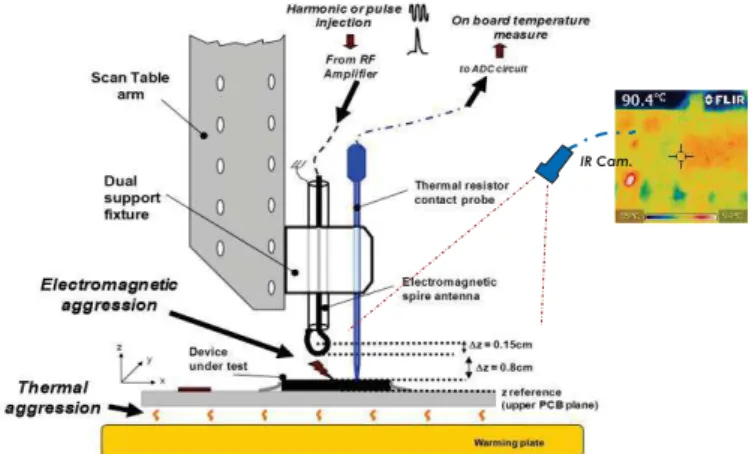
Separate E-Field and H-field measurement or injection, considered as Near-Field approach, are realized over different areas of PCB with dedicated probe's set like H-spires and E-dipoles, and associated to a motorized table system. Electromagnetic probes have been fabricated with high-frequency semi-rigid coaxial cable to inject RF power from MHz until 3GHz[11]. A warming plate, using inductive heating, is used to generate temperature until 300-350°C over a fixed glass area. It is placed under the PCB, with a specific conductive test support. A thermal contact probe, with a touch end of 0.1mm diameter, and a thin body support of 8cm long,
has been coupled on the same scan table moving fixture, with a different Z-axis reference, as seen in Erreur ! Source du
renvoi introuvable.. When moving, and positioning the
measurement point, thermal probe stays in with the body of the electric element, as near-field probes are just over.
Fig. 1. Schematic of the experimental dual thermal-near field set-up configuration for immunity testing on conventional PCB.
With this configuration, we can inject localized RF power at specific or sensitive area and wires of a PCB test, and relate it with the local real temperature of the injection zone. Some rigorous calibrations procedures must be completed before, because of the mutual influence of the EM probe and Thermal Probe. The warming plate can also modify the real level of injection of the probe. During the development of this set-up, we use a Microstrip receptor as a reference calibration. We observe that the shift in RF level injected can be about a maximum of 1.2 to 1.5 dB at high temperature. These discrepancies, between level injected from the generator and the victim, is used as a correction factor for a good validity of the experiment.
To complete the set-up, a IR-camera has been inserted, with a specific fixture, to have a 2D measurement of real temperature repartition on the PCB the EM and Thermal probes, and other elements in the flux of the heating [12].
B. TEM Cell aggression test bench
Transverse Electrical-Magnetic Cell (Crawford TEM cell) or GTEM (GHz TEM) are commonly used for EMC characterization, from MHz up to 10GHz, at PCB and Integrated Circuits levels [10][13][14]. As a well-suited alternative to large size experimental equipment for conventional radiated far field characterization, it allows very pertinent solutions for selective electromagnetic characterization of single electronic devices enclosed in the shielded cell environment. For this, special prototype of Printed Circuit Boards must be designed for the use in TEM cells, with the respect of three constraints: the dimension of the aperture of the cell, the completion of shielding quality of the system with a one-face metallic plane, and the choice of inside-components to be coupled with TEM Cell Septum in TEM modes.
Starting from this configuration, a special fixture arm has been realized, so to maintain both the PCB -TEM Cell device over the warming plate, at a height of 4cm, so to keep efficient heating action (Fig. 2). The new constraint is to place electrical and thermal connections very close to the PCB, and with 90° angle, so to avoid direct contact with the hot warming plate. Acquisition of real external temperature close on board is realized by thin thermal resistor in SMD or Thin Film technology. A special attention has been made, for pertinent immunity measurements, with the thermal routing network[11]. A specific roadmap procedure and computational algorithm has been developed to drive the experiment and all the post-processing data’s. As for the previous experiment, to refine the measurement of real temperature distribution all over the test board, the IR-camera system has been developed and inserted on this set-up. This improvement is especially helpful for TEM Cell characterization, both for calibration and to rely the different internal and external temperature on the PCB surface and on the TEM cell.
Fig. 2. 2D schematic of Heated TEM-Cell configuration for immunity testing on 10cmx10cm PCB.
III. APPLICATION ON PWM CIRCUIT BOARDS
A. Susceptibility tests on PWM patterns
Main applications of control boards concern the fine drive of power converter designed for well-suited motion or energy supply function [6], where high variation of temperature is clearly present. We want to focus on the more realistic EMC behavior of these circuits with non-ambient temperature environment. Some PCB prototypes have been designed for these studies, using either SMD chips reported on PCB, either Programmable Integrated Circuits type with Pulse Width Modulation pattern inside. PWM generators are controlled by cyclic rate input command.
Main susceptibility aspects are generally, for digital mode device, the drifts of thresholds levels and switching times, due to the couplings of external parasitic signals on supply and I/O ports[15]. Result of EM aggression show significant shifts in nominal characteristics of the output signal, in time domain. In consequence, the relative amplitude of waveform of current switching device, IVDD, has significant shifts with both
harmonic frequency and temperature aggression. The main significant effect is related to the potential shift of average signal during a PWM sequence, normally designed by the cyclic rate, so to drive current injection in power switches. So, IR Cam.
for our main immunity criteria, we choose to observe both discrepancies, in the frequency domain, with the survey of the spectrum waveform of the output switching current for example, and in time domain for main parameters as Duty cycle rate of the Output signal, as illustrate in Fig. 3 .
Fig. 3. Views of signal shifts on nominal PWM waveforms during harmonic aggression.
The EM aggression presented here have been realized in harmonic mode, using an Amplifier-RF source system. Power injection is realized from 1MHz to 3GHZ, with a maximum level of 40dBm. Susceptibility effect and Immunity test validation of the device are determined by the variations of the output signal: cyclic rate characteristics (time-domain, digital oscilloscope) and switching current frequency characteristics (frequency domain, spectrum analyzer), outside the range of default.
B. First demonstrator: Integrated PWM Circuit
The first study concerns a PCB with a PWM Integrated Circuit and electrical network up on one layer, which has been placed on dual thermal–EM near-field bench (Fig. 4). The level of supply is VDD=5V, provided by a high-speed current
switching voltage source, in respect with internal IC consumption time rate. Programmable circuit operates in synchronous mode, with a clock reference of 5MHz. Two inputs are used to modulate the output square signal, with an absolute cyclic rate from 5% to 46% (Input 2) and inversion mode (Input 3). Signal output is delivered on internal capacitance load (500fF) in parallel to external capacitance load(1pf).
Fig. 4. Upper view of the layer of the first PCB configuration
For our study, coupling the wave aggression impact with temperature, we look especially on the shift in frequency and amplitude of main peak of the current consumption spectrum: relative amplitude of waveform of current switching device, IVDD, is reported with significant harmonic frequency impact
couplings, at ambient temperature, in the 100 MHz-800MHz zone (Fig. 5). This variation is enforced when increasing, step by step, the external temperature and so the device package measured temperature. This indicates and confirms the modifications of switching current performances, and more significantly, an impact of high external temperature on electrical behavior of the programmable chip under electromagnetic pressure.
Fig. 5. Relative variation of switching amplitude of Integrated PWM circuit with dual thermal-harmonic wave aggressions
C. Second demonstrator: two discrete PWM circuits
The second study concerns a dual PWM generator, dedicated for driving independently two DC brushless motors. The two signals are realized with discrete SMD digital devices. The PCB is compliant with TEM Cell aperture (10cm*10cm) but the area of the overall circuit is about 3cm*3cm. The level Original PWM
Disturbed PWM
Original PWM Disturbed PWM
Temperature measurement points Electromagnetic aggression points
Supply line Ground line (return current) Clock1 input line CPLD 22v10 Package Clock2 input line TM_ Output line EA_ Warming zone TM1 TM2 TM3 TM4 EA1 EA2 EA3 -80 -60 -40 -20 0 0 200 400 600 800 1000 Frequency (MHz) Amp li tu d e ( d B µ V )
Amplitude Reference (no thermal-frequency constraint)
Temp. 22°C
of supply is VDD=5V. The nominal frequency of the two PWM
is f0=10kHz. Four main default's criteria are defined for these
test: the shift on duty cycle rate α, on frequency f0, on switching
margins VTOP- VBASE, and on the mean value VMEAN. TABLE I. PWM CRITERIA'S VALUES.
PWM parameter Nominal Value Range
Duty Cycle a min 27.42 % 24.67 % / 30.16 (10%) 27.14%/27.69%(1%) Duty Cycle a max 71,3 % 64.17 % / 78.43 (10%)
70.58%/72.01%(1%) VTOP 4.65 V 4.6V/4.69V VBASE 0.01 V -0.05V/+0.05V VMEAN (a min) 1,265V 1.25V/1.277V VMEAN (a max) 3.348V 3.31/3.38 Frequency 9.67 kHz 9.57kHz / 9.76kHz
This board has been tested with the TEM cell/thermal configuration, represented in Fig. 6. The two output signals, PWM00 and PWM01, have nominal characteristics at 20°: f0=10kHz, Vpp = 4.65V, a1= 71.3%, a2= 27.43%. A digital
wide-band and high sampling rate oscilloscope realizes the acquisition and the control of these parameters. Each default's criteria are tested independently, in the range of 10% to 1% of their nominal value (TABLE I. . Then, EM aggression is realized, by sweeping the frequency between 1MHz and 3GHz, and the levels of RF power from -40dBm to 40dBm.
Fig. 6. View of the heated TEM-Cell configuration for immunity testing.
The first step is to acquire a susceptibility figure at ambient temperature, when the warming plate is OFF. This first figure shows the susceptibility responses of our PCB, for the four criteria's chosen. A main common sensitive zone is depicted in the range of 300MHz-500MHz. At 600MHz, we have a specific susceptibility effect, with some criteria's as VMEAN that is less
sensitive to EM aggressions. This is due to coupling modes and resonances that are enforced in this range of frequency. This first test, realized at ambient temperature(20-22°C), is the reference susceptibility test presented in Fig. 7.
Fig. 7. Immunity table reference(20°C) for the four criterias: à duty cycle α £ frequency jitter Δ Switching margins • VMEAN
Then, in a second way, we repeat the experiment with steps of temperature of 20°. At About 90°, the shifts of PWM characteristics over 1% are continuously due to this temperature, because of the high impact of temperature on semi-conductor on the board. Among a wide number of parametric results, depending both of frequency, injection levels, temperature steps, and the kind of defaults, we present a synthetizes of the main significant results, with parametric Immunity figures as following
As the apparition of a default on the duty cycle with a maximum shift of 1% is critical for our applications, Fig. 8. is dedicated to this parameter. Compared to the reference measure at 20°C, it's significant that the levels of EM aggression for the “cyclic rate criteria” are lower of about 10 to 20 dB, in some narrow range of frequency, as 200 MHz, 700 MHz, and a minimum for all the temperature at 900MHz (GSM Band!)
Fig. 8. Immunity table at temperature steps of 20°C for criteria "1%" on duty cycle α
The second main result of these immunity investigation is presented in Fig. 9. This is a comparison of susceptibility effects at the worst case of thermal aggression, about 85°C, with IC still in normal activity. The effects of dual EM-Thermal
Warming plate TEM cell with PCB
( aperture down) Special "Thermos_IM" test fixture height screw adjustment Wideband generator Powermeter PWM pattern control system On-PCB temperature probe acquisition 0 5 10 15 20 25 30 35 40 0 200 400 600 800 1000 1200 A gr e ss io n L e v e l ( d B m) Frequency (MHz) 40°C 60°C 82°C
aggressions for both five criteria's of PWM susceptibility have been represented, in 3D-view, so to be compared: Duty@10%, Duty@1%, VTOP@1%, VBASE@1% and VMEAN@1%. Table I
resumes the criteria considered and the range of the nominal values controlled during dual electromagnetic-thermal aggressions.
This figure shows a real global shift of the sensitivity of the PCB and the PWM signals, at the maximum allowed temperature of test (85-90°) of the experiment. The previous sensitive zones are all enforced (280 MHz / 500 MHz/ 720 MHz/850Mhz), for all the criteria’s. Also, the most sensitive signal parameter at this temperature is the Mean Value (VMEAN)
of the PWM, which is unfortunately the worst case of integrity or robustness of the nominal specification of the PWM pattern for driving. Some narrow range of frequency becomes very sensitive and very weak (@250MHz), that indicates that the couplings of external RF Wave is maximum on the PCB, due to the action of temperature on both electrical resonances and shift of the Chip's impedances and switching margins.
Fig. 9. 3D table representation of worst-case's immunity with PCB temperature of 85°C, for 5 criterions of the PWM: Duty10%, Duty1%, Vtop1%, Vbase1%, Vmean1%
IV. CONCLUSIONS
With these works, new modified EMC characterization approach is in progress, for real-case EMC investigations. Specific test benches have been developed based on conventional Near-Field and TEM cell immunity test setups. External aggression of light range of temperature (20°-100°) has been correctly added, so to combine both EM-Thermal effects on susceptibility of electronic chips on PCB. The first test bench (Near-Field) is dedicated to conventional PCB, with the need of localized EM injection and temperature measurements, often on the component-face of the PCB. The second one, using a TEM cell, is dedicated for demonstrator PCB, where specific design and routing of chips and thermal sensors must be initially performed for the test. A focus has been made on immunity cases on PWM signals, which need to be well driven for main applications. After a measurement campaign that has produced a wide range of different
susceptibility responses of the demonstrators, main significant results are synthesized in this work. These parametric immunity cases for PCB boards confirm a main influence of temperature on susceptibility levels of programmable or discrete chips: some critical defaults, as the shift of more than 1% of the duty cycle rate or Mean value VMEAN, are very sensitive with a
non-ambient temperature, and critical for immunity of these applications.
With this review of thermal-immunity experimental study on PCB, some refinements and calibration progress of the two set-ups must be completed: the mutual influence on measurements and aggression of both TEM Cell, Near-Field probes and Thermal probes must be considered. In parallel, modeling investigations are also actually performed to try to understand and reproduce these effects of external temperature on EMC characteristics (emission, susceptibility) on electronic PCB, as already initiated for Emissions in [3]. With this modeling completion study, a first complete review of new EMC behavior cases dealing with new embedded and hybrid technology constraints will be validated, so to promote the merging of new concerns of EMC approach on electrical transport and embedded applications [5]
References
[1] J.M. Dienot, G. Lourdel, "Experimental study of thermal influence on EMC emission of digital circuit on PCB", Proceedings of the 16th International Symposium on Electromagnetic Compatibility, pp. 299-302, Zurich, February 13-18, 2005.
[2] S. Ben Dhia, E. Sicard, A. Boyer, Y. Mequignon, J.M. Dienot, " Thermal Influence on 16 bits Microcontroller Emission”, In Proc. of 2007 IEEE International Symposium on Electromagnetic Compatibility, EMC for IC session, Honolulu (USA), July 9-13, 2007.
[3] J.M. Dienot, "Characterization and simulation of digital device electromagnetic noise under non-ambient temperature conditions.", Electronics Letters Volume 43, Issue 20, pp 1073-1074, September, 2007, DOI 10.1049/el:20070495
[4] H. Boulzazen and al., "Experimental study and development of an “EMC-thermal stress” test bench used in Mode Stirred Reverberation Chamber “MSRC”"; In Proc. of 2009 International Workshop EMC'COMPO, Toulouse(FRA), November 17-19, 2009
[5] J.M. Dienot, E. Batista, "Real-Cases of Electromagnetic Immunity and Reliability in Embedded Electronics Architectures", in Book of Abstract of EUROEM 2012, pp 87, European Electromagnetic Symposium, Toulouse, France, 2-6 July, 2012.
[6] E. Hoene and al., "Simulating electromagnetic interactions in high power density converters", in Proc. of 36th IEEE Power Electronics Specialists Conference, pp. 1665-1670, Recife(BRA), 2005.
[7] S. Weber, S. Guttowski, E. Hoene, W. John and H. Reichl, " EMI Couplings from Automotive Traction Systems", In Proc. of IEEE Symposium on Electromagnetic Compatibility, Vol. 1, pp. 591-594 , Istanbul(TUR), May 11-16, 2003.
[8] D. Baudry, C. Arcambal, A. Louis, B. Mazari, and P. Eudeline, " Applications of the Near-Field Techniques in EMC Investigations", IEEE Trans. On Electromagnetic Compatibility, Vol. 49, N° 3, pp. 485-493, August 2007.
[9] K.P. Slattery, J. Neal, and W. Cui, "Near-field measurements of VLSI devices", IEEE Transactions on Electromagnetic Compatibility, vol.41, n°4, pp 374-384, November 1999.
[10] J.P. Muccioli, T.M. North and K.P. Slattery, "Investigations of the theoretical basis for using a 1 GHz TEM cell to evaluate the radiated emissions from integrated circuits", In Proc. IEEE EMC-S, Santa-Clara, pp. 63–67, August 1996.
VTOP1% DUTY1% VBASE1%
[11] J.M. Dienot, E. Batista and M. Bernard, "Dual experimental approach for thermal impacts on electromagnetic behavior of electronic circuit board configurations", IEEE Transactions on Instrumentation and Measurement, Volume 57, Number 11, pp 2405-2413, November, 2008. [12] A. Nguenche, "Mise en œuvre d'un système d'acquisition
thermographique 3D pour la caractérisation CEM Multi-physiques de modules électroniques", Rapport d'Etudes Labceem-UPS, Septembre 2016.
[13] P-M. Nicolae, I-D. Nicolae, D-G. Stănescu, "Using GTEM Cells for Immunity Tests on Electronic Boards with Microcontroller", In Proc. of IEEE 2012 Symposium on EMC, pp. 44 49, Pittsburgh(USA), August 5-10, 2012
[14] X. K. Gao, E. K. Chua, and E. P. Li, “Integrated EM immunity design and diagnosis system for electronic devices”, in Proc. of 2009 International Symposium on Electromagnetic Compatibility, pp. 329-332, Kyoto, Japan, July 20-24, 2009.
[15] H. Pues and C. Gazda, "A Black-Box Measurement-Based Modeling Method for the RF Emission and Immunity Behavior of ICs", in Proc. of IEEE International Symposium on Electromagnetic Compatibility and EMC Europe, EMC2015, pp. 1002-1006, ISBN 978-1-4799-6615-8.