S 1 Supplementary Information
Preferential Alignment of Incommensurate Block Copolymer Dot Arrays
Forming Moiré Superstructures
Cong Jin,†,‡
Brian C. Olsen,†,‡
Erik J. Luber,†,‡,*
& Jillian M. Buriak†,‡,
*
†. Department of Chemistry, University of Alberta, 11227 Saskatchewan Drive, Edmonton, AB T6G 2G2, Canada.
‡. National Institute for Nanotechnology, National Research Council Canada, 11421 Saskatchewan Drive, Edmonton, AB T6G 2M9, Canada.
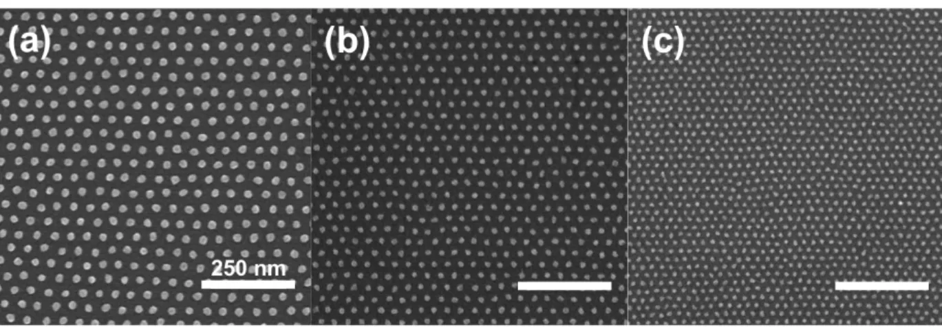
Figure S1. SEM micrographs of single layer silicon dot patterns converted from annealed (a)
B30, (b) P43, and (c) P22. All scale bars are 250 nm.
Figure S2. AFM micrographs of single layer silicon dot patterns converted from annealed (a)
S 3 Figure S3. Grain boundary of P43 (bottom) + B30 (top). (a) SEM micrograph of grain boundary
area. (b) FFT of white square area of (a). (c) Combined B30 (red dots) and P43 (blue dots). (d,e) Separated B30 and P43 arrays, respectively.
S 5 Figure S5. SEM micrographs (a, b), separated first layer pattern (e, d), second layer pattern (e,
f), combined double layer pattern (g, h) of B30 (bottom) + P43 (top) Moiré superstructure and
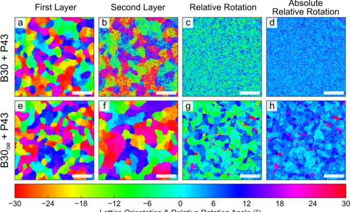
Figure S6. Dot pattern maps as described in Figure 5 for B30+P43 (a-d) and B30oe+P43 (e-h)
where the B30 was etched longer to decrease the particle size (B30oe). All scale bars are 5 μm in length.
S 7 Figure S7. ASH plots for RIE-treated dot heights obtained from AFM. (a) Dot height
distributions for single layers of P22, P43 and B30 (b) Dot height distributions for B30(bottom) + P43(top). Since the AFM tip was unable to reach the flat silicon substrate, dot heights were shifted to match the mean height of P43 from (c). The shoulder of the main peak in P43 is a consequence of taller B30 layer dot included in the P43 height distribution due to dot proximity.
(c) Dot height distributions for B30oe(bottom) + P43(top). The second peak of B30 is a