Analog VLSI Implementation of Synaptic Modification
in Realistic Neurons
by
Jason Leonard
Submitted to the Department of Electrical Engineering
and Computer Science in partial fulfillment of the
require-ments for the degrees of Bachelor of Science in Electrical
Science and Engineering and Master of Engineering in
Electrical Engineering and Computer Science
at the
MASSACHUSETTS INSTITUTE OF TECHNOLOGY
May 22, 1998
MAae \ \
© Jason Leonard, 1998. All Rights Reserved.
The author hereby grants to M.I.T. permission to
repro-duce and distribute publicly paper and electronic copies
of this thesis and to grant others the right to do so.
A uthor ...
...
...
Department of Electrical Engineerin~ and Computer Science
May 22, 1998
SSACHUSETTS INSTITUTE OF TECHNOLOGYJUN
1
6
1999
LIBRARIESCertified by ...
---...
.. ... o .Chi-Sang Poon
,-TWhsis Suvervisor
Accepted by ... .
...
Arthur C. Smith
Chairman, Department Committee on Graduate Theses
Analog VLSI Implementation of Synaptic Modification in
Realistic Neurons
by
Jason Leonard
Submitted to the Department of Electrical Engineering and Com-puter Science on May 22, 1998 in partial fulfillment of the
require-ments for the degrees of Bachelor of Science in Electrical Science and Engineering and Master of Engineering in Electrical
Engineer-ing and Computer Science
Abstract
An analog VLSI implementation of synaptic modification in realistic neurons is presented. The implementation uses CMOS integrated circuit technology to emulate the electrical behaviors of the neuron membrane, dendrite, and synapse, using principles based on the actual biology. The synapse circuitry includes a mechanism for the modification of the synaptic conductance. The circuits were simulated, layed out, and submitted for fabrica-tion.
Thesis Supervisor: Chi-Sang Poon
Title: Principal Research Scientist, Harvard-MIT Division of Health Sciences and Tech-nology
Table of Contents
1 Introduction ... 11 1.1 M otivation ... 11 1.2 B ackground ... ... 12 1.3 O bjective ... 12 2 Biological Background ... 13 2.1 O verview ... 132.2 Neuron Cell Body ... 13
2.3 Hebbian Synapse...15
3 A nalog V L SI ... 19
3.1 Subthreshold MOSFET Operation... ... ... 19
3.2 Basic Circuit Building Blocks ... 20
3.3 Follower Configurations ... 27
4 Circuit Implementation of Neuron Cell Body ... 31
4.1 Cell Membrane and Leakage Conductance ... 31
4.2 Potassium Ion Channel ... 32
4.3 Sodium Ion Channel ... 34
4.4 V oltage Scale ... ... 35
4.5 HSPICE Simulation ... ... 35
5 Circuit Implementation of Hebbian Synapse ... 39
5.1 NMDA Channel ... ... 39
5.2 Calcium Measurement ... 41
5.3 Threshold Detection ... 43
5.4 Non-NMDA Channel ... ... 45
5.5 Implementation of Time-varying Current...46
5.6 Digital Control Circuitry for Induction of LTP and LTD... 52
6 Circuit Implementation of Dendrite... 59
6.1 Polysilicon Resistor ... ... 59
6.2 Horizontal Resistor ... ... 60
6.3 Scaling C ircuitry ... 64
7 Simulation of Complete Neural Circuit ... 67
7.1 Simulation Setup ... 67
7.2 Simulation Results ... ... 67
8 Layout and Fabrication ... 73
8.1 Fabrication Technology ... 73
8.2 L ayout ... ... 73
8.3 Pin-out/Bonding Diagram... ... 74
8.4 T esting... ... 75
8.5 Estimated Layout Density... ... 75
9 C onclusion ... ... 77
9.1 Sum m ary ... ... 77
9.2 Future W ork ... ... 77
List of Figures
Figure 2.1: Electrical model of the nerve cell membrane ... 14
Figure 2.2: Electrical model of the spine head ... ... 16
Figure 3.1: D ifferential pair ... ... 20
Figure 3.2: Diode-connected configuration ... ... 21
Figure 3.3: Current m irrors ... ... 22
Figure 3.4: Simple transconductance amplifier... ... 23
Figure 3.5: Simulated output current of a simple transconductance amplifier ... 24
Figure 3.6: Wide output range transconductance amplifier... .... 25
Figure 3.7: Wide input range transconductance amplifier... .... 26
Figure 3.8: Follower configuration ... 27
Figure 3.9: Follower-integrator connection ... ... 28
Figure 4.1: Membrane capacitance and leakage conductance ... 31
Figure 4.2: Alternative circuit for membrane capacitance and leakage conductance...32
Figure 4.3: Circuit implementation of the potassium(IKD) ion current ... 33
Figure 4.4: Circuit implementation of the sodium ion current ... 34
Figure 4.5: Simulated step of input current into nerve membrane ... 36
Figure 4.6: Simulated response of nerve cell membrane voltage ... 36
Figure 5.1: Circuit Implementation of NMDA receptor channel ... 39
Figure 5.2: Peak NMDA current as a function of spine head voltage ... 41
Figure 5.2: Calcium concentration measurement circuit ... 42
Figure 5.3: Threshold detection circuit... ... 44
Figure 5.4: Circuit implementation of non-NMDA receptor channel ... 45
Figure 5.5: Peak non-NMDA current as a function of spine head voltage ... 47
Figure 5.6: Cascaded follower-integrators... .... ... ... 48
Figure 5.7: Buffered (digitized) action potentials... ... 49
Figure 5.8: Cascaded follower-integrators with leakage transistor ... 50
Figure 5.9: Alternative implementation of time-varying current... 51
Figure 5.10: NMDA current as a function of time... 51
Figure 5.11: non-NMDA current as a function of time... ... 52
Figure 5.12 Circuit implementation of simple LTP/LTD algorithm ... 54
Figure 5.11: Dependence of the change in conductance on calcium concentration ... 55
Figure 5.12 Block diagram of circuit implementation of LTP/LTD reversal algorithm 56 Figure 6.1: Horizontal resistor connection... ... ... 60
Figure 6.2: Biasing circuitry for horizontal resistor connection ... 61
Figure 6.3: Simulated current in the horizontal resistor as a function of bias voltage ...63
Figure 6.4: Simulated current in the horizontal resistor as a function of input voltage.. 64
Figure 6.5: Scaling circuitry ... ... ... ... 66
Figure 7.1: Presynaptic stimuli at 100 Hz...67
Figure 7.2: Nerve cell membrane voltage ... ... ... 68
Figure 7.3: N M D A current ... ... ... 68
Figure 7.4: Calcium concentration... ... ... ... 69
Figure 7.5: Calcium concentration and threshold detector output...69
Figure 7.7: Postsynaptic membrane potential ... ... 71
Figure 7.8: Postsynaptic membrane potential (LTP) ... .... 71
Figure 7.9: Change in non-NMDA conductance due to LTD ... 72
List of Tables
Table 2.1: Typical concentrations of ions in the nerve cell membrane ... 13
Table 5.1: Truth table for simple LTP/LTD algorithm ... 53
Table 5.2: Truth table for threshold logic of the LTP/LTD reversal algorithml ... 55
Chapter 1
Introduction 1.1 Motivation
Traditional electronic artificial networks implement mathematical or engineering abstrac-tions of biological neurons. These are usually designed using digital circuits that operate up to a million times faster than actual neurons. There is an interest, however, in develop-ing an artificial neural network that uses more life-like principles of neural computation. This type of neural network could potentially be used in electronic and electromechanical systems, such as artificial vision devices and robotic arms, to interact with real-world events in the same manner as biological nervous systems. This type of network could also be used as a research tool to better understand how biological neural networks communi-cate and learn. Today, the ability to simulate with software the behavior of biological net-works is severely limited. Considering that a biological nervous system contains thousands or millions of interconnected neurons, such simulations could take many hours or days on the fastest of computer. An electronic circuit that emulates the analog behavior of actual biological neurons could perform the simulation in real time.
1.2 Background
Most efforts[2],[4] at creating electronic implementations of biological neurons have focused on emulating the input-output functional characteristics of the neuron, essentially treating the neuron as an abstracted black box. These implementations focus on the creat-ing of an action potential, which is what neurons to communicate with one another, but with little regard for what actually produces the action potential in a biological neuron Mahowald and Douglas[1] have produced an analog integrated circuit with the functional characteristics of real nerve cells, but isomorphically emulates the membrane
conduc-tances within an actual neuron cell body.
1.3 Objective and Organization
This thesis discusses an analog VLSI implementation of a biological neuron. This imple-mentation builds on the work of Mahowald and Douglas, but adds circuitry for the synapse through which neurons communicate, and the dendrite, the connection between the syn-apse and neuron cell body. Also included is circuitry for adaptation, or learning.
Chapter 2 discusses the biology of the neuron and presents electrical models of the neuron cell body and a Hebbian synapse. Chapter 3 is an overview of analog VLSI tech-nology and discusses circuit blocks that are used in implementing the neuron circuits. Chapter 4 discusses in detail the implementation of the circuit for the neuron cell body,
based on the work of Mahowald and Douglas. Chapter 5 discusses the circuit
implementa-tion of the Hebbian synapse, including the circuitry for learning and adaptaimplementa-tion. Chapter 6 discusses the circuit implementation of the dendritic connection between the cell body and synapse. Chapter 8 presents HSPICE simulation results of a complete neural circuit. Chapter 9 discusses the layout in silicon of the circuits discussed in the previous chapters. Chapter 10 contains a summary of the results of this thesis, and offers suggestions for future work related to this thesis.
Chapter 2
Biological Background
2.1 Overview
The neuron is the basic anatomical unit of the nervous system[4]. It consists of a cell body equipped with a tree of filamentary structures called dendrites. The dendrites are covered with structures called synapses, where junctions are formed with other neurons. The syn-apses are the primary information processing elements in neural systems. The dendrites sum the synaptic inputs from other neurons, and the resulting currents are integrated on the membrane capacitance of the cell body until a threshold is reached. At that point, an output nerve pulse, called the action potential, is generated and then propagates down the neuron's axon, a long structure used to transmit data. The end of the axon consists of a tree of synaptic contacts that connect to the dendrites of other neurons.
2.2 Neuron Cell Body
The electrical activity in a neuron cell body occurs in the thin membrane that electrically
Concentration Concentration Reverse Potential
Ion
Inside (mM/1) Outside (mM/1) (mV)
Potassium (K+) 400 10 -92
Sodium (Na+) 50 460 55
Chlorine (Cl-) 40 540 -65
Table 2.1: Typical concentrations of ions in the nerve cell membrane[4]
separates the neuron's interior from exterior fluid. An energy barrier is formed by the nerve membrane that is so high that few ions are able to surmount it[4]. Inside all nerve membranes are metabolic pumps that actively expel sodium ions from the cytoplasm while importing potassium ions from the extracellular fluid. The concentrations of these
ions inside and outside the cell are shown in Table 2.1.
The concentration gradient that exists across the membrane is used to power electrical activity. Ions diffuse in(out) of the membrane while electrically drifting out(in). When the voltage across the membrane reaches the reverse potential
kT Nin
Vr = -kIn- , (2.1)
q Nex
the diffusion of ions will be exactly counterbalanced by the drift of ions. The reverse potentials for the three ions in the membrane are shown in Table 2.1. In operational terms, one can think of the sodium reverse potential as a positive power supply rail and the potas-sium reverse potential as the negative rail[4].
gK gNa gC1
men
EK E Na EC1
Figure 2.1: Electrical Model of Nerve Cell Membrane
Figure 2.1 summarizes the electrical characteristics of the nerve membrane. The volt-age sources represent the reverse potentials of the ions, while the conductances represent the membrane permeability for that ion. The membrane capacitance is depicted as a lumped capacitor. For a given membrane voltage, the current through the membrane(i.e., the capacitor current) is
Imem = (VmemK - VK)GK + (VNa - Vmem)GNa + (VcI - Vmem)Gci (2.2)
Any net current will charge or discharge the membrane capacitance until the current is reduced to zero. Under normal conditions, the chlorine current is small and can be
neglected[4]. With this assumption, the voltage at which the net current is zero is:
VKGK + VNaGNa (2.3)
V = (2.3)
GK + GNa
VO is called the resting potential and is typically equal to -85 millivolts, although it can
vary considerably. A neuron at rest is termed "polarized" to a negative potential. The membrane becomes depolarized when its potential becomes more positive.
There are actually a number of different potassium ion currents. The delayed rectifier current, IKD, along with the sodium current, generates the nerve impulse. Two other potassium currents with slower dynamics, the so-called A-current(IKA) and the calcium dependent potassium current (IAHP or after-hyperpolarizing current), control the rate at which impulses are produced[1].
The activation and inactivation of the ion conductances in the membrane are them-selves dependent on the membrane voltage and time. There is a sigmoidal relationship between the ion conductance and the membrane voltage. This creates a thresholding behavior that is responsible for the generation of the nerve pulse, or action potential. As the membrane becomes depolarized(in response to, for instance, an influx of synaptic cur-rent), there is a transient the sodium conductance, followed by a delayed but prolonged increase in the potassium conductance. The currents through these conductances create the action potential by acting on the capacitance of the membrane.
2.3 Hebbian Synapse
The model presented here is that proposed by Zador, Koch, and Brown[6]. Stimulation of the presynaptic neuron causes the release of neurotransmitters from its axon terminal. These transmitters include the amino acid glutamate.The transmitters bind to correspond-ing receptors on the postsynaptic membrane, causcorrespond-ing ion channels to open up through these receptors. Glutamate binds to three types of receptors: n-methyl-D-aspartate
(NMDA), quisqualate, and kainate. LTP and LTD[3] are both mediated by the NMDA
receptors, which carry primarily Ca2+ currents. The other receptors, termed the
non-NMDA receptors, carry the rest of the synaptic current, consisting mainly of Na+, with
negligible Ca2+ content. These receptors are located on a spine head connected to the
den-dritic shaft.
h non nmd
Ch
Eh non Enmda
Figure 2.2: Electrical Model of the Spine Head
Figure 2.2 depicts the electrical model of the spine head. The total synaptic current consists of the sum of the NMDA and non-NMDA currents. There also exists a small leak-age conductance and the capacitance that represents the membrane capacitance of the spine head. The current through the non-NMDA channels in response to a presynaptic stimulus is given by an alpha function:
Ino n = (Enon - Vhead)( Kgpte Pt (2.4)
where K = e/tp, e is the base of the natural logarithm, tp = 1.5ms, g = 0.5nS, and
Enon = 0 .Note that the non-NMDA receptor conductance is purely
ligand(neurotransmit-ter) dependent. The NMDA conductance, on the other hand, is both ligand dependent, due to the binding of neurotransmitters released from the presynaptic neuron, and dependent on the spine head membrane voltage. The current through the NMDA receptors is given by:
et -t
INMDA(t) = (ENMDA - Vhead)gn 2+ - ea (2.5) 1+ n[Mg2 + ]e head
where c, = 80ms, T2 = 0.67ms, rI = 0.33nM-1, y = 0.06mV'-, ENMDA = 0, and g = 0.2nS. The voltage dependence of the NMDA receptor arises from the fact that the receptors
inhibited by Mg2+ ions whose binding rate constant is dependent on the spine head
mem-brane voltage. Near the resting memmem-brane potential, the NMDA receptor channels are
almost completely blocked by the Mg2+ ions, and thus little current flows. As the spine
head membrane becomes partially depolarized, the Mg2+ ions become dislodged and more
NMDA current flows.
The postsynaptic flow of Ca2+ ions through the NMDA receptor channels is crucial for
the induction of LTP and LTD[3]. Upon entering the dendritic spine, the Ca2+ ions trigger
a series of events that lead to the induction and maintenance of LTP or LTD. The precise mechanisms, however, are not well understood. One theory is that a second messenger,
such as nitric oxide, is activated by the Ca2+ ions and certain calcium dependent proteins
and then diffuses back to the presynaptic terminal, stimulating the release of more glutamate. Thus, this retrograde messenger operates as a positive feedback mechanism. This model is limited, though, in that it would only explain LTP. Another model suggests that rather than affecting presynaptic neurotransmitter release, the induction of LTP or LTD modulates the postsynaptic conductance of the non-NMDA receptor channels, which
carry the bulk of synaptic current[3]. This model also relies on the influx of Ca2+ ions into
the dendritic spines through the NMDA channel. During high frequency stimulation, the
Ca2+ ions reach high concentrations in the compartmentalized spine head and
preferen-tially activates a protein kinase. During low frequency stimulation, lower concentrations are reached and a protein phosphatase is released. Both proteins act on a common
phos-phoprotein, which triggers LTP or LTD by modulating the non-NMDA receptor channel conductance.
Chapter 3
Analog VLSI
This chapter discusses the analog circuits that are used as building blocks in the imple-mentation of the neuron circuits. First, the principles of subthreshold behavior of CMOS transistors are discussed. Then, the circuit building blocks are discussed in detail.
3.1 Subthreshold MOSFET Operation
In traditional analog CMOS circuits, the transistors are biased in the saturation, or strong inversion, region of operation, where the drain current is given by
los = k (VGS- Vt)2(1 +. VDs) (3.1)
where k' is a physical parameter, W/L is the ratio of the transistor channel width to channel
length, VGS is the gate-to-source voltage, Vt is the threshold voltage of the transistor, X is
the inverse of the Early voltage of the transistor, a parameter related to the output
resis-tance of the device, and VDS is the drain-to-source voltage.For VD(os),> 1, the current is
roughly independent of the drain-to-source voltage.
Generally, the transistor is not used in the subthreshold, or weak inversion, region of operation. In this region, the current levels are very small and the drain current varies exponentially with the gate voltage:
IDS= kxenV( - e v (3.2)
where kx and n are fabrication dependent parameters and VT is the thermal voltage, which
is approximately 26 millivolts at room temperature. For drain-to-source voltages greater than a few thermal voltages, the drain current is essentially independent of the drain-to-source voltage.
Most of the circuits discussed in this thesis have transistors biased in the subthreshold region, to take advantage of the exponential relationship between current and voltage, which is prevalent in actual neurons. CMOS technology is used instead of bipolar
technol-ogy because of the greater availability of CMOS processes. Also, the current levels, and hence time scales, of subthreshold CMOS transistors match up fairly well with the actual biological levels. Additionally, the nearly infinite resistance of the MOS gate is useful in many circuits.
3.2 Basic Circuit Building Blocks
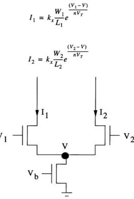
3.2.1 Differential Pair
Perhaps the most important circuit is the differential pair shown in Figure 3.1. Assum-ing large enough drain-to-source voltages, the currents I, and 12 can be expressed as
(VI - V) W1 V(, I = kx, e vT (3.3) L, (V2 - V) W2 nVT 12 = kx 2e
VI
d
(3.4) V2 VbFigure 3.1: Differential Pair
These sum of these two drain currents must be equal to the current Ib through the bias tran-sistor:
Solving this equation for the node voltage V yields:
-V V, V2
nV, /W1 +
W2
Ib = I + 2 = kxe nT e n + e
(II L2
-V ev--, Ib 1 e VT =- (3.6) k v, V2 x Wl ny, W2 nV, L( L2
Substituting Equation 3.6 into Equations 3.3 and 3.4 yields expressions for the drain cur-rents: V1 -e L1 (3.7) I1 = Ib Vl V2 (3.7) W1 n , W2 nV, -e +--e L, L2 VI W2 nV, +-e L2 12 = Ib
Wl
Vl V2 (3.8) nyTW2
nV, LI L2 eEssentially, if V1 is more positive than V2 by many n VT, the voltage V rises to turn
transis-tor M2 off, so that all of the current goes through Ml and I, = Ib .The analogous situation
occurs when V2 is more positive than V1.
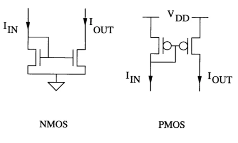
3.2.2 Current Mirror
Figure 3.2: Diode-connected configuration for NMOS and PMOS devices
Figure 3.2 depicts the diode-connected circuit configuration, where the transistor's gate is connected to its drain. Thus, VGS =VDS, which for all useful gate-to-sources volt-ages means that the VDS term in Equation 3.2 is negligible, guaranteeing that the transistor is saturated.
I 1
IIN OUT
IIN 'OUT
NMOS PMOS
Figure 3.3: Current Mirrors
The circuits shown in Figure 3.3 are NMOS and PMOS current mirrors. In the NMOS current mirror, transistor Ml is diode-connected, and its gate is also connected to the gate of M2. Since the sources of M1 and M2 are common, they both have the same VGS. Hence, assuming that the VDS. of M2 is large enough for M2 to be saturated also, the
cur-rent IOUT is:
W2/L 2
oUr W-1l (3.9)
Thus, the current mirror not only "mirrors" the input current, but it can scale it also.
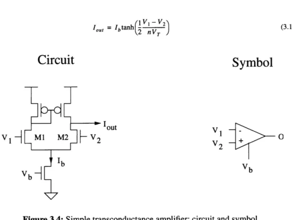
3.2.3 Transconductance Amplifier
The simple transconductance amplifier[4] is shown in Figure 3.4. It consists of a dif-ferential pair "loaded" with a PMOS current mirror. If the transistors in the PMOS current mirror have the same dimensions, then the current I, is mirrored with unity gain to the other leg of the current mirror. Assuming that the transistors Ml and M2 of the differential pair are matched; i.e., the have the same W/L ratio, then the output current can be expressed as: V, V2 nVT nV, e -e Iout = 11 - 2 = Ib V1 V2 nVT nVT e +e
lout = Ibtanh(1 V, - V (3.10) (,2 nV)
Circuit
Symbol
out V -V M1 M2-V
2 V1 -Vb b VbFigure 3.4: Simple transconductance amplifier: circuit and symbol
The output current is plotted as a function of V1-V2 in Figure 3.5 for n=?. Note that the
output current is approximately linearly dependent on the input voltage difference for dif-ferences up to 100 millivolts, after which the output current begins to saturate to positive
or negative Ib .
Figure 3.5: Output current of a simple transconductance amplifier as a function of the
dif-ference in input voltages. Vb=? n=?.
The transconductance of the simple transconductance amplifier in this linear region,
with Vin defined to be V1 - V2, is
Iout 1 Ib
gM out _ (3.11)
"' aVin 2nV,
and is proportional to the bias current Ib.
A - out
A = ut gmrout (3.12)
where rout is the finite output resistance of the amplifier. This is an effect of the
devia-tion from ideal current source behavior of the amplifier. rout is defined as:
aVout
rout - out (3.13)
ot out
and can be expressed as:
rout = roN II rop = II (3.14)
where roN and rop are the incremental output resistances of M2 and M4, respectively, and VN and Vp are the Early voltages of NMOS and PMOS transistors, respectively. The Early voltages are proportional to channel length. Thus, the incremental voltage gain A of the amplifier is[4]
1 1 1
A = + - (3.15)
nV, V, V,
One of the limitations of this simple transconductance amplifier is that its output volt-age can has a significant lower limit. In other words, the output voltvolt-age cannot decrease below a certain value and the amplifier still work as desired. That critical value is:
Vout-min -= (min(V1, V2)- Vb) (3.16)
n
Essentially, the amplifier will work as desired with its output voltage almost up to the power supply VDD and down to Vb below the lowest input voltage. The fact that this lower bound depends on the input voltage limits the useful applications of the circuit.
3.2.4 Wide Output Range Amplifier
The circuit in Figure 3.6 avoids the output voltage limitation of the simple transcon-ductance amplifier discussed in Section 3.2.3. This output of this circuit is capable of swinging almost down to ground and almost up to VDD, independent of the input voltages.
Figure 3.6: Wide output range transconductance amplifier schematic
The current through M1 is mirrored through M3 and M4, while the current through M2 is mirrored through M5 and M6, and then again through M7 and M8. The currents flowing through M4 and M8 are just the two currents in the differential pair. the output current, then, is just the difference between I1 and 12.
The diode-connect transistors M3, M5, and M7 hold the drains of Ml, M2, and M6, respectively, relatively constant.Hence, the output resistances of these transistors are not crucial to the operation of this circuit. Only the drain to source voltages of transistors Mb, M4 and M8 operate over a large range in this circuit. The channel lengths of these transis-tors can be made long to increase their output resistances, and therefore make the output currents of this circuit largely independent of the output voltage. The high output resis-tances of M4 and M8 also give the circuit a large voltage gain.
3.2.5 Wide Input Range Amplifier
In some applications, it is necessary for the transconductance amplifier to approximate a linear conductance over a range larger than the approximately 100 millivolts of the sim-ple amplifier discussed in section 3.2.3. The amplifier shown in Figure 3.7 has a linear range twice that of the simple transconductance amplifier. This amplifier has a diode-con-nected transistor in each of the legs of the differential pair. Consider the currents in each
leg of the differential pair. II and 12 can be expressed as
S= (V - VA)/(nV) = (VA - VN)/(nV,) (3.17)
12 =I0e (V2- VB)/(nVT) = (VB- VN)/(nV) (3.18)
Solving for VA and VB,
(-2VA)/(nV) (-VN)/(nV,) (-V,)/(nVT) (3.19)
e = e e (3.19)
(-2VB)/(nV) (-VN)/(nV,) -(V2)/(nVr)
(-VA)/(nVT) (-VN)/( 2nVT) (-V)/(2nVT) e = e e (-VB)/(n V) e =- e-VN)/( 2 nVT) (-V 2)/(2nV,) e V 1
Figure 3.7: Wide input range transconductance amplifier
Noting that the currents I, and 12 must sum to the bias current Ib ,
Ib = + 12 = (-VN)/(nVT) (eV/(nVT) eV/(nVrT) I= b Ioe(- nV2 = oe (e + e ) (-VN)/(n V,) V/(n V,) Vl/(2nVT) V/(n VT) V2/(2n VT) Ib =Oe (e e +e e ) (3.23) (3.24) (3.25) (3.26) Ib = loe(-VN)/(2nVT) (eV/(2nVT) + eV2/(2nVT) (-VN)/( 2nV) Ib 1 e (e V /(2nV) + eV2/( 2 nV)) Io(e (2lV + e )
Plugging Equations 3.20-21 and 3.26 into Equations 3.17-18, we get expressions for 11 and 12 in terms of V1 and V2:
V1/(2nV,) e 1 =b Vl/( 2nVT) V2/(2nVT)) (e +e ) V2/(2nV,) e 2 = Ib V,/(2nV) V 2/(2nVT) (e + e
)
From these expressions, we can write the output current as
(3.27)
(3.28) (3.21) (3.22)
lout = II1-12 = Ibtanh V,- (3.29)
This is of the same for as the output current for the simple transconductance amplifier. However, the argument of the hyperbolic tangent function contains an additional factor of one-half. Hence, the input voltage difference can be twice as large for this amplifier as the simple transconductance amplifier and still maintain an approximately linear conductance.
3.3 Follower Configurations
3.3.1 Voltage Follower
The unity-gain voltage follower, or buffer, configuration is shown in Figure 3.8. The output voltage follows changes in the input voltage, without affecting the circuit produc-ing the input. The output voltage of the amplifier is the voltage gain of the amplifier multi-plied by the difference in the voltages at its input terminals:
Vout = A(Vin- Vout) (3.30) Hence the transfer function of the amplifier is:
V out- 1 1
1 (3.31)
Vin 1 + A
which for large values of A is close to 1. The simple transconductance amplifier can achieve gains on the order of 100-200, while the wide output range amplifier can achieve a gain of over 1000. Determining which amplifier to use, including whether to use a tradi-tional operatradi-tional amplifier, depends on the application and the desired accuracy
V - Vout
Vb
3.3.2 Follower-Integrator
The follower-integrator connection is shown in Figure 3.9. It contains an amplifier of
the types discussed in Sections 3.2.3-5 connected as a follower, with a capacitor connected
between the amplifier's output and ground. The output voltage can be described by the dif-ferential equation
C-dV = Ibtanh Vin - Vout(3.32)
dt 2nVT (3.32)
Vin V out
Vb
Figure 3.9: Follower-integrator connection
When the argument of the tanh function is small enough so that it is approximately lin-early dependent on its input, the differential equation becomes
dVout
C- = gm(Vi, - V,,,) (3.33)
where the conductance gm is defined as in Equation 3.11. This is a first-order differential equation analogous to that of an RC circuit in which a voltage source drives a series com-bination of a resistor and a capacitor.In the circuit shown here, the conductance of the transconductance amplifier corresponds to the resistor in the RC circuit. The transfer func-tion of this circuit, using frequency domain notafunc-tion(i.e., Laplace transform), can be expressed as
Vout out 1 (3.34)
Vin 1 + st
this circuit to a small (small enough so that we may assume the tanh function is approxi-mately linear) step change can be expressed as
Vou,(t) = Vouto (0) + AVi(1 - e- t/ ) (3.35)
Since the follower-integrator connection has an infinite input resistance, multiple fol-lower-integrators can be cascaded without loading one another, which is not true of a pas-sive RC network. Thus, the circuit can be cascaded to form a delay line whose transfer function and delay is well prescribed. Furthermore, the time constant of the follower-inte-grator connection can be varied over orders of magnitude by varying the bias voltage of the transconductance amplifier.
Chapter 4
Circuit Implementation of Nerve Cell Membrane
This chapter discusses the implementation of the electrical model of the nerve cell membrane shown in Figure 2.1. All circuits in this section and throughout the thesis were implemented using the parameters of the Orbit 2.0 micron fabrication process. Device
sizes and bias voltages were chosen based on this process.
4.1 Cell Membrane and Leakage Conductance
The cell membrane capacitance shown in Figure 2.1 is implemented with a real capacitor, connected between the 'membrane' node and ground, whose structure is discussed in Chapter 8:Layout and Fabrication. The value of this capacitance is approximately 1 pico-farad. There is also a leakage conductance (not shown in Figure 2.1) in the nerve cell membrane. The value of this conductance can be treated as constant.
SVmem V
0
V leak
Figure 4.1: Membrane capacitance and leakage conductance(implemented using a
transconductance amplifier).
This leakage conductance can be implemented using a transconductance amplifier connected in a follower-integrator configuration, with the output voltage being the mem-brane voltage and the capacitor being the memmem-brane capacitance[5], as shown in Figure 4.1. The input voltage of the amplifier should be the resting potential voltage(Equation.
2.3), since there is no leakage current when the membrane voltage is at the rest resting potential. The value of the leakage conductance is determined by the bias voltage of the transconductance amplifier, which determines its gm. The use of a transconductance amplifier yields a good approximation of the linear conductance. To improve the range over which there is an approximately constant conductance, the wide input range
transconductance amplifier of Section 3.2.5 can be used instead of the simple
transconduc-tance amplifier.
V mem
leak-Figure 4.2: Membrane capacitance and leakage conductance(implemented using a single
transistor)
Alternately, the leakage conductance can be implemented using a single transistor, whose gate voltage is set to control the leakage current[2], as shown(with the membrane capacitor) in Figure 4.2. This implementation does not emulate a true conductance how-ever, as the current through the transistor does not vary, to first order, with its drain to source voltage. Nonetheless, since the leakage current is relatively small, the loss of accu-racy comes with the benefit of a very simple and small implementation with a single
tran-sistor.
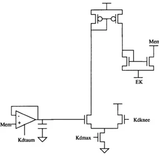
4.2 Potassium Ion Channel
Figure 4.3 depicts the circuits used to generate the delayed rectifier potassium current (IKD). This is the topology developed by Mahowald and Douglas[1]. This topology was implemented using the parameters of the Orbit 2.0 micron fabrication process. Device sizes and bias voltages were chosen based on this process.
The membrane voltage is delayed(low-pass filtered) by a follower-integrator, whose output voltage is compared to a reference voltage KDKNEE of a differential pair. The cur-rent flowing out of the diffecur-rential pair is mirrored by a PMOS curcur-rent mirror into a NMOS 'conductance' transistor, whose source is connected to the power supply voltage EK(corresponding to the potassium reverse potential in Figure 2.1) and whose drain is connected to the membrane node. The conductance transistor is designed with dimensions that make its behavior more ohmic than typical CMOS transistor, although the ohmic behavior is far from ideal. This transistor sinks current from the membrane capacitance.
7
Mem
EK
Mem + Kdknee
Kdtaum Kdmax
Figure 4.3: Circuit implementation of the potassium(IKD) ion current in the cell
mem-brane.
The voltage dependence of the potassium conductance is provided by the differential pair, which Mahowald and Douglas refer to as the activation transistors. The potassium current IKD does not become inactivated, unlike the sodium current, and thus does not require an inactivation signal, as will be seen in the following section for the sodium con-ductance.The time dependence of the conductance is provided by the follower-integrator, whose time constant is determined by a fixed capacitor(of value 1 picofarad) and the
vari-able bias voltage KDTAUM of the transconductance amplifier. The voltage KDMAX con-trols the maximum amount of current that flows in the differential pair.
4.3 Sodium Ion Channel
The circuits used to generate the sodium ion current in the cell membrane are shown in Figure 4.4. Unlike the potassium current IKD, the sodium current depends on the interac-tion of activainterac-tion and inactivainterac-tion circuits.
The sodium current activates very quickly, so there is no need for a follower-integrator to delay the membrane voltage signal to the activation differential pair. The output current from the activation subcircuit represents sodium activation. The inactivation of sodium is delayed, so the low-pass filtered version of the membrane voltage is applied to the input of the inactivation differential pair. The output current of this differential pair, representing the sodium inactivation current is then mirrored by the PMOS current mirror.
A straightforward application of Kirchoff's Current Law at the node NAVG yields
INAVG - activation linactivation (4.1)
This current is then mirrored to a conductance transistor, connected between ENA and the membrane node. ENA represents the sodium reverse potential shown in Figure 2.1.
ENA
Mem
Mem aNMf
M
NaonkneeM
Naonmax-] Naoffmaxl Natauh
Figure 4.4: Circuit implementation of the sodium ion conductance in the nerve cell mem-brane.
maxi-mum amount of current that flows in the activation and inactivation subcircuits, respec-tively.
4.4 Voltage Scale
The nerve cell membrane voltage can vary between the limits set by the reverse potentials of potassium(EK) and sodium(ENA). In real neurons, these limits are approximately -100 millivolts and +50 millivolts, respectively. Biological conductances are roughly ten times as sensitive to voltage as CMOS transistors[l]. Furthermore, the circuits discussed in the previous sections are driven by a 0-5 Volt power supply for the Orbit 2.0 micron process transistors. For convenience, the circuit or electronic reverse ion potentials are set to EK =
1.5 V and ENA = 3.0 V. In other words,
Velectronic = l1Vbiological + 2.5V (4.2)
This choice of voltage provides 10 times as large a range of membrane voltage and is half-way between the power supply and ground.
4.5 HSPICE Simulation of Nerve Membrane Circuits
Figures 4.5 and 4.6 show the results of an HSPICE simulation of the nerve cell membrane circuits using the Orbit 2.0 micron fabrication process parameters. In this simulation, the only ion conductances that are included are the sodium and potassium(IKD) currents.
A step of excitory (synaptic) current is injected into the nerve cell membrane, as shown in the schematic of Figure 4.5. This stimulus and the response of the neuron cell membrane are shown in Figure 4.6. The voltage on the membrane capacitor builds up as the input current dumps charge onto it. Once the membrane voltage reaches a certain value, the sodium activation circuit is activated. This circuit rapidly injects current into the membrane capacitor, causing its voltage to rise rapidly. Soon afterward the potassium cur-rent and the sodium inactivation curcur-rent start conducting. The sodium inactivation cancels
0 50 100 150
time (milliseconds)
200 250 300
Figure 4.5: Step of input current into nerve membrane
out the sodium activation, while the potassium current drains current from the membrane capacitor, rapidly decreasing its voltage, and effectively deactivating the sodium and potassium circuits. Thus, the nerve impulse is created. Since in this simulation the excitory
50 100 150
time (milliseconds)
200 250 300
Figure 4.6: Nerve cell membrane voltage in response to step in input current stimulus is a constant step in current, the membrane voltage again begins to build up and eventually another nerve impulse is created. In this simulation, the frequency with which
UU 450 400 350 E c300 250 200 150 100 50 0 S2.5 0, C 0 E 0 .QE 2 2 0) z 1.5 0 ' I "' I a. v I i --- iI
j/
the nerve impulses are created is dependent upon the value of the step in input current, the size of the membrane capacitance, and the conductances of the sodium and potassium ion channels.
Chapter
5
Circuit Implementation of a Hebbian Synapse
5.1 NMDA Channel
The circuit implementation of the NMDA receptor channel is shown in Figure 5.1. Recall from Equation 2.5 that the conductance of the NMDA channel not only varies with time, but is also dependent on the spine head membrane voltage. This functional dependence on voltage is implemented using the differential pair in Figure 5.1. Applying and rearranging the Equation 3.7to this differential pair yields:
1
'diffpair = I(t) VRe-VHead (5.1)
nVT
1 + Ze
where Z is the ratio of the sizes of the transistors in the two legs of the differential pair.
Ref - k Head
to c
ciH
Head
Headd
Idiffpair then serves as the bias current for the transconductance amplifier. Assuming the transconductance amplifier is operating in its linear range, its output current is
I1d iff pai r
iout-amp = (VHead- VRef)g m = (VHead- VRef) nff (5.2)
2 nVT
This current is then mirrored(with appropriate scaling) through the PMOS current mirror back to the spine head membrane (and also to the calcium concentration circuit described
in Section 5.2). If I(t) is chosen appropriately, then Equation 5.2 will have the same form
as described in Equation 2.2. The actual implementation of I(t) will be discussed in
Sec-tion 5.5.
In order to maintain the proper exponential dependence on voltage in implementing
Equation 2.2 with the circuit in Figure 5.1, whose voltage dependence is described by
Equation 5.1, It is necessary to shift and scale the voltage ranges over which the circuits operate, just as was described in Chapter 4 when implementing the neuron cell body. However, in this case the voltage scaling will be different.
Typically, the spine head voltage varies between -80 mV and 0 mV[6]. For conve-nience, the biological 0 V is again chosen to be 2.5 V. Thus, there is a 2.5 V shift between an actual biological channel and the electronic implementation. The voltage range must also be scaled to maintain the same behavior in the exponential. From Equations 2.2 and 5.1, it is apparent that
Y = x (5.3)
nVT
where x is the ratio of the electronic implementation voltage to the actual biological volt-age. For typical values of n, x should be approximately 2. In other words, while the biolog-ical voltage changes over a range of approximately 80 mV, the actual implementation will vary range over 160 mV. Formally, the voltages are related according to:
Velectronic = 2Vbiological + 2.5V (5.4)
Thus, the spine head voltage, in the electronic implementation, will vary from
approxi-mately 2.34 V to 2.5 V. This implies that VRef in Figure 5.1 should equal 2.5 V. Also, since
the differential input of the transconductance amplifier is potentially up to 160 mV, greater
than the linear range of the simple transconductance amplifier, it is best to replace the sim-ple transconductance amplifier with one with a wide input range, as discussed in Section 3.2.5, which has a linear range of nearly 200 mV.
NMDA Current-Voltage (Conductance) Relationship 250 200 E
8
S150 C 100 50 50 2.34 2.34 2.36 2.38 2.4 2.42 2.44 2.46 2.48 2.5Spine Head Voltage (Volts)
The voltage dependence of NMDA current produced by the circuits in Figure 5.1 is
shown in Figure 5.2. Here, the peak current is plotted as a function of voltage. For lower
vales of the spine head voltage, corresponding to negative highly polarized values of bio-logical potential, the magnesium ions block the NMDA channel and the current is small. As the spine head becomes depolarized (to a more positive potential), the NMDA channel conducts more. When the spine head voltage gets very close to its resting potential(biolog-ical = 0 mV; electronic = 2.5 V) very little current flows because the voltage gradient is small.
5.2
Calcium Measurement
Ref
-from NMDA + - Rest
circuit
Leak
Figure 5.3: Calcium concentration measurement circuit
The circuit in Figure 5.2 measures the concentration of Ca2+ ions in the
compartmental-ized spine head. Recall from Section 2.3 that these ions are the impetus for the induction
of LTP or LTD. The Ca2+ ions enter the spine head primarily from the NMDA channel
current, which mostly consists of Ca2+ ions. Thus, the flow of Ca2+ ions into the spine
head is roughly proportional to the NMDA current. Hence, a fairly accurate measure of the
Ca2+ concentration in the spine head is the measure of net charge over time that flows in
Q(t2)-Q(tl) = I(t)dt. (5.5) This charge can be accumulated on a capacitor, whose voltage is thus proportional to the
charge. In other words, the concentration of Ca2+ ions can be measured by accumulating a
scaled copy of the NMDA current onto a capacitor. The voltage on the capacitor will then
represent the concentration of Ca2+ ions. This is implemented in the circuit in Figure 5.2.
The NMDA current is mirrored and scaled by the PMOS current mirror. This current then is accumulated onto a capacitor connected to ground. The voltage on the capacitor can be expressed as
V 2+ (t) = INMDA(t)dt + V Ca2+ (0). (5.6)
Also shown in the figure is a transconductance amplifier connected in the follower configuration with its output connected to one terminal of the capacitor. This provides for a leakage current, whose time constant is determined by the gm (and thus is controllable by modifying the bias voltage) of the amplifier and the capacitance of the capacitor. The volt-age VRest determines the resting level of the capacitor voltvolt-age when there is not current flowing onto it(and none leaking off)
5.3
Threshold Detection
When the concentration of Ca2+ ions in the spine head reaches certain levels, LTP or LTP
may be triggered. Thus, it is desirable to have some type of threshold detection to
deter-mine when VCa2+ has crossed certain voltage levels. Thus, a circuit of the type shown in
Figure 5.4 is desired. Each comparator compares VCa2+ to a reference voltage and
pro-duces a digital 1 if VCa2+ is greater than the reference and a digital 0 if VCa2+ is less than
the reference. The voltage references are generated by a resistive voltage divider of the power supply voltage. This assumes that the comparator draws little current at its input
terminal(a very reasonable assumption). This technique does dissipate static power, how-ever. This can be reduced by selecting large-valued resistors, but these would require sig-nificant area on an integrated circuit.The voltage references could also be generated using more sophisticated techniques utilizing band-gap or zener diode references. The compara-tors can be implemented using commercial comparacompara-tors, or more simply, a high gain dif-ferential voltage amplifier whose output is connected to a digital buffer. When the inputs of the amplifier are slightly different, the amplifier saturates and the output voltage is very near one of the power supply rails. The digital buffer then assures that a good logic value is obtained, as well as buffering the amplifier output.
T VDD
to C
+
Figure 5.4: Threshold detection circuit
A simple alternative to a full-blown comparator is to use only digital buffers(which is essentially an amplifier) to compare VCa2+ to a reference. Each digital buffer would
assume the role of the comparator in Figure 5.3, while the voltage reference would be the
switching voltage of the digital buffer. This can be adjusted by appropriately changing the relative sizes of the p-channel and n-channel devices in the buffer.
However, this has the disadvantage that the references are subject to mismatch between transistors and are not adjustable once implemented.
5.4
Non-NMDA Channel
The basic circuit implementation of the non-NMDA receptor channel is shown in Figure 5.5 The output current of the transconductance amplifier is:
Iout = I(t)tanh(I VRef nVT VHead). . (57)
Approximating the tanh with its argument yields
current mirror
---. 1
J
Ref K Iead conductance
I(t) c-I
transconductance amplifier Head
Figure 5.5: Circuit implementation of non-NMDA receptor channel
o= 1 VRef - VHead (5.8)
lout = I(t)2 nlV
which has the same form as the desired form of Equation 2.4 For consistency, the voltage range used in this circuit is the same as that used in the NMDA circuit discussed in Section 5.1. This implies that the wide input range amplifier should be used instead of the simple transconductance amplifier. This current is then scaled and mirrored by the p-channel cur-rent mirror(which is required since the output voltage of the amplifier is near the supply voltage) into a set of conductance transistors.
These conductance transistors form what is essentially an n-channel current mirror with multiple legs, in the form of a simple digital-to-analog converter. The legs of the cur-rent mirror contain control transistors that turn on or off each leg of the conductance; in other words, these binary control inputs regulate the amount of peak amount of
non-NMDA current that flows into the spine head. Each set of control input values corresponds
to the different conductance levels associated with LTP and LTD. In Figure 5.5, each
suc-ceeding leg of the D/A converter is scaled by a factor of two, so that the conductance changes are binary, corresponding to the control values. The peak non-NMDA current is
plot as a function of spine head voltage(for a nominal set of control inputs) in Figure 5.6.
Ideally, the slope of the curve should be constant, as the non-NMDA conductance is not a function of the spine head voltage. Nonetheless, the slope, and hence, conductance, is rel-atively constant over the range of spine head voltages.
Non-NMDA Current-Voltage (Conductance) Relationship
500 450 E 400 .o 0 o350 C 300 o 250 z C 200 0 lie ( 150 01 2.4 2.42 2.44 Spine Head Voltage (Volts)
Figure 5.6: Peak non-NMDA current as a function of spine head voltage.
In real neurons, the conductance changes associated with LTP and LTD occur smoothly in value and time. However, in this circuit, the conductance changes in discrete
steps.In the circuit implementation of the non-NMDA channel shown in Figure 5.5, only
two control inputs are shown, although more could be added to increase the number of dif-ferent conductance levels. As the number of control inputs increase, the size of the discrete steps in conductance values decrease, and thus the circuit more closely approximates the smoothness of real neurons. Thus, there is a trade-off between silicon area (number of transistors) and desired precision and smoothness of the conductance values.
Recall that induction of LTP or LTD, and hence the regulation of the control inputs in the non-NMDA circuit, is determined by the Ca2+ concentration in the spine head. The control inputs, which are digital in nature, are thus determined in part by the threshold
detection circuitry discussed in Section 5.3 The outputs of that circuit are manipulated
digitally, using information about the current conductance value, to produce the control
inputs for the non-NMDA circuit. This digital circuitry is discussed in Section 5.6.
5.5 Implementation of time varying current
Thus far, the implementation of the time varying current I(t) has not been discussed. The
NMDA and non-NMDA channels open in response to a presynaptic stimulus -- the action
potential of another neuron. For each stimulus, current flows according to Equations 2.1 and 2.2. The time dependence for each of these equations is an alpha function. These can be treated as the impulse responses of the spine head channels to a presynaptic stimulus. The Laplace transform of both impulse responses can be written as
1
H(s) = (5.9)
(1 + tlS)(1 + t2s)
I(t) can be implemented in a number of ways. One way of approximating the alpha function behavior is by applying the presynaptic input to a pair of cascaded follower inte-grators, with the output of the second follower integrator connected to the gate of an
NMOS transistor, as shown in Figure 5.7. Recall from Section 3.3.2 that the transfer
func-tion of a single follower integrator is
Vout V t 1 (5.10)
Vin 1 + st
Presyn + +
Input
Figure 5.7: Cascaded follower-integrators
Thus, in Figure 5.?, the transfer function from input to the voltage on the gate of the
tran-sistor is
VGS VG 11 (5.11)
Vi, (1+ rs)(I+r2S)
which is of the same form as Equation 5.9. If the input voltage is a unit impulse, then the
gate voltage on the NMOS transistor will change incrementally like an alpha function. If this change in gate voltage is small, then the NMOS transistor can be analyzed using the small signal incremental model of the MOSFET in subthreshold shown in Figure 3.? Thus, the incremental change in current through the transistor will be approximately
AI(t) = gmAVGs (5.12)
Thus, if the change in VGS is an alpha function, then, to first order so will the change in I(t). Of course, since the current through the NMOS transistor is changing exponentially, because it is in subthreshold, this linearized model of the transistor is valid for only small changes in VGS. While VGS may change enough to violate this, Equation 5.12 is still a
good first order approximation of the change in current through the transistor. However, the inherit nonlinearities of CMOS transistors limit the accuracy to which an alpha func-tion time dependence can be approximated.
While in practice creating an impulse is impossible, a pulse of unit area and of short duration is mathematically equivalent to a unit impulse as long as the duration of the pulse is shorter than all characteristic time constants in the circuit. Thus, if the presysnaptic were a short pulse, then the incremental change in VGS will be of the form of an alpha function. The presynaptic input is, however, the nerve impulse, or action potential, of another
neu-ron, as discussed in Chapter 4 and shown in Figure 4.5. If this action potential were
buff-ered with a digital buffer, the output would be a short, essentially constant valued pulse as
desired. The result of buffering the action potentials shown in Figure 5.8.
4.5 4-3.5 3-2.5 - 1.5-O.5 0 50 100 150 200 250 300 time (milliseconds)
Figure 5.8: Buffered(digitized) action potentials
One problem with this implementation is that even when there is no presynaptic input, there is current that flows through the NMOS transistor. This arises from the fact that there
is a non-zero voltage on the capacitors in Figure 5.7. This is because the output voltage of
a simple transconductance amplifier in the follower configuration does not follow the input voltage when the input is zero. There exists some offset, as shown in the voltage sweep of Figure?. To minimize this problem, the simple transconductance amplifiers can
be replaced by wide output range amplifiers, which are capable of swinging closer to ground. Even in this case, there will be some current, albeit smaller, even when the input voltage is zero. This small amount of current can either be tolerated, or can be compen-sated by providing for a leakage transistor, as shown in Figure 5.9. The bias voltage for the leakage can be determined by sensing circuitry or it may be externally set.
(t) Vleak
Presyn + +t
Input
Bias; Bias2
Figure 5.9: Cascaded follower-integrators with leakage transistor.
The time varying current I(t) can also be implemented by using a current mirror simi-lar to that used for the non-NMDA conductance, with control inputs determining when each leg of the current mirror conducts, as shown in Figure 5.10. The size of the transistor in each successive leg is scaled by two to provide a binary implementation. The control inputs can then be controlled so that the total output current approximates an alpha func-tion. The accuracy of this implementation is improved by adding more legs in the current mirror. One drawback of this circuit is the requirement of digital control logic to determine the control inputs. On the other hand, this implementation can potentially provide a very accurate approximation of an alpha function current, and no current flows when there is no input, unlike the use of follower integrators.
If the alpha function time dependence is not critical, but rather the area under the alpha function(i.e., the total amount of charge), then I(t) can simply be a constant-valued pulse of current, which could be implemented using the circuit in Figure 5.10, but with only one control input. However, this implementation would be a deviation from the concept of using life-like principles in design the circuits.
Iref
I(t)
1
,
Figure 5.10: Alternative implementation of time-varying current
350 300 a;250 E 0 200 1500 0 -0 1 2 3 4 5 6 7 8 9 10 time (milliseconds)
Figure 5.11: NMDA current as a function of time following a single presynaptic stimulus
Figures 5.5 and 5.6 show the NMDA and non-NMDA currents as a function of time
following a single presynaptic stimulus. The time varying current was implemented using
450 400 -350 E 8300 C 250 <200 z 150
NMDA Current in Response to One Presynaptic Stimulus
0 10 20 30 40 50 60 70 80 90 100
Time (milliseconds)
Figure 5.12: Non-NMDA current as a function of time following a single presynaptic
stimulus
5.6
Digital Control Circuitry for Induction of LTP and LTD
The induction of LTP is characterized by a prolonged increase in the conductance of the non-NMDA receptor channel, while the induction of LTD is characterized by the decrease in conductance of the non-NMDA receptor channel. This is achieved in the circuit shown in Figure? by the control inputs which turn on or off the legs of the conductance transis-tors. The digital circuitry that determines what those control inputs are is discussed in this section.
LTP and LTD are initiated when the concentration of Ca2+ ions in the spine head reach
certain levels. The circuitry discussed in sections 5.2 and 5.3 measure the concentration of
Ca2+ ions in the spine head and then determine when it has reached certain levels. The
out-puts of the circuitry in Figure 5.4 are digital values. These digital signals are then used to
determine the value of the control inputs, C1 and CO, in Figure 5.5. Thus the value of the
non-NMDA conductance can range from its most depressed state, when Cl=CO=0, to its most potentiated state, when Cl=CO=1. The manner in which this is done depends upon the type of algorithm for LTP/LTD that is being implemented.
5.6.1 Simple Algorithm
A simple theory of the induction of LTP or LTD is that the conductance value of the
non-NMDA current depends solely on the concentration of Ca2+ ions, regardless of the
initial conductance state.The changes in conductance value are triggered by crossing one of the thresholds, ThO-Th3. Note that if none of the thresholds are crossed, then the con-ductance is in the nominal state. Depression of the concon-ductance value is triggered only when the calcium concentration rises above the first threshold. This is because LTD can only be initiated when there is a stimulus(low-frequency). If there is no stimulus, there should be no reason for LTD(or LTP) to be initiated.
The truth table for this algorithm is shown in Table 5.1. ThO-Th2 are the outputs of the threshold detection circuitry described in Section 5. It turns out that for this algorithm, with only two control inputs Cl and CO, only three threshold values are necessary. Note that many of the rows of the truth table are "don't care." This is because the combinations of Th2-ThO in those rows are not possible, since Th2-ThO are correlated with one another. For instance, if Th2= 1, then that requires that Thl= 1 and ThO= 1.
Level of Th2 Thl ThO C1 CO Potentiation 0 0 0 0 1 Normal 0 0 1 0 0 Depressed 0 1 0 * * Don't Care 0 1 1 1 0 Potentiated 1 0 0 * * Don't Care 1 0 1 * * Don't Care 1 1 0 * * Don't Care 1 1 1 1 1 Most Poten-tiated