Development of a Melting and Directional Solidification Process for
Improving the Grain Structure and Electronic Properties of a Silicon Wafer
by
Alison S. Greenlee
Submitted to the Department of Mechanical Engineering in Partial Fulfillment of the Requirements for the Degree of
Master of Engineering in Mechanical Engineering at the
MASSACHUSETTS INSTITUTE OF TECHNOLOGY May, 2011
C20 11 Massachusetts Institute of Technology All rights reserved.
FMASSACHUSES INSTITUTE OF TECHNOLOGY
OCT
1
1
2011
LIBRARIES
ARCHIVES
Author -1-Department of Mechanical Engineering May 17, 2011 Certified by
Emanuel M. Sachs Professor of Mechanical Engineering Thesis Supervisor
Accepted by
David E. Hardt Chairman, Department Committee on Graduate Students
Development of a Melting and Directional Solidification Process for
Improving the Grain Structure and Electronic Properties of a Silicon Wafer
by
Alison S. Greenlee
Submitted to the Department of Mechanical Engineering in Partial Fulfillment of the Requirements for the Degree of
Master of Engineering in Mechanical Engineering
Abstract
A manufacturing process that produces high quality, inexpensive kerfless silicon wafers for photovoltaic cells is highly desirable. The process herein described was developed to melt and directionally solidify fine-grained silicon wafers at accelerated feed rates for improved electronic properties. The proposed process encapsulates a fine grained silicon wafer which is then sandwiched between two substrates with a specialized release layer. This stack is then zone-melted and recrystallized in a novel zone-melting furnace. The innovations herein described pertain to the design of a novel radiation furnace, the substrate selection, and the process parameters required to repeatedly yields planar wafers, with several centimeter sized grains, and a low dislocation density of104 cm2.
Specifically, the phenomena that govern the thickness profile of the wafer were examined, and process modifications were made to yield a planar wafer with a +/- 15 tm thickness range over
85% of a 6" wafer. Furthermore, a relationship between the thermal characteristics of the zone-melting furnace, the process feed rate, and the relative grain size were derived. This relationship was used to design and characterize a novel, zone-melting radiation furnace that can solidify a
silicon wafer with ~10 solidification angle at 60 mm/min. Additionally, preferential nucleation sites that reduce the likelihood of large grains were identified and experimentally minimized by biasing the wafer to cool preferentially from one side. Finally, mechanisms to create dislocations were identified and minimized. This included minimizing the number of stress concentrations in the wafer and reducing the thermal resistance between the wafer and its supporting conductive
Contents
1. In tro d u ctio n ... 6
1.1 Recrystallization (RX) Concept Description ... 6
1.2 Perform ance M etrics... 7
2. Wafer Containment and Release ... 9
2.1 B ackground ... 9
2.2 W ork Continuation... 11
2.2.1 Thickness Profile Created by Volume Expansion...11
2.2.2 Thickness Profile Created by Pressure Imbalence ... 12
3. Nucleation and Grain Growth ... 18
3.1 Im pact of G rain Size ... 18
3.2 Large Grain Growth at Accelerated Process Rates...18
3.3 Heat Extraction Through Existing Grains... 20
3.3.1 Recrystallization Furnace Design...21
3.3.2 Furnace Characterization... 23
3.4 Nucleation Suppression Ahead of Interface ... 28
3.4.1 Relationship between Interfacial Velocity and Melt Undercooling...29
3.4.2 Relationship between Melt Undercooling and Nucleation Rate ... 31
3.4.3 Grain Size in Wafer Related to Process Rate and Heat Extraction from the Interface... 33
3.4.4 Experimentally Observed Relationship between Preferential Nucleation Sites on a Thin Oxide Capsule and the Nucleation Rate...35
3.4.5 Experimenatlly Observed Relationship between the Number of Local Undercooling Sites and the Nucleation Rate... 38
3.4.6 Reducing the Nucleation Rate in Front of the Solidification Interface.41 4. Minimizing Dislocation Counts... 47
4.1 Reducing Stress Fields in the Wafer... 47
4.2 Minimizing Thermal Gradients... 49
4.2.1 Furnace Modifications... 49
4.2.2 Minimizing Thermal Contact Resistance ... 51
1. Introduction
The most expensive component of a crystalline silicon solar cell is the silicon wafer, as illustrated in Figure 1.
Wafer ao
$0-94 $0.2
Figure 1: High Level Cost Breakdown of a Crystalline Solar Cell Module
There are presently two competing industrial approaches to manufacture the most inexpensive silicon wafer for a photovoltaic cell. The first approach involves casting and slicing a large silicon ingot, which results in almost half of the raw silicon material going to waste from kerf-loss. The second approach involves pulling a ribbon of material directly from a melt of silicon, which yields a lower quality wafer that result in lower efficiency modules. Presently, these two approaches have comparable costs on a $/W, metric. Existing wafer manufacturing technologies have achieved the capabilities shown in Table 1. A manufacturing process that could produce high performing, silicon wafers that do not require a sawing step is highly desirable.
cat CZ/Sawng RGS String- E-G
Mufti/Sewiq Ribbon
Sieon (#/W 5.44 4.08 4.24 3.58 3.58
3 1.8 200 18 20+
Table 1: Table of Typical Performance Metrics for Existing Crystalline Silicon Wafering Technologies
1.1 Recrystallization (RX) Concept Description
There is substantial value in a kerfless wafer manufacturing process that cheaply and robustly produces silicon wafers that that can be processed into high efficiency solar cells. The proposed Direct Wafer/RX technology herein described is a two step process to make a high quality, inexpensive kerfless wafer. As illustrated in Figure 2, the Direct Wafer process step rapidly casts a silicon wafer with poor electronic properties. Before recrystallization the wafer is encapsulated and sandwiched between two substrates. This stack is then melted and directionally recrystallized for improved electronic properties, as shown in Figure 2.
Direct Wafer 1
Q
Figure 2: Conceptual Diagram of Direct Wafer and RX Process.This work focuses on the development of the RX process. This includes theoretically developing an understanding of the heat transfer involved in the melting, solidification, and cool-down of the RX wafer. This work also investigated and experimented with different high temperature materials that would both minimally contaminate the wafer and create the desired process conditions. These models and experiments guided the process design decisions for substrates, encapsulant materials, and furnace design.
1.2 Performance Metrics
The goal of the RX process is to cheaply and robustly produce silicon wafers that that can be processed into high efficiency solar cells. High-level performance metrics are defined to guide the design decisisons of the RX process and evaluate the quality of the wafers.
Wafer Profile: Because of post-processing and repeatability concerns, the planarity of the wafer
is critical. A +10% thickness profile variation will be the imposed maximum tolerance (±20 gm thickness tolerance on a 200 gm wafer).
Economics: As this is an economically driven project, it is important to understand that this
process will not be commercially viable unless it can economicically improve on already existing technologies. The manufactured cost of a solar cell is generally evaluated on a $/W,. This evaluation stems from two different variables: the cost of manufacturing the wafer and the efficiency of that wafer. The cost of manufacturing the wafer includes both the marginal and the fixed costs of production. Marginal costs include the energy and consumable costs, including the cost of the silicon, the crucible, and sawing consumables (when applicable), as shown Figure 3.
Consumables for a Wafer
9 22%J ' 14% a Wire * Caustic Waste Quartz Crucible 0 Argon n Graphite
Figure 3: Typical consumable break-down for a CZ wafer 121
Because RX is a kerfless process, this process does not incur the costs associated with sawing (SiC, Wire, Caustic Waste) which typically make up half the consumable costs of most
crystalline wafer manufacturing processes. Furthermore, the CAPEX for each wafer is marginalized by the process rate and thus can be reduced by higher speeds.
Although present industrial practices offer guidelines to evaluate RX's performance, it is difficult to establish a hard line process metrics. Previo'us studies have determined that a process feed rate must be over 100 mm/min to be economic (personal communicatin with Adam Lorenz, 1366 technologies). Furthermore, this study concludes that this process must yield wafers that result in solar cells with efficiencies of over 16%. This will be the tentative performance metric to evaluate the RX process.
Wafer Efficiency: Modem day multi crystalline silicon solar cells have achieved efficiencies of
15-16% with industrial standard processing, and up to 17% with improved processes.3 1 Wafer efficiency is denoted by the open circuit voltage across the cell (Voc) and the short-circuit current (Jsc). Although both parameters are determined by the surface and bulk defects, each parameter is generally limited by the location and type of defect. The Voc is often limited by recombination and trapping specifically in the depletion region of the cell.4 1 Wafer features that are associated with this limitation are grain boundaries or areas with large structural defects. Alternatively, Jsc is directly related to the wafer's average carrier lifetime. A wafer's average carrier lifetime is a function of the activity of crystal defects which is largely influenced by process-induced contamination.[
Therefore, an RX wafer must exhibit few grain boundaries, minimal structural defects, and high average lifetimes. Quantitative insights of this performance metric are described in further detail the chapter that pertains to nucleation and grain growth.
2. Wafer Containment and Release
2.1 Background
A wafer made by the recrystallization process (RX) must be planar, have an even thickness profile, and repeatedly release from its carrier. Maintaining the planarity of a wafer is difficult because the high surface tension that is characteristic to liquid silicon causes the wafer to 'balls-up' upon melting. Figure 4 shows that when a bare silicon wafer is melted and recrystallized without any support structure, it does not maintain its original geometry.
Figure 4: Silicon wafer recrystallized without any substrate or surface capsule
Wafers that are encapsulated in either a thermally grown oxides or a thin PE-CVD layer of silicon nitride can maintain their original geometry after melting and recrystallization. I' Figure 5 compares different capsule materials and thicknesses.
SiO2 Capsule
SiN Capsule
Figure 5: 1" silicon squares with either SiO2 or SiN capsules of different thicknesses that
were melted and recrystallized without any topside surface constraint 161
Wafer encapsulation by itself, however, does not yield flat wafers. Encapulsated wafers demonstarated non-uniform thickness profiles which became more pronounced as the size of the wafer increased. Figure 6 shows a 200 pm thick, 4" x 1" wafer that was encapsulated with silicon dioxide, melted, and then directionally recrystallized within a tube furnace. Although this wafer did remain rectangular while molten, silicon from one region of the wafer almost completely drained into a neighboring region. This mass flow yielded a translucent section of the wafer and an unwanted 350 pm thickness gradient along the wafer length.
Front region of wafer is transparent because most of the silicon evacuated the
region
Direction of Solidification
Figure 6: 4"X 1" silicon wafer encapsulated in 1 pm oxide capsule melted and directionally solidified in a tube furnace
To counteract the development of a thickness profile, a top substrate can be placed on the top surface of the wafer, as illustrated in Figure 7.[I This substrate would theoretically rest on the highest region of the wafer and therefore suppress the development of a thickness bulge. Wafers that were melted and recrystallized with this secondary substrate did not demonstrate the substantial amount of mass flow that was characteristic of the wafer in Figure 6. However, the 200 pim wafers that were melted and recrystallized with this top substrate still consistently demonstrated 50-100 ptm thickness gradients along the length of the wafer.
Top Substrate Top Substrate
Figure 7: Top backing plate counters the development of a convex bulge by always making contact with the highest point of the silicon melt
Furthermore, a technique to coat the substrates with a thin quartz powder release layer was developed to release the recrystallized wafer from its containing substrates. This powder ensures that the encapsulating material does not make direct contact with the substrates. Furthermore, this powder layer intercepts any silicon that escapes from the capsule. Figure 8 shows how small
silicon 'burst-outs' that escape from the capsule do make contact with the substrate.
Capsule
Burst-Outs
Figure 8: Burst outs incident on quartz release layer that resulted from two grains overlaying each other and entrapping melt
The combination of a quartz powder release layer and a top substrate consistently allowed for an encapsulted wafer to be released from the substrates, maintain the edges of the original geometry, and exhibit only a -100
sm
thicknes profile.2.2 Work Continuation
This section will develop a conceptual understanding of the phenomenon that govern the thickness profile of silicon wafer with an oxide capsule. From this understanding, the encapsulation and support of the wafer will be modified to reduce the amount of mass flow that occurs when the wafer is molten.
Because the thickness profile of the wafer is created when liquid silicon flows from one region of the wafer to another, the phenomena that govern this gradient must be associated with the liquid phase of the wafer. Two mechanisms that could create mass flow were identified. The first involves the volume contraction and expansion that silicon undegoes when it is respectively melted and solidified. The second is associated with surface tension forces acting to minimize the surface area of the wafer.
2.2.1 Thickness Profile Created by Volumetric Expansion
Melting and directionally recrystallizing silicon can result in a thickness gradient along the length of a wafer. In contrast to all metals silicon undergoes a volume expansion of approximately 7% during freezing. Therefore, when an increment of liquid silicon solidifies at the existing height of the melt, it expells the excess mass that is not needed to fill this volume into the remaining melt. This additional quantity increases the height of the melt, resulting in the next increment of liquid solidifying at a larger thickness. This phenomena continues as the wafer incrementally crystallizes.
A MATLAB script was written to show how significantly this dynamic can affect the thickness profile of a wafer. Figure 9 shows how a wafer that is originally 190 pm thick would span a -30 pm gradient for 80% of the wafer length. This is an acceptable thickness profile for a silicon wafer. When this solidification model is compared to the thickness profile observed in Figure 6 that spanned over 100 pm, it is apparent that there are other phenomena that govern the thickness profile of the wafer.
24 - S&c4*.m Mdi
20-0 pm4 U N I
Figure 9: Simulated solidification profile that results from the incremental solidification of a silicon wafer
2.2.2 Thickness Profile Created by Pressure Imbalance
A force imbalance can cause liquid silicon to flow from one region of the capsule to another. This section will identify potential sources for pressure differences and analyze their respective capabilities to affect the wafer's final thickiiess profile.
Tilting the wafer with respect to the horizontal axis will result in a pressure gradient in the liquid silicon. The magnitude of the pressure at the lowest region of the wafer will be
APgravity = pgL sin
e
(1)where p is the density of silicon, g is the gravitational acceleration constant, L is the length of the wafer, and 6 is the angle between the wafer and the horizontal axis.
Another force imbalance can be imposed on a region of the wafer by the substrate that rests on the top surface of the wafer. The pressure that a 2 mm silicon carbide (SiC) plate can exert on a region of the wafer is
A~p=Mbpg(2
Acontact
where mb, is the mass of the backing plate and Acontct is the contact area on which the SiC rests. Finally, surface tension forces can give rise to a pressure differential called a Laplace pressure that can move mass from region of the wafer to another. Silicon's high surface tension of -700 mN/m provides a substantial driving force for the encapsulated liquid to minimize its interfacial energy. The magnitude of this presssure is determined by the curvature of each respective region and is equal to:
APst = y + (3)
Where AP is the pressure difference, y is the surface tension, and R1 and R2 are the respective curvatures of an enclosed area. As described in Equation 3, a flat surface, or infinite radius, will not give rise to any pressure. However, a positive or negative pressure can be created in a region of the wafer that develops a curvature. Because the magnitude of a Laplace Pressure scales with curvature, the region with the largest respective curvature will drain into a neighboring region. As shown in Figure 10, a concave region will therefore drain into a convex region.
0 0
increased
a) Surface Area b)
Figure 10: Two potential geometries of the encapsulated silicon melt
Furthermore, the evolution of a curved region can give rise to a reinforcing dynamic that can completely driain an entire reigon of the wafer if left undisturbed. This phenomenon, commonly
referred to as Ostwald Ripening, occurs because as one region of the wafer drains into another, it obtains a more pronounced curvature. This curvature yields a larger driving force to drain another region, as illustrated in Figure 11.
Figure 11: Adaptation of traditional concept of Ostwald ripening for the dynamic of the wafer
To determine how significantly each source could affect the thickness profile of the wafer, each pressure source was evaluated for feasible parameters that could occur in the RX process. The potential force imbalance that could arise from surface tension was evaluated assuming that one side of the wafer was flat and the other side exhibits a radius that is a multiplier of the wafer thickness. Possible hydrostatic pressure values were evaluated for different height differences between the top and bottom of the wafer. Finally, the potential values for the pressure gradient created by the normal force of the top substrate were evaluated assuming that the backing plate was in contact with only a percentage of the wafer.
Pressure Imbalances
Surface
Tension Hydrostatic orma orce
Pressure -
TopSubstrate-ZE--
---R = 20*t R = 30*t A% = A%= 10% 100% U m M h = 100 h= 250 micron micronFigure 12: Potential pressure gradients created in wafer from multiple sources. R is the radius of curvature, t is the wafer thickness, h is the height difference between sections of
the wafer, A% is percentage of the wafer in contact with the top substrate
Figure 12 shows that the surface tension forces can yield the largest pressure imbalances inside the capsule. Therefore, the wafer that is shown in Figure 6 was most likely drained by the surface tension forces. Because surface tension forces can result in significantly larger pressure
400 350 300 250 200 150 100 50 0 R = 10*t
differences than other the sources, it is critical to prevent curvatures from developing along the length of the wafer.
A curvature along the length of the wafer can only occur if the the capsule deforms. An oxide capsule softens at temperatures above 12500 C, and therefore allows for plastic deformation. Alternatively, SiN does not soften and adds more structural stability to the capsule, as shown in Figure 5.
A wafer with a 1 pm oxide capsule was coated in 160 nm PE-CVD coating of silicon nitride (SiN) and then melted and recrystallized. Compared to wafers recrystallized with only oxide capsules, these wafers exhibited substantially reduced thickness profiles. A thickness profile measured along the center of the wafer matched well with the solidification model previously developed, as shown in Figure 13.
0 20 40 60
Wdur Poio" (Mm)
60 100
Figure 13: Thickness line profile of the center of a RX wafer with a 160 nm PE-CVD layer of SiN
However, a white light optical profilometer topography map of the surface revealed that this shallow profile did not result because the capsule remained rigid throughout the process. Rather, a more homogenous thickness profile in the center of the wafer occurred because the surface of the capsule bowed inward in response to the volume contraction of the melt, as shown in Figure 14.
Figure 14: White optical profilometer thickness profile measurement of RX silicon wafer with 1 pm oxide and 160 nm SiN PE-CVD capsule. This surface profile shows that the sides
of a 1" wafer are significantly thicker (red) than the center of the wafer (blue).
The volumetric contraction inherent to melting put the capsule in tension with this concave geometry which prevented mass flow along the wafer. Surface tension forces could not give rise to mass flow because the negative pressure created by surface tension was less what is required to yield the capsule further.
Unfortunately, the regions of the capsule near the center of the wafer are not supported by the edges. Therefore, a capsule that spans 6" will be less constrained than the 1" sample that is shown in Figure 14. To observe the mass flow of a melt without the negative pressure maintained by the edges of the capsule, the edges of a wafer with a SiN/oxide capsule were scribed off prior to melting and resolidification. The topography map in Figure 15 shows that the 160 nm SiN layer was not enough to prevent the surface tension forces from substantially deforming the wafer without the edges maintaining a negative pressure inside the capsule.
Figure 15: White optical profilometer thickness profile of silicon wafer with a 1
sm
silicon oxide and 160 nm SiN PE-CVD capsule with surface constrained backing plate and sides ofwafer scribed by a laser cutter
Therefore, a thick layer (-80 micon) of quartz release powder was used to stabilize the thin oxide capsule and ensure good contact between the capsule and the top substrate. The powder allows for the top substrate to make many conformative point contacts with the oxide capsule. Furthermore, the point contacts of the powder pressing into the oxide capsule create a local tension in the capsule that prevents the wrinkling of the surface, as shown in Figure 16.
a) b) 0
-Figure 16: Magnified images of the surface of RX wafers with and without quartz powder for reinforcement
Because surface tension forces become increasingly strong as a curvature develops, the evolution of a curvature must be prevented. The top substrate can suppress the development of a curvature in the capsule only when it makes contact with the region that is developing a convex bulge. As shown in Figure 16, the rigid walls of the SiN/oxide prevent the substrate from making contact with the melt until a convex region develops that is taller than the height of the walls. But once a region this large evolves, the substrate may not have enough weight to counteract the full development of the bulge.
An oxide only capsule, however, is not rigid at the melting temperature of silicon and the edges of the wafer will yield under the combined effects of the melt contraction and the top substrate pressure. An oxide capsule will therefore ensure the substrate stays in contact with the melt, as shown in Figure 17.
=Leveline Substrate Leveling Substrate
E ~SiN/SiO7 Oxide
CapsuleCasl
Figure 17: Geometries of the encapsulated wafer at different points in the melting and solidification
The quartz powder layer structurally stabilizes the capsule without creating a thickness profile along the perimeter of the wafer. Figure 18 shows a planar cross-section of a wafer that was reinforced with a quartz powder layer. The combination of a thermally grown oxide capsule (-300 nm) and a thick layer of quartz powder repeatably yields wafers that have less than + 15% thickness gradients for over 85% of the wafer.
In summary, the phenomena that govern the thickness gradients of the wafer were identified, and an understanding of how they effect the RX process was developed. Furthermore, techniques to suppress thickness gradients along the length of the wafer were progressed. Specifically, a thick layer of quartz powder on the top surface of the wafer was used to locally stabilize the capsule
and inhibit the evolution of thickness gradients caused by Ostwald Ripening. The present RX process can robustly release wafers with ± 15% thickness gradients for over 85% of the wafer.
Wafer Thickness
Profile (200 pm tht Top and Bottom
Surface of the Wafer
Figure 18: Typical thickness profile for a 200
sm wafer. This image sandwiches the profile
between an image of both the top and the bottom wafer3. Nucleation and Grain Growth
3.1 Impact of Grain Size
'It is important to undeistand how the grain size of the wafer can inflfience the performance
of
a solar cell. Grain boundaries affect the diffusion of the p-n junction, the location of impurities in the wafer, and the recombination activity both at the grain boundary and within the bulk of the crystal. The following mechanisms are the ways in which grain boundaries are problematic for the post-processing of the wafer.Grain boundaries act as short circuits for the diffusion of the p-n junction. 4 1 Therefore, the
position of the depletion region is not consistent at grain boundaries, potentially reducing the Vc of the cell. Furthermore, grain boundaries act as recombination sites for excited carriers. Therefore, to minimize the overall recombination activity of the wafer, grains must be significantly larger than the diffusion length of an excited carrier. For a given multi-crystalline cell, a good base minimum grain size of 1 mm2 can be assumed to minimize this phenomenon.
The recombination activity of a grain boundary is determined by the impurities that decorate it. Grain boundaries obtain impurities at two different stages of processing. The first stage where grain boundaries obtain impurities is during solidification. Because grain boundaries are the last regions to solidify, they contain a relatively large amount of impurities that were segregated from the rest of the wafer material. The second stage at which grain boundaries obtain impurities is during the POCL diffusion process step when impurities that are still distributed in the crystal bulk are gettered to the grain boundaries. Grain boundaries effectively 'clean' the bulk of the lattice during this stage at the cost of higher recombination activity at the grain boundaries. [8]
Although gettering may increase the average lifetime in the bulk of the lattice, the overall efficiency of the wafer may diminish because of the heightened recombination activity at the depletion zone will lower the open circuit voltage of the cell. Furthermore, thermal stress at the grain boundaries can create areas with larger concentrations of dislocations. Therefore, the recombination activity of the area around grain boundaries is generally increased as well. Also, colliding grains often result in melt entrapment that can potentially crack the wafer. Finally, grain boundaries act as sites for light impurities to precipitate. Common precipitates like SiO2, SiC, and SiN stress the lattice locally and have been shown to form complexes with metallic impurities, thereby further increasing the electrical activity of the region.
3.2 Large Grain Growth at Accelerated Process Rates
It is highly desired to grow large grains at accelerated process speeds. As shown in Figure 19, an existing grain can grow without the nucleation of new grain if heat is extracted through the solidification interface. This is challenging at accelerated process rates because both solidification and nucleation are thermally driven. Therefore, increasing the process speed also increases the driving force for heterogeneous nucleation.
Pull Direction Melt
New Grain
Figure 19: Conceptual illustration of the goal of the RX process where the interface is grown faster than other grains can nucleate
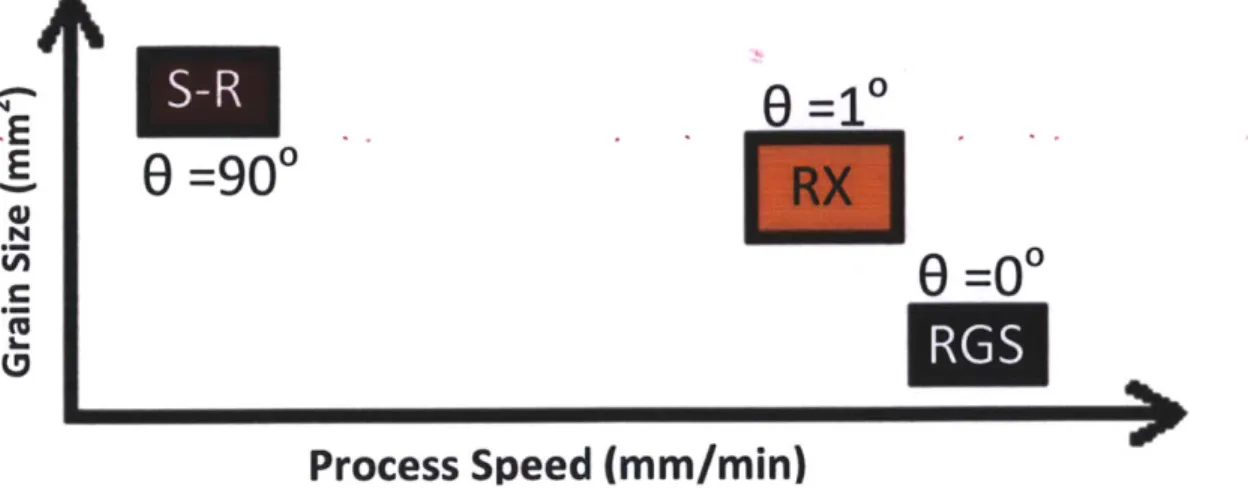
How readily a ribbon process can grow large grains at accelerated process rates is indicated by the angel of its solidification profile, as shown in Figure 20. If the angle is too small, as is the case with RGS, there is no driving force to directionally propagate existing grains and island growth occurs. If the angle is too large, as is the case with String-Ribbon processes, then the process rate is limited by the amount of heat extracted through the interface, as shown in Figure 21.
qy
Figure 20: Schematic of Solidification Interface of RX Wafer
This chapter focuses on identifying the conditions needed to grow existing grains at accelerated process rates. The following section, Heat Extraction through Existing Grains, will first derive a basic heat transfer expression that relates the interfacial velocity (Vyr) to the heat flow (qy) from the surface of the wafer. This theory will be used to design a recrystallization furnace for high process speeds. Section 3.4 will then develop a relationship between the heat flow of the furnace
and the average expected grain size for a wafer. This theory will be used to identify the process rate limitations of the existing RX furnace and potential paths for improvement. Finally, this chapter will end with experimentally reducing the number of preferential nucleation sites on the oxide capsule to reduce nucleation ahead of the growth front.
.ES-E
=900
4)
8=0*
Process Speed (mm/min)
Figure 21: Qualitative diagram of the trade-offs in grain size and process speed for existing silicon ribbon processes
3.3 Heat Extraction through Existing Grains
The relationship between the solidification angle and the rate of heat transferred from the surface of the wafer is critical for the design of the RX furnace. The diagram provided in Figure 20 shows that the interfacial velocity can be geometrically related to the process rate and the angle.
VINT = VH sin 0 (4)
where VINT is the velocity of the interface, VH is the process rate, and 0 is the solidification angle. Furthermore, the rate of solidification can be directly related to the amount of heat removed from the surface by
thhfs = qyx = hs p LVnt (5)
where qy is the incremental heat flow from the surface of the wafer, x is the horizontal length of the solidification profile, hfs is the latent heat of silicon, p is the density of silicon, and L is the length of the solidification interface. Combining Equation 4 and Equation 5 yields the relationship between the solidification angle and the heat flow from the surface of the wafer for a given process rate, as given by
qy = hfsVHp tan 0 (6)
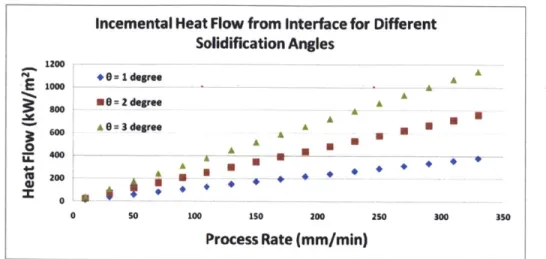
Chalmers claims that a solidification angle of only 1 is necessary to directionally propagate an existing grain.J91 Figure 22 shows that as the speed of the process increases, the amount of heat that must be extracted to maintain a given small solidification angle scales linearly. For accelerated process speeds, the RX furnace will have to be designed to remove a substantial amount of heat from the surface of the wafer. Existing String-Ribbon processes are presently limited to ~40 mm/min, whereas RGS processes have yielded material at over 200 mni/min.
Figure 22: Heat flow required from the wafer to the furnace for a given solidification angle as a function of process rate
3.3.1 RX Furnace Design
Heat extraction from the surface of the wafer must be sufficient to maintain a solidification angle that will not result in island growth. The RX furnace must be designed to remove heat quickly from the wafer as it solidifies, as shown in Figure 23. This section focuses on how the radiation profile of the solidification zone was tailored to rapidly remove heat from surface of the wafer as it crystallizes.
Solidification Zone nuato
loadHeating Elem
I
sulation
Figure 23: Solidworks model and illustration of the solidification zone in the RX furnace A section of the wafer begins to cool down and solidify once the amount of heat it receives from the heating element is less than the heat flow that the wafer radiates to the surrounding insulation. The contributing sources of heat transfer to the wafer at the solidification zone are approximately
4y= 4element + 4insulation = Fea7eeTel - ebpTp) + ( -- e (ebPT*p - EinsT 1,) (7)
where 4eiement
is the heat flow from the element to the wafer, 4insulation is the heat flow from
the insulation to the wafer, Fe is the radiation view factor from the element to the backing plate, Ee is the effective emissivity of the element, Ebp is the effective emissivity of the backing plate,
Eins is the effective emissivity of the insulation, Te is the temperature of the element, Tbp is the temperature of the backing plate, and Tis is the temperature of the insulation. The two alterable
Incemental Heat Flow from Interface for Different Solidification Angles 1200 -00 = 1 degree A A *=2degree A amA A A 0= 3 degree A A 4d A (U 200 X= A 0 01 *U .* 0 50 100 150 200 250 300 350
parameters in Equation 7 are the view factor from the element to the backing plate (Fe) and the emissivity of the insulation (E1ns).
The radiation view factor (Fe) is the element's radiation profile on the horizontal axis of the wafer. The radiation profile from the element to the wafer becomes more concentrated as the distance between the element and the backing plate diminishes, as shown in Figure 24. Concentrating the view factor between the substrate and the heating element reduces the radiation transfer from the element to the wafer as it travels further into the solidification zone. Reducing the amount of heat flow from the elements to the substrate stack in the solidification zone allows the wafer to cool and solidify more quickly. Therefore, to minimize the heat flow from the heating elements to the backing plates in the solidification zone, the spacing between the heating elements and the wafer must be minimized.
002 Z I
0 015
f-0.005 .
Figure 24: View factor from
05 1 15 2
Horizontal Axis (cm)
the element to the backing plate distance from the substrate
as function of the elements
The surface roughness and emissivity of the insulation govern how fast heat is removed from the wafer in the solidification zone. If the surface of the insulation material is rough, it will scatter incident radiation from the backing plate to a cooler region of the furnace. If the insulation material has a low emissivity, then it will reflect the majority of the radiation incident on its surface. Low emissivity insulation therefore has a lower temperature than high emissivity insulation.
An insulation material that has both a low emissivity and a high surface roughness removes will remove heat from the wafer faster than other insulation choices. As shown in the qualitative ray
3 mm between element and substrate
5 mm spacing
7 mm spacing U W.
tracings in Figure 25, this insulation type scatters incident radiation from the wafer away from the solidification zone to regions of the furnace with a lower temperature.
HIaTi
acin
Pls
U
S.
Figure 25: Ray tracing illustration of the radiation profile at the solidification zone. The low emissivity insulation reflects incident radiation at the same wavelength. High emissivity
insulation emits the radiation spectrum of its temperature profile. High surface roughness results scatters heat from the backing plate to cooler regions of the furnace.
A zone-melting furnace was constructed to remove heat quickly from the wafer at the solidification zone. The hot zone consisted of four sets of closely spaced silicon carbide (SuperSiC©) heating elements that exhibited working temperatures up to 16900 C in ambient atmosphere. The low emissivity, high surface roughness insulation material used was mullite, and the interior of the furnace is lined with a rectangular quartz tube to limit contamination. The temperatures of the elements are monitored by three independent dual colored pyrometers that are positioned over the elements. These pyrometers feed directly into a LabView program which controls three phase-angle fired SCRs. Typical operating conditions for running samples at 100 mm/min require the elements to be at ~1680* C, which requires each set of two elements provide
~200 W at 240 V.
3.3.2 RX Furnace Characterization
As described by Equation 6, the heat flow from the substrate stack in the solidification zone dictates the solidification profile of the wafer. This section determines the magnitude of heat flow from substrate stack in the RX furnace.
To measure the amount of heat leaving the stack as the wafer solidifies (4 ), a thermocouple was sandwiched between two silicon carbide backing plates and shuttled through the furnace. For different process rates, the measured temperature profile of the RX furnace is plotted as a function of position in Figure 26.
Measured Zone Melting Furnace Temperature Profile
1450 W10mm/mm 1640 C A20 mm/m n 1640 C A20mm/mn1640C 30 mm/min 1640 C 140mm/mn1640C 1350 *40mm/min 1660C Last Element; 1250 ' ---1200 A 100 110 120 130 140 150 160 170 180 190 200 Poshion in Furnace (mm)
Figure 26: Thermocouple measurements of the zone-melting furnace rates and temperature set points
at different process
Because silicon carbide does not undergo any phase transformation at the melting temperature of silicon, its temperature simply depends on the amount of heat leaving the substrate. The rate at which the silicon carbide stack cools is
4y = PsiccsictsicT (8)
where Psic is the density of the SiC substrates, tsic is the thickness of one silicon carbide substrate, csicis the specific heat of the SiC substrates, T is the rate of temperature change of a region of the backing plate.
The combination of Equation 8 and Equation 7 can predict the amount of heat flow from the silicon carbide substrate stack as it enters the solidification zone. Assuming that the temperature of the insulation is 12800 C and that the elements are 3 mm from each side of the substrate stack, Figure 27 shows the expected respective heat contributions from the element and the insulation as a function of the backing plate's position in the solidification zone.
Figure 27: Model of Heat Flow to Backing Plate as a Function of Position
Given the expected heat flow profile in Figure 27, the expected temperature of the silicon carbide substrate can be found by incrementally by
Ti+1 = Ti + X) * VH
psiccsictsic x (9)
where Ti is the old temperature of the backing plate, Ti+1 is the new temperature of the backing plate, and 4y (Ti+1, x) is the heat flow from the wafer as a function of position and the
temperature of the backing plate. Equation 9 and Equation 7 can be used jointly to model the temperature profile of the silicon carbide backing plate as it enters the solidification zone. Figure 28 plots the model's predicted temperature profile of the backing plate alongside the measured thermocouple data for a process rate of 40 mm/min.
Figure 28:
Measured Temperature Profile of RX Furnace and Simulation
1450 + Meas' 1400 -- - -- - -- - -0 Mode S1350 Center of E 1300 IV Last Element 1250 1200 155 165 175 185 195 Position In Furnace (mm) ured 205
Predicted and Measured Temperature of the Backing Plate as it Enters the Solidification Zone
Heat Flow to Section of the Backing Plate with Thermocouple and No Silicon Wafer
200 Z00[ -N Heat from Element
A Heat to Insulation *Net Heat E 100 50 A A 0 0 0 910 15 20 -*.. -100
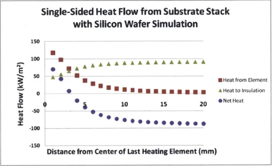
Since the simulated temperature profile matches well with the measured data, the model seems to accurately simulate the radiation profile of the furnace. Therefore, this radiation model can now be tailored to simulate the heat flow from a substrate stack with the silicon wafer. The heat flow from the. silicon carbide substrate stack that contains. the silicon wafer will, differ from the thermocouple measurement because the substrate stack will remain at the melting temperature of silicon as the wafer solidifies. Therefore, the heat flow from the stack with the wafer will be respectively greater because the temperature difference between the substrate stack and the furnace will not decrease as the latent heat from the wafer is removed. Figure 29 simulates the heat flow from the substrate stack with the wafer as it enters the solidification zone of the RX furnace. Figure 29 assumes that wafer emits radiation through only one side.
Single-Sided Heat Flow from Substrate Stack
with Silicon Wafer Simulation
150 --- 15
100
-50 +n -50om ~ C of Ltei Element
F 2A Heat to Insulation
0 10 5 20 Net Heat
-100
Distance from Center of Last Heating Element (mm)
Figure 29: Simulated heat flow from substrate stack with silicon wafer. Single-sided heat removal assumed.
Given the simulated heat flow from the substrate stack, the solidification profile of the wafer can be found by
t+1 = ti + 4y(Psthfs 4 1 4, X) * x (10)
where ti is the incremental thickness of the solidified wafer. Figure 30 shows the simulated solidification profile of the wafer in the RX furnace.
Figure 30: Simulated Solidification Profile of Wafer in RX. assumed.
Single-sided heat removal
If it is assumed that the solidification profile in Figure 30 is linear, then the solidification angle of the wafer can be simply found by
6soltdification = tan- twafer
Lso1ldify (11)
where Lsoidiry is the length of the solidification profile and twafer is the thickness of the wafer. Figure 31 shows the simulated solidification angle as a function of the process rate for the RX furnace. The desired 10 solidification angle occurs at process rate of approximately 60 mm/min. Furthermore, the solidification angle can be used with Equation 4 to find the interfacial velocity of the wafer at a given process rate, as shown in Figure 31.
Modeled Solidification Angle and Interface
Velocity as a Function of Process Rate
1.4 1.2 1.2 E 1 E 0.8 E - 0.6 -O.9 S0.4 0 " 0.2 0.8 0 0.7 20 40 60 80 100 120 140 m
Process Rate (mm/min) C
Figure 31: Simulated Solidification Angle and Interfacial Velocity of Wafer.
Model of Single-Sided Solidification Profile in RX Furnace
200 - - - -180 T_160 2 140 120 --- 40mm/n - -60 mm/ n 60 80 mm/ 40 20 -+-120 mm/ 0 0 5 10 15 20 minute minute minute /minute /minute 25
In summary, this section develops a radiation model of the RX furnace that predicts the temperature profile of a silicon carbide substrate stack that was shuttled through the RX furnace. This radiation model was used to characterize the incremental heat loss from the substrate stack as the wafer solidifies in the RX furnac.e.. This heat flow was related to the solidification. angle of the wafer at different process rates in the RX furnace. Given the solidification profile of the wafer, the following sections will focus on limiting nucleation ahead of the growth interface.
3.4 Nucleation Suppression Ahead of Solidification Interface
Because the rate of solidification and the rate of nucleation are both dependent on the level of undercooling sustained in the melt, the probability of heterogeneous nucleation occurring on the surface of the capsule increases as the driving force of solidification increases. This section focuses on minimizing the nucleation rate ahead of the solidification interface.
This section will first relate the interfacial velocity of the wafer to the amount of undercooling sustained in the melt in front of the interface. Next, this undercooling will be related to the nucleation rate ahead of the interface. For a given process rate, capsule material, and heat flow from the wafer to the RX furnace, the nucleation rate will then be used to predict the relative number of grains on the wafer per unit area. This section will then identify and reduce the number of preferential nucleation sites so as to further reduce the number of grains on the wafer per unit area.
3.4.1 Relationship between Interfacial Velocity and Melt Undercooling
This section will develop a conceptual understanding of how the interfacial velocity of the wafer is related to the undercooling of the melt ahead of the solidification interface. The driving force of crystallization is proportional to the undercooling at the solidification interface and is given by:
_F hfSAT
VmTm (12)
Where hf, is the latent heat of fusion in J/mol, AT is the undercooling, Tm is the melting temperature, and Vm is the molecular volume of the solid. Based on the driving force of solidification, an interface can advance by either discontinuous, screw dislocation growth or by continuous growth. Discontinuous growth occurs at low undercoolings where the interface advances via discrete steps. Continuous growth occurs when the critical radius of nucleation is comparable to the size of the advancing steps. This rapid growth mechanism is characterized by grain refinement and cellular growth and is not preferred. The critical driving force that distinguishes the boundary between the two growth mechanisms is
-aAF* = irg (13)
where a is the lateral spacing of growth, - is the interfacial energy between solid and liquid silicon, and g is the ordering parameter. The critical undercooling for silicon above which continuous growth would occur is
AT* = goVMTm
ahfs (14)
The lateral spacing of growth is approximately the distance between neighboring silicon atoms in the crystal lattice. Furthermore, Jackson et al claim that high entropy -of fusion materials, like silicon, have sharp interfaces. 01 Hillig and Turnbull assert that for sharp interfaces, g~1.1"I For the parameters given in the Table 2, the critical undercooling for silicon is calculated to be 2230 K. Parameter Value g 1 a .438 J/m21 1 Vm 3.34 X 10⁻⁶ m3/mol hfa 50.2 kJ/mol a 2.2 X 10 0 m Tm 1683 K D 4 X 10~ m2/s [13
Table 2: Parameters used to determine the growth mechanism for silicon
This calculation is consistent with undercooling studies performed by Li et al, as shown in Figure 32.112] Because experiments performed by Appapallia show that encapsulated silicon wafers typically nucleate well below this level of undercoolin , the solidification interface is likely to advance in the RX process by screw dislocation growth.
(b) 2mm (c) 30pgm
Fig. 4.- SEM surface relief (unetched) of pre Si grown at diferest undercoolings, a) AT = 57 K and c) AT = 420 K. Optical microstructure externally triggered at b) AT = 220 K.
Figure 32: Undercooling studies reveal that silicon does not exhibit the grain refinement typical to continuous growth until the melt is undercooled beyond 2200 K 1121
Hillig and Turbull relate the velocity of screw dislocation growth in high entropy material to the undercooling of the interfacial melt by
W 3DhfSAT
aRT2 (15)
where D is the self-diffusion coefficient of liquid silicon given in Table 2."13 The screw dislocation velocity is related to the interfacial velocity by
(16) Vnt = 41rrcvo0a
where rc is the critical radius of nucleation on the interface, given by a
rc = A- F
The relation between the melt undercooling and the interfacial velocity is
- 3Dfs,2 T
2
RT2(47F)GTmVm
(17)
(18) How the interface growth rate relates to the undercooling of the silicon melt is shown in Figure
33. This figure shows that only a small level of undercooling is needed to quickly propagate the interface. This will be important when discussing preferential nucleation sites in the next section.
Figure 33: Interface Growth Rate as a function of the undercooling of silicon
This section has related the level of undercooling in the silicon melt to the growth rate of the solidification interface. The next section will now relate the level of undercooling in the melt to the nucleation rate ahead of the interface.
3.4.2 Relationship between Melt Undercooling and Nucleation Rate
The probability of a nucleation of a new grain occurring ahead or on the surface of the solidification interface is dependent on the level of undercooling exhibited by the melt. The expression for a heterogeneous nucleation rate on the capsule wall is
-AGhet
J = Joe kr SA (19)
where Jo is a constant that scales linearly with the number of nucleation sites for heterogeneous nucleation available per unit area, k is the Boltzmann constant, AGiet is the heterogeneous nucleation driving force for the critical radius of nucleation, SA is the surface area of the interface on which nucleation occurs, and T is the temperature at which nucleation occurs. AGiet is the free energy of the critical radius of nucleation given by the expression
Interface Growth Rate and Process Rate for
Solidification Angle
9
= 10 as a Function of
Undercooling
E 600 E 500 E 400 a, 300 i - 200 100 t 0 %A 0.2 0.3 0.4 0.5 0.6 0.7 4 Undercooling (K) lk MAGhet = AGvVs iucon + Ailsa1is =
f
Vsiicon + Aitso1 is) (20)where AGnuc is the energy of reduction achieved by the nucleation of a particle, AG, is the is the volumetric -free energy difference between the solid and liquid phases, Vsjicon is -the volume of solidifying silicon, Aits is the interfacial area between the solid and liquid/substrate interface respectively,
cits
is the interfacial energy of the solid and the melt/substrate, hfr is the latent heat of fusion, AT is the amount of undercooling experienced by the melt, and Tm is the melting temperature. The critical radius of nucleation is associated with the apex of the free energy curve and can therefore be found by differentiating Equation 12 and setting it equal to zeroa_____= 0
(21)
r* - 2_zmTm (22)
Gy hfsAT
AGiet = f (16 (23)
where AT is the level of undercooling that can be sustained by the given capsule material, hfs is the latent heat of silicon, Tm is the melting temperature of silicon, f is the heterogeneous compensation factor specific to the capsule material given by
f = cos si + 1(cos s (24)
where Osi is the contact angle between the silicon and the capsule material. In a levitation suspension setup, Li et al. measured the interfacial energy between liquid and solid silicon to be .438 J/m2.['2 1 Quartz and liquid silicon have been documented to have a wetting angle
of~-85",1131 and SiN has been documented to have a wetting angle of-420 with liquid silicon. [41
Figure 34 relates the relative nucleation rate of a given capsule material to the level of undercooling in the melt. The nucleation rates for each respective capsule material are normalized to a given number of nucleation sites so that the material properties can be respectively compared. A 'rough' surface is modeled to have three times the surface area of a 'smooth' surface, and therefore three times the nucleation rate.
0.7 i 0.6 o 0.5 -o 0.4 Z - 0.3 R 0.2 00.1 Z
Nucleation Rate for Different Materials
Related to the Undercooling of the Melt
SHomogenous AL OSmooth QuartzAA X Rough QuartzA A A s R Qu a r t z U -0 W = - W O - VV V 0.1 0.15 0.2 0.25 0.3 0.35 0.4 0.45 0.5 Undercooling (0K)
Figure 34: Normalized nucleation rate for different capsule materials as a function of undercooling
Figure 34 shows that a SiN capsule would consistently have a significantly higher nucleation rate than a quartz capsule. Furthermore, the difference between SiN and quartz capsule's respective nucleation rate grows with the level of undercooling of the silicon melt. Alternatively said, a SiN capsule that experiences a low level of undercooling would have comparable nucleation behavior to a quartz capsule at a high level of undercooling.
3.4.3 Grain Size in Wafer Related to Process Rate and Heat Extraction from the Solidification Interface
Up to this point, the following relationships have been forged. The heat flow from the substrate stack to the RX furnace and the process rate has been related to the interfacial velocity by Equation 5. The interfacial velocity of the wafer has been related to the undercooling of the melt
by Equation 18, and the undercooling of the melt has been related to a material's nucleation rate by Equation 19. Using these relationships, the number of grains that occur per unit area of the wafer can be found by dividing the rate of nucleation (particles/time) by the respective process rate (Area/time). For a given amount of heat flow from the wafer to the furnace in the solidification zone, the average number of grains in a wafer is
N = 1
(25)
A VH
where J is the normalized rate of nucleation, N/A is the relative number of nucleation for a given surface area. Equation 25 can be used to determine the process rate for a given RX furnace to
minimize the number of grains in a recrystallized wafer. As shown in Figure 35, an RX furnace should be designed to maintain a shallow solidification angle for a desired process rate to have the fewest total number of grains per unit area. This result is intuitive because a smaller solidification angle will result in a lower interfacial velocity for a given process rate. And a
lower interfacial velocity requires less undercooling of the melt, which results in a lower nucleation rate.
Normalized Nucleations per Area for Different Solidification Angles with Smooth Capsules
-+-0=1,Quartz -0-0=2,Quartz -*-0=3,Quartz -- =.5,SiN
05
0
* 1.5
0.5
Z 0 100 200 300 400 500 600
Process Rate (mm/min)
Figure 35: Normalized number of nucleations per unit area for different solidification angles for different capsule materials
Figure 35 shows that the number of grains per area initially has a proportional relationship with the process rate, but then declines after a critical point. This suggests that the process rate of the RX concept is limited by the amount of heat that can be extracted from the interface. Therefore, future RX furnaces can be designed using Figure 35 in combination with Figure 22.
The normalized number of grains per unit area of a wafer with a given capsule material is shown in Figure 35. The relative number of grains per unit area decreases significantly for the SiN capsule as the process rate rises.
However, for the existing RX furnace, the present theory can predict the number of grains per unit area for a given process rate and sample preparation. Figure 36 shows that for a process rate of 60 mm/min, a wafer recrystallized with a SiN capsule should exhibit ~1OX the number of grains exhibited by a wafer recrystallized with a thermally grown oxide capsule.
Normalized Number of Grains per Area for a Given
Process Rate for the Heat Flow from the RX Furnace
4.5 + Smooth Quartz 5 1 - -- -_--3 -f --- - - - -2.5 A Rough Quartz 2 -U --- ---0 ---.- -.... -1 -- ---- W 0.5 *0 Z 2S 35 45 55 65 75 a5 95 105 115 125
Process Rate (mm/min)
Figure 36: Normalized number of grains formed per unit area of wafer for a given process rate for the measured heat flow from the RX furnace
The two wafers in Figure 37 qualitatively demonstrate this relationship.
SIN Capsule
Thernally Grown Oxide Capsule
Figure 37: SiN and Oxide encapsulated wafers recrystallized at 60 mm/min in the RX furnace
This section has developed a conceptual understanding of how the number of grains in a wafer relates to the capsule material, process rate, and radiation profile of the RX ftirnace. However, the nucleation rates found in this section scale with the number of preferential nucleation sites on the capsule, as described by Equation 19. Therefore, the next section will focus on the identifying and reducing the number of preferential nucleation sites on the oxide capsule (Jo) and the amount of surface area on which nucleation can occur (SA). The following sections will develop a conceptual understanding how these two parameters can be tailored to suppress heterogeneous nucleation.
3.4.4 Experimentally Observed Relationship between the Preferential Nucleation Sites on a Thin Oxide Capsule and the Nucleation Rate (Jo)
The heterogeneous nucleation rate on the capsule surface scales with the number of preferential nucleation sites per unit area. This section identifies the type of defect that typically triggers nucleation and experimentally develops methods to reduce this defect's occurrence.
For a given material, a preferential nucleation sit6 is a defect that locally lowers the energy barrier to nucleation. A structural defect on the capsule can be a preferential nucleation site if its size is comparable to that of a nucleating particle. If a defect on the capsule is smaller than this dimension, it will congregate too few atoms to overcome the interfacial energy of a new phase and will therefore not trigger a nucleation. Defects that are significantly larger than this dimension will energetically resemble a flat surface and will therefore not preferentially trigger a nucleation. Varanasi claims that the size of a structural defect must be between one and fifty times the critical radius of nucleation for it to be a preferential nucleation site.
The critical radius, or minimum size of a stable nucleating particle, can be found by setting the differential of the free energy curve for nucleation to zero, as described by Equation 22. For a given solidification angle, the relationship between the critical radius of nucleation and the process feed rate is given in Figure 38. As shown, a structural feature that is between -200 nm and 10 pm can therefore act as a preferential nucleation site for process rates of -60 mm/min. Reducing the number of structures that are comparable in size to the critical radius of nucleation will reduce the overall nucleation rate.
Critical Radius of Nucleation for a Given
Process Speed,
= 10
500gE
c: 400 300 M200 M 100 10 60 110 160Process Speed (mm/min)
Figure 38: Critical radius of a nucleating silicon grain for a given solidification angle Two types of structural features are typical on the capsule of the wafer. The first one occurs when the wafer melts and locally pulls the oxide capsule inward, as shown in Figure 39. However, the size of this deformation is typically on the order of 10s of microns and generally very smooth, making this site less likely to act as a preferential nucleation site.
Figure 39: Partially melted silicon RX wafer with texture etching. The encircled 'speckles' are small melt pools that thin down and deform the capsule locally.
The quartz powder release layer is a more likely source for preferential nucleation sites. Structures that are on the order of 10 micron can be created by the multiple point contacts made between quartz powder release layer and the capsule. Furthermore, an irregular layer of quartz powder can increase the amount of interfacial area between the melt and the oxide capsule, making nucleation more likely.
A set of experiments were conducted to isolate the mechanism by which the quartz powder release layer influences the nucleation rate. The first experiment involved recrystallizing two samples with and without a thermally grown oxide capsule. Both samples were confined by a quartz powder release layer of the same thickness. As shown in Figure 40, the wafer without an oxide capsule conformed more readily to the geometry of the quartz powder release layer, resulting in more interfacial area between the melt and quartz. The wafer encapsulated in a thin oxide, on the other hand, did not conform as readily to the release layer, but instead made small point contacts with the powder.
r O Thin oxide film casule