HAL Id: hal-01413097
https://hal.laas.fr/hal-01413097
Submitted on 9 Dec 2016HAL is a multi-disciplinary open access archive for the deposit and dissemination of sci-entific research documents, whether they are pub-lished or not. The documents may come from teaching and research institutions in France or abroad, or from public or private research centers.
L’archive ouverte pluridisciplinaire HAL, est destinée au dépôt et à la diffusion de documents scientifiques de niveau recherche, publiés ou non, émanant des établissements d’enseignement et de recherche français ou étrangers, des laboratoires publics ou privés.
High Spatial Resolution Imaging of Transient Thermal
Events Using Materials with Thermal Memory
Olena Kraieva, Carlos M. Quintero, Iurii Suleimanov, Edna Hernandez, Denis
Lagrange, Lionel Salmon, William Nicolazzi, Gábor Molnár, Christian
Bergaud, Azzedine Bousseksou
To cite this version:
Olena Kraieva, Carlos M. Quintero, Iurii Suleimanov, Edna Hernandez, Denis Lagrange, et al.. High Spatial Resolution Imaging of Transient Thermal Events Using Materials with Thermal Memory. Small, Wiley-VCH Verlag, 2016, 12 (46), pp.6325-6331. �10.1002/smll.201601766�. �hal-01413097�
High spatial resolution imaging of transient thermal events
using materials with thermal memory
Olena Kraieva1,2, Carlos M. Quintero2, Iurii Suleimanov1,3, Edna M. Hernandez1,4, Denis Lagrange2, Lionel Salmon1, William Nicolazzi1, Gábor Molnár1,*, Christian Bergaud2,* and Azzedine Bousseksou1,*
*Corresponding authors. E-mail: [email protected], [email protected],
1LCC, CNRS & Université de Toulouse, UPS, INP, F-31077 Toulouse, France. 2LAAS, CNRS & Université de Toulouse, INSA, UPS, F-31077 Toulouse, France. 3Department of Chemistry, Taras Shevchenko National University of Kyiv, Kyiv, Ukraine. 4Facultad de Ciencias, Universidad Nacional Autónoma de México, Mexico City, Mexico
The accurate control of temperature is a common requirement in science and technology. In particular, although much effort has been devoted in the past decade to the development of nanoscale thermometry methods, we currently lack the tools to map transient thermal events with high spatial resolution. Here we experimentally demonstrate the working principle of a new kind of nanothermometer using materials with thermal memory as time-temperature integrators. As an application, we tackle the outstanding problem of spatially resolving a brusque erratic heating event in an operating microelectronic device. We show that a spatially and temporally confined temperature change leads to a local (reversible) modulation of the optical properties of our material. Thanks to the virtually infinite lifetime of the metastable states within the bistability region, this optical information can be retrieved later on by a simple reflectivity measurement, either in far- or near-field. This concept enabled us to acquire sub-wavelength resolution images of transient (s scale) heating events.
The recent tendency of miniaturization and achievements in nanoscience and nanotechnology brought about the necessity of accurate temperature measurements on a reduced size scale [ 1-4]. In addition, the heat exchange in tiny volumes occurs promptly, hence the measurement needs to be done most often in a limited time window. The lack of spatio-temporal resolution and the increasingly invasive nature of common temperature sensors are the main obstacles
one has to overcome in order to achieve this aim. Nanothermometry needs, therefore, a novel paradigm both in the use of materials and thermometric properties. When spatial resolution is important, the most promising techniques are those involving scanning probe microscopies (SPM). For instance, scanning thermal microscopy (SThM) uses thermocouple or resistive probes to map the temperature and/or thermal properties of the surface [5]. These methods can nowadays achieve a spatial resolution of a few tenths of nm [6]. However, as they use contact probes and point-by-point data acquisition they are often invasive and their imaging speed is very slow (typically a few seconds or even minutes). Similar issues arise with electron microscopy-based thermometry techniques, which were reported to reach even sub-10-nm spatial resolution [7]. On the other hand, for high temporal resolution nanothermometry, the most popular techniques are based on far-field optical imaging, such as fluorescence [8] or reflectometry [9]. For example, sub-nanosecond resolution thermal images can be obtained using thermoreflectance. In these cases, however, the spatial resolution is restricted by the diffraction limit.
Here, we present the first experimental realization of a nanothermometry approach, which combines the high spatial resolution of SPM methods with fast transient imaging capability. Our approach uses a thermosensitive film whose optical properties are temperature dependent. From this aspect our method bears a resemblance to the well-established liquid crystal thermometers [10]. The primary difference is that in our case the optical properties exhibit a wide thermal hysteresis and the thermometer is used within this bistability region. As a consequence of this thermal memory, the thermally-induced optical changes can be read out even long after the dissipation of heat. In other words the temperature changes can be mapped
ex-situ, which is the key interest here, since it allows for using slow imaging methods, such as
SPMs, to map fast, transient thermal events.
There are many different materials which exhibit phase transitions with large thermal hysteresis, such as metallic alloys (e.g. NiTi), chalcogenide glasses (e.g. GeSbTe), transition metal oxides (e.g. VO2) and certain transition metal complexes displaying spin transition, valence tautomerism or other cooperative electronic switching phenomena, just to cite a few. The material choice for the targeted application is reduced, however, by rather stringent experimental constraints. These include the need for a wide (several tenths of Kelvin) and abrupt hysteresis centered at a technologically relevant temperature range, fast phase change kinetics (s), the possibility to process the material as a high quality, large-area,
sub-micrometer thin film without altering its properties, a detectable change of physical properties and resistance to fatigue upon successive thermal cycling. Depending on the applications additional requirements may arise. For example, in the case of microelectronic applications the material must be insulating. To demonstrate the feasibility of our concept we used bistable thin films of the spin crossover (SCO) complex (1) [FeII(Htrz)
2(trz)]BF4 (Htrz = 1,2,4-triazole and trz = 1,2,4-triazolato).
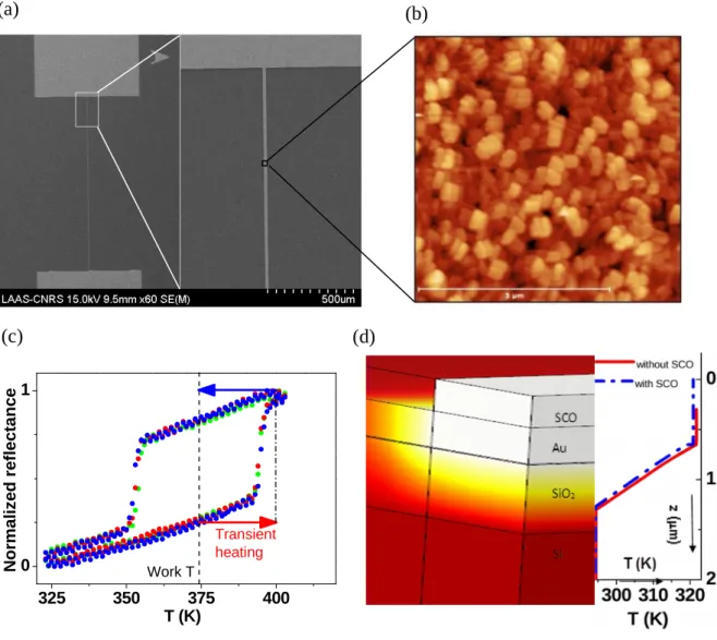
Rod shaped nanoparticles of 1 with a mean size of ca. 150 nm (length) x 80 nm (width) were dispersed in ethanol and spin coated on the surface of microelectronic test devices. These latter consist of rectangular gold microwires (length 1 mm, thickness 350 nm) with different widths (2 - 8 m), which were fabricated on an oxidized Si wafer by conventional photolithography and lift-off techniques. Due to their small thermal mass, the temporal response of the wires is fast and the heating is spatially well confined. These assets, together with their reliable all-electrical operation (i.e. resistive heating and temperature reading) make these wires ideal test benches for the development of nanothermometry materials - both in static and dynamic regimes [11]. Fig. 1 shows scanning electron microscopy (SEM) images of a microwire device as well as the atomic force microscopy (AFM) topography of the spin-coated nanoparticle film of 1 (see also Fig. S1-S2). A dense coverage was obtained over the whole surface of the device with an average thickness of ca. 300 ± 50 nm. The bistability range of the thermometer film was determined by far-field optical reflectivity measurements. As depicted in Fig. 1c, upon heating the reflected light intensity increases nearly linearly up to 393 K where it exhibits an abrupt increase of ~3 %. In the cooling mode opposite changes are observed with an abrupt drop of the reflectance around 353 K defining a perfectly reproducible, ca. 40 K wide thermal hysteresis loop. The abrupt reflectance changes correspond to the well-known spin transition of 1 between the low spin (LS) and high spin (HS) electronic configurations [12]. Far from the spin transition, the increase of reflectance with temperature can be accounted for ordinary thermal expansion and associated refractive index changes. On the other hand, the brusque change of the reflectance upon the spin transition is primarily related to the very significant strain (V/V = 11 % [13]) and concomitant refractive index variation, which accompanies the phase transition in 1. Obviously, the measured reflectance depends not only on the spin crossover layer, but also on the composition and thickness of the device materials as well as the wavelength, propagation direction and polarization state of the probe light and must be thus calibrated in each case.
325 350 375 400 0 1 N o rm a liz ed r ef le ct a n ce T (K) Transient heating Work T
Fig. 1. Microheater device with a thermosensitive SCO coating. (a) SEM images of a gold
microwire heater. (b) AFM topography scan of the SCO film spin-coated on the surface of the heater. (c) Variable temperature optical reflectivity signal of the microwire device covered by a 300 nm thick SCO layer acquired for three consecutive thermal cycles between 323 and 403 K. The red arrow represents in a schematized way the transient thermal information, which is stored in the memory of the material when the wire is excited by a current bias. (d) Steady-state 3D temperature distribution in the microwire under 50 mA current bias simulated using COMSOL and the corresponding depth (z-axis) temperature profile of the device both in the presence and absence of the SCO layer.
Thermometry methods based on a surface coating are usually classified as semi-invasive as they introduce inevitably some disturbance to the temperature field [14]. To investigate the impact of the film of 1 on the temperature distribution in our device we have carried out a detailed numerical simulation both for steady-state and transient heating. We solved the heat conduction equation by finite element analysis using the COMSOL program. The average temperature of the wires was also determined experimentally from steady-state and time-resolved electrical resistance measurements (see Fig. S3-S4). As an example, for a sharp,
step-(b) (a)
like current excitation of 50 mA, the simulated/measured temperature jumps are 27 K/23 K and the corresponding thermal rise times are 1.01 s/0.98 s. The agreement between experiments and simulations is satisfactory, considering that the latter were carried out without any free parameter adjustment. Fig. 1d depicts a steady-state simulation result for a microwire covered by a 300 nm thick layer of 1. From a first qualitative inspection it is clear that the heating is strongly confined to the wire and the material on top of it. Basically the temperature distribution is uniform within the gold wire and the SCO compound covering it, while ca. 1 m away from the wire its environment is at ambient temperature in all spatial directions. In a more quantitative manner, Fig. 1d shows also the temperature depth profile in the z direction, i.e. normal to the surface, both in the presence and in the absence of the thermometer layer. One can observe less than 0.1 K difference between the bottom of the gold wire and the top of the thermometer layer. This means that our thermometer measures very precisely the surface temperature of the device. Concerning the invasiveness of the thermometer material, the performance is also very good since the temperature of the gold wire in the absence and presence of the thermometer differs by less than 1 K. (Obviously, if the device is scaled down the thickness of the thermometer layer must be also reduced to keep this performance.)
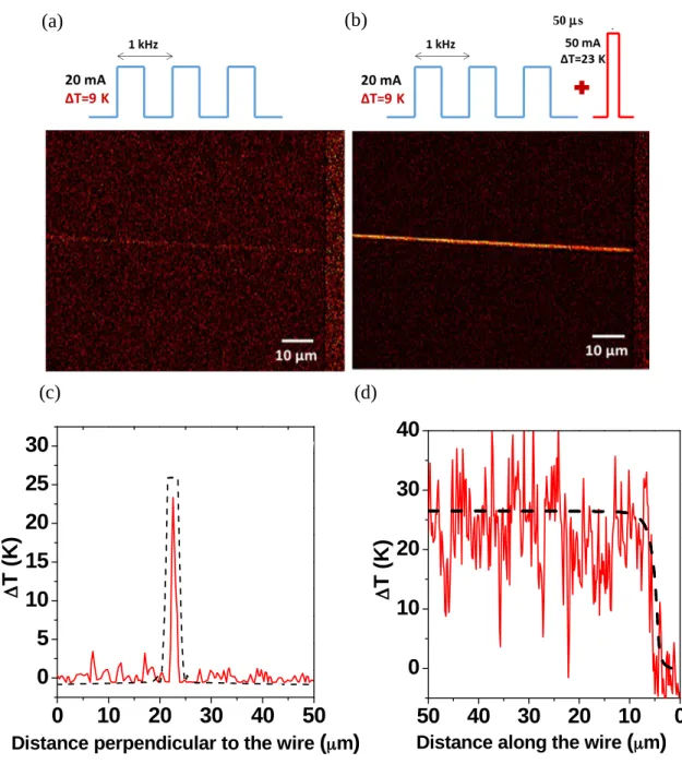
A possible application of our nanothermometer is the spatially resolved detection of overheating above a threshold temperature in different parts of a micro/nanoelectronic device during its long-term operation. Indeed high density integrated circuit packing and increased switching speeds can lead not only to increased average chip temperature, but also to local hot spots, which can significantly decrease the performance and reliability of microelectronic circuits. To demonstrate this application potential of our thermometer, we have reproduced an overheating situation in a microelectronic circuit. We applied to a wire a square ac current with a frequency of 1 kHz and amplitude of 20 mA (Fig. 2a). In these conditions the temperature of the wire rises and decreases alternately by ca. 9 K. This thermal excitation will be considered as the ‘normal operation’ of the device. We thus fixed the temperature of the whole chip at 374 K (see dashed line in Fig. 1c) so as to avoid any spin-state switching in these ‘normal operating conditions’. We let the circuit operate during 30 min under these conditions and have recorded its far-field optical reflectance image by a conventional optical microscope before and after operation. As shown in Fig. 2a the difference of the two images recorded before and after device operation remains rather featureless and it is difficult to conclude about any excess heating. (N.B. It is possible to discern in this image the gold
surfaces with respect to the SiO2, but this difference does not correlate at all with temperature differences, it reflects simply a different measurement noise on different surfaces.) In the next step we repeated the same experiment, but we added a spurious thermal burst of 5 µs duration and 50 mA amplitude over the ac signal during the device operation (Fig. 2b). From electrical resistance measurements we determined that this current spike induces a ΔT of ca. 23 K in the wire, which is high enough to change the spin state of our thermometer from LS to HS (see arrows in Fig. 1c). It should therefore result in a local persistent increase of the optical reflectance. Fig. 2b shows the difference of the reflectance images recorded before and after the ‘faulty operating conditions’ wherein one may note a bright stripe along the microwire. This strong spatial confinement of the reflectance change - associated with the transient heating event - is in excellent agreement with the numerical simulation results, providing thus a clear proof of our transient thermal imaging concept. These reflectance changes were perfectly reversible and reproducible over several switching experiments.
The basic function of our thermometer material is to detect whether or not heating/cooling above/below a threshold temperature has occurred at a given location during a fixed period. Nevertheless in the case of repeatable thermal events it can allow also for the quantification of the temperature changes. Obviously one can only analyze temperature changes smaller than the hysteresis width. On the other hand the temperature resolution is fixed chiefly by the reproducibility of the transition and the signal-to-noise ratio. In the case of 1, at best, one can expect to measure temperature changes as high as T = 35 K with a precision of ca. 1 K. (Of course, higher temperature changes can be still detected, but cannot be quantified.) The temperature measurement is simply based on the comparison of the optical reflectivity signal of the device in the ON and OFF states along the whole temperature range of the hysteresis (see Fig. S5 for details). Using this procedure maps of the transient temperature changes can be constructed as shown for example in fig. 2c-2d. From these maps a well confined transient heating of ca. 23 ± 5 K can be inferred on the microwires - in excellent agreement with the electrical resistance based temperature measurements on the neat wires. Incidentally, this result proves also that the energetic balance is not significantly impacted by the presence of the SCO layer even at this short time scale. Nevertheless, it is important to note the relatively high specific heat of 1 (~1 Jg-1K-1) and the large amount of latent heat associated with the spin transition (~10 Jg-1) may alter the heat distribution in the device, which should be always verified experimentally and/or by numerical simulations.
0 10 20 30 40 50 0 5 10 15 20 25 30 T ( K )
Distance perpendicular to the wire (m)
50 40 30 20 10 0 0 10 20 30 40 T ( K )
Distance along the wire (m)
Fig. 2. Mapping a transient heating event in an operating microelectronic device. (a) Difference
of the optical reflectivity images recorded at 374 K before and after 30 min ‘normal operation’ of the device coated with a layer of 1. The schematic presentation of the ac current applied to the device is also shown. (b) The same image as in (a), but in this case a single current spike (50 µs, 50 mA) was added over the ac current to mimic an erratic heating event in the device. (c-d) Maps of the transient temperature changes perpendicular and along the wire. The simulated thermal profiles are also shown by dashed lines.
The far-field image (ca. 2 m resolution) of a random transient thermal event shown in Fig. 2b would be extremely difficult to acquire by any other thermometry method. Thanks to our bistable thermometer material we could obtain this image in a straightforward way by an ordinary CCD camera under low-intensity light exposure through a cheap ×5 magnification
50 s
(b) (a)
(d) (c)
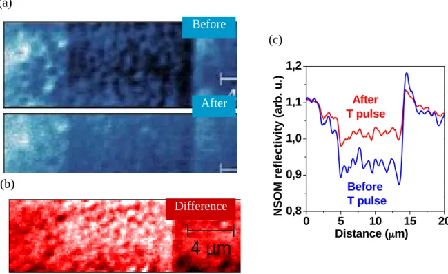
objective. This is a considerable advantage over fast transient thermal imaging approaches. These latter are based on either real-time monitoring or pump-probe techniques and are barely compatible with high resolution SPM imaging. The remarkable advantage with our thermometry approach is that the transient heating information is stored in the memory of our thermometer and can be thus read out using even very slow imaging techniques. An additional advantage is that the SPM probe becomes less invasive since (moderate) temperature changes induced by the SPM probe do not alter the spin-state of the thermometer (Fig. S6). To highlight the outstanding spatial resolution of our nanothermometer we have acquired near-field reflectivity images of our microwire device using near-near-field scanning optical microscopy (NSOM). NSOM images of a device held at 382 K are shown in Fig. 3a before and after applying a current pulse (T = 52 K) to the wire (see Fig. S7-S8 for further images). The difference of the two images (Fig. 3b) allows to discern fine, sub-wavelength details in the heated area. Similar to the far-field experiments a well-localized increase of the reflectance signal is observed on the wire following the current pulse. This is particularly clear in the NSOM cross-sections traced perpendicular to the wire (Fig. 3c).
Fig. 3. Spatial detection limit. (a) NSOM reflectivity ( = 488 nm) images of a microwire covered by a layer of 1. The two images were acquired at 382 K before and after applying a 190 mA current pulse through the wire. b) Difference between the two images shown in (a). c) Averaged and flattened cross-sections of the two images in (a) perpendicular to the wire.
0 5 10 15 20 0,8 0,9 1,0 1,1 1,2 After T pulse N S O M r ef le ct iv it y (a rb . u .) Distance (m) Before T pulse (b) (a) Before After (c) Difference
Interestingly, the increase of the reflectivity signal in near-field (ca. 10 %) was repeatedly higher than that of the simultaneously recorded far-field signal (ca. 3%). NSOM images in
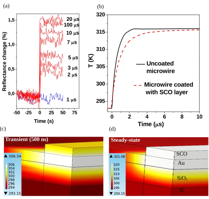
Fig. 3 were acquired with a resolution of ca. 300 nm, but the spatial resolution of the NSOM analysis can be obviously further improved using smaller aperture tips and shorter tip-sample separation during signal acquisition. However, the real bottleneck to increase the spatial resolution is related actually to the thermometer material. One must remind that the spin transition in the particles is first-order and occurs thus by nucleation and growth. When the local temperature is sufficiently high to overcome the nucleation barrier the whole particle -strictly speaking the whole coherent crystalline domain - is transformed to the HS phase in a cooperative manner. Spatial resolution below the particle size is therefore not achievable. Due to the time-temperature integration principle of our thermometer it provides basically no temporal resolution. It is, nevertheless, important to assess how short transient heating can be detected in the device. To examine this question we used a single, sharp (< 25 ns rising and falling edges) current pulse of fixed amplitude (50 mA) and variable length (1 – 100 s). Between two pulses the device was reset to its initial state by cooling it below the hysteresis region. For pulse durations between 10 - 100 s, a reflectivity rise of ca. 1.3 – 1.5 % is observed on the wire (see Fig. 4a), which corresponds to a full conversion of the thermometer to the HS state in the given experimental conditions. For shorter pulses the reflectivity changes become less pronounced and finally no change is observed for a single 1 s pulse. This contrasts with our experimental and simulation data, which show clearly that the microwire reaches its steady-state temperature in ca. 1 s (Fig. S4). The delay between the temperature rise in the wire and the response of the thermometer delay is most probably related to the slow propagation of the heat wave within the SCO layer whose thermal diffusivity is rather low (ca. 10-1 mm2s-1). We have examined this issue using numerical simulations (Fig. 4b-4d) and complementary experiments (Fig. S9), which revealed that the presence of the thermometer layer did not impact much the response time of the gold wire itself, but the thermalization of the SCO material was indeed delayed on the s scale. Obviously, by reducing the film thickness the thermalization times can be improved, but at some point the intrinsic spin-state switching rates will provide a bottleneck. The spin-state interconversion rates far from the bistability region have been extensively studied for a wide range of complexes and the observed rate constants fall between 106 – 109 s-1 near room temperature [15]. On the other hand, some reports indicate a slowdown of the kinetics within the hysteresis region [16]. At this stage it is thus difficult to conclude whether one can expect
a significant improvement of the thermometer response below the s range with SCO compounds by simply reducing their thickness (i.e. the their thermalization time).
-50 -25 0 25 50 75 0,0 0,5 1,0 1,5 100 s 20 s 10 s 7 s 5 s 3 s 2 s R ef le ct an ce c h an g e (% ) Time (s) 1 s 0 2 4 6 8 10 295 300 305 310 315 320 Microwire coated with SCO layer
Uncoated microwire T ( K ) Time (s)
Fig. 4. Temporal detection limit. (a) Optical reflectivity of the microwire device recorded at 385 K
before and after applying (at t = 0) a single square current pulse of 50 mA with different pulse widths (1 – 100 s). (b) Simulated time-resolved thermal response of the microwire in the presence (solid line) and absence (dashed line) of the thermometer material for a 50 mA sharp current step applied at t = 0. (c) Transient (500 ns after the current step) and (d) steady-state simulated 3D temperature distributions around the microwire.
In summary, we have shown that a spin crossover compound exhibiting thermal hysteresis used in conjunction with a scanning probe microscopy technique allows for sub-wavelength resolution imaging of s scale transient heating phenomena – even if this latter occurs in an erratic way. To our knowledge no other nanothermometry method is able to provide such information. As mentioned before some further improvement of the spatial and temporal
(a) (b) (d) (c) Transient (500 ns) Steady-state Si SiO2 Au SCO
detection limits is certainly possible by preparing thinner and more homogenous thermometer films. This would also further reduce the invasiveness of the thermometer material, though at the detriment of the optical contrast. In order to turn our method into a fully-fledged thermometry application the most obvious shortcoming of the presented approach is that it works only in a fixed range of temperatures (between ca. 353 and 393 K). Similar to liquid crystal thermometers, it will be thus necessary to develop a series of bistable nanothermometers with wide hysteresis loops centered at different technologically relevant temperatures. Taking into account the current state-of-the-art in spin crossover research [ 17-23], clearly there is no fundamental obstacle to reach this aim. Of course, other families of phase change materials can be also used besides SCO complexes. Finally, it may be worth to mention that instead of optical readout other approaches, such as quantitative AFM mechanical measurements [24], could be also used to detect the temperature induced changes in the thermometer material – providing in some cases higher sensitivity and spatial resolution.
REFERENCESAND NOTES
1. L. D. Carlos, F. Placio (eds), Thermometry at the Nanoscale: Techniques and Selected
Applications (Royal Society of Chemistry, 2016).
2. C. D. S. Brites et al., Nanoscale 4, 4799 (2012).
3. J. Christofferson et al., J. Electron. Packag. 130, 041101 (2008).
4. D. G. Cahill, K. Goodson, A. Majumdar, J. Heat. Trans. 124, 223 (2002). 5. A. Majumdar, J. P. Carrejo, J. Lai, Appl. Phys. Lett. 62, 2501 (1993). 6. F. Menges, H. Riel, A. Stemmer, B. Gotsmann, Nano Lett. 12, 596 (2012). 7. M. Mecklenburg et al., Science 347, 629 (2015).
8. Y.-K. Tzeng et al., Nano Lett. 15, 3945 (2015).
9. M. Farzaneh et al., J. Phys. D: Appl. Phys. 42, 143001 (2009). 10. A. Csendes, V. Székely, M. Rencz, Microel. Eng. 31, 281 (1996). 11. C. M. Quintero et al., Microel. J. 46, 1167 (2015).
12. J. Kröber et al., Chem. Mater. 6, 1404 (1994). 13. A. Grosjean et al., Eur. J. Inorg. Chem. 796 (2013).
14. P. R. N. Childs, J. R. Greenwood, C. A. Long, Rev. Sci. Instrum. 71, 2959 (2000). 15. A. Hauser, Top. Curr. Chem. 234, 155 (2004).
16. G. Galle et al., Chem. Phys Lett. 500, 18 (2010).
17. M. Carmen Munoz, J. A. Real, Coord. Chem. Rev. 255, 2068 (2011). 18. P. Gütlich, A. B. Gaspar, Y. Garcia, Beilstein J. Org. Chem. 9, 342 (2013). 19. H. J. Shepherd, et al., Eur. J. Inorg. Chem. 653 (2013).
20. I. Salitros et al., Monatsh.Chem. 140, 695 (2009). 21. O. Roubeau, Chem. Eur. J. 18, 15230 (2012).
22. M. Cavallini, Phys. Chem. Chem. Phys. 14, 11867 (2012).
23. Spin-Crossover Materials, M. A. Halcrow (ed.), John Wiley & Sons, Oxford, UK, 2013. 24. E. M. Hernández et al., Adv. Mater. 26, 2889 (2014).
This work was supported by the Agence National de la Recherche (ANR-10-NANO-012–02), the French RENATECH network, the French Embassy in Ukraine and the LIA France-Mexico. We thank D. Manrique and M. Lopes from LCC for experimental help.
SUPPLEMENTARY MATERIALS
SUPPLEMENTARY MATERIALS
High spatial resolution imaging of transient thermal events
using materials with thermal memory
Olena Kraieva1,2, Carlos M. Quintero2, Iurii Suleimanov1,3, Edna M. Hernandez1,4, Denis Lagrange2, Lionel Salmon1, William Nicolazzi1, Gábor Molnár1,*, Christian Bergaud2,* and Azzedine Bousseksou1,*
* Corresponding authors. E-mail: [email protected], [email protected],
1LCC, CNRS & Université de Toulouse, UPS, INP, F-31077 Toulouse, France. 2LAAS, CNRS & Université de Toulouse, INSA, UPS, F-31077 Toulouse, France. 3Department of Chemistry, Taras Shevchenko National University of Kyiv, Kyiv, Ukraine. 4Facultad de Ciencias, Universidad Nacional Autónoma de México, Mexico City, Mexico.
1. Sample synthesis and characterization
2. Microwire heater fabrication
3. Steady-state thermal characterization of microwire heaters
4. Transient thermal characterization of microwire heaters
5. Finite element simulations of the temperature distribution in the microwires
6. Construction of temperature maps of transient thermal events
7. NSOM experiments
1. Sample synthesis and characterization
An aqueous solution of Fe(BF4)2·6H2O (211 mg, 0.625 mmol in 0.5 mL H2O) was added dropwise to a mixture of 1.8 mL of Triton X-100, 1.8 mL of hexanol and 7.5 mL of cyclohexane. Then, a solution of H-trz (131 mg, 1.87 mmol in 0.5 mL H2O) was added dropwise to another Triton – hexanol – cyclohexane mixture with the same composition. The two microemulsions were quickly combined. The mixture was stirred for 24 h, followed by addition of ethanol to destroy the structure of the microemulsion. The nanoparticles (Fig. S1) were recovered by centrifugation, washed three times with ethanol and dried at 70 ºC for 12 h. 50 mg of this powder was disaggregated with ultrasonic treatment and mechanically dispersed in 2 ml absolute EtOH. This dispersion was then spin-coated (speed 4500 rpm, acceleration 4000 rpm/sec, duration 30 sec) on a clean chip with microwires.
Figure S1: SEM (left) and TEM (right) pictures of the [Fe(Htrz)2(trz)]BF4 particles
2. Microwire heater fabrication
The microwires were fabricated by means of photolithography both on oxidized (650 nm SiO2) silicon substrates. A negative photoresist (nLOF) was spin coated and exposed to UV radiation through an appropriate mask in order to pattern the wires and the electrodes in the same time. The patterns were revealed in a 1:1 mix of NLOF developer solution and de-ionized water. After this, metallization (Ti and Au of 10 nm and 350 nm, respectively) was performed, followed by lift-off in acetone. Each chip contains several wires that vary in length from 1 to 2 mm and in width from 2 to 8 m (Fig. S2). The geometry of the device was controlled using SEM, profilometry and ellipsometry.
3. Steady-state thermal characterization of microwire heaters
All electrical characterizations and measurements were carried out by applying current (i.e. not voltage) bias in order to guarantee always a reproducible current excitation and associated Joule heating. The thermal variation induced by the current bias generates a delta of resistance
ΔR in the wire proportional to the temperature change ΔT that can be described as:
∆ R=R0α0∆ T , where R0 is the resistance of the heater and α0 the linear temperature
coefficient of electrical resistance at the temperature of measurement T0. The temperature difference ΔT is an averaged value of the ΔT induced in the whole wire. The variation of the resistance of the wires at low bias current was measured in 4-probe configuration as a function of the temperature between 293 and 353 K using a Kethley 6430 source-meter and a heating-cooling stage and the value of α0 was calculated (typically 0.0026 K-1). In a second
time, the resistance of each heater was determined as a function of the applied electrical current bias while keeping the temperature of the stage fixed at 293 K. Assuming that the variations of the measured resistance for each wire come primarily from the temperature change of the wire, a relationship between I and T was finally established (Fig. S3).
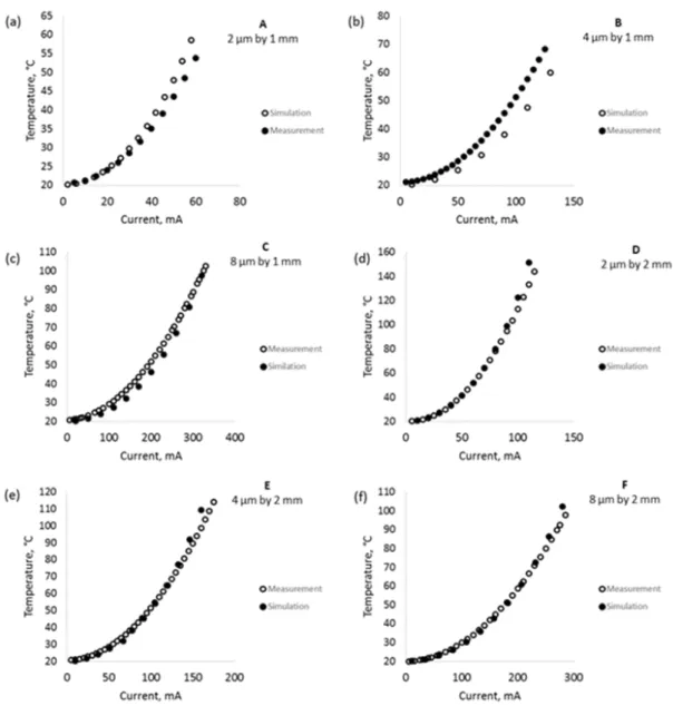
Figure S3. Calibration curves of the microwires with 1 mm length and 2 µm (A), 4 µm (B) and 8 µm (C) widths, as well as with 2 mm length and 2 µm (D), 4 µm (E) and 8 µm (F) widths. For each wire both the experimental and numerical simulation data are shown.
4. Transient thermal characterization of microwire heaters
To monitor electrically the transient heating of the wires, we implemented a transient differential resistance measurement (see ref. [11] for details). Briefly, this custom-built setup sends sharp current steps (rising time ≤ 25 ns) to the heater under study ( Rh ) and a reference resistance ( Rref ) of identical value as the heater (at small bias) and negligible α.
The output of the circuit is an amplified version of the voltage difference Vdiff=Vh−Vref
between the voltage on the heater and the voltage on the reference resistance. Since Rref
will remain unchanged independently of the applied current, the signal Vdiff will be a scaled version of the ΔT induced on the wire due to Joule heating. As it was noted above we used a current (and not voltage) pulse in order to provide a known excitation to the heaters even if the resistive paths around them are different. The output voltage difference Vdiff as
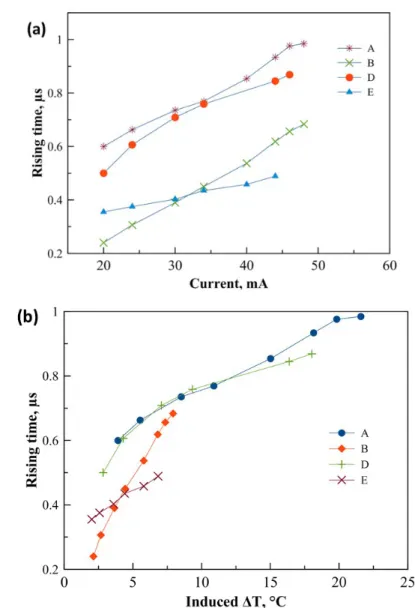
well as the voltage measured on the wire under study and on the reference resistance were recorded by a Tektronix oscilloscope (bandwidth 100 MHz). As shown in Fig. S4 the thermal rise time of the devices in our operating conditions fall in the sub-microsecond range.
Figure S4. Thermal rising time of 4 different microwires as a function of (a) the amplitude of the applied current step and (b) the induced temperature variation determined from differential resistance measurements. The Si substrate was held at 293 K.
5. Finite element simulations of the temperature distribution in the microwires
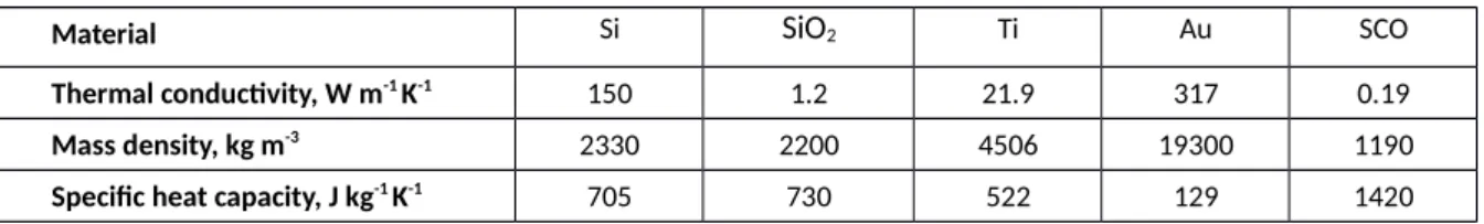
The 3D steady-state and transient temperature distributions in the devices were simulated using the finite element method (FEM) by numerically solving the heat equation as implemented in the software package COMSOL (‘Joule Heating’ and ‘Heat Transfer’ modules). Due to the small heating area and the relatively narrow temperature range covered (293 – 403 K), the radiation losses were considered negligible. This left us with a simplified thermal description of the system, which largely depends on the power input for the heat generation via Joule heating in the metallic wire, the thermal properties of the materials (see
Table S1) and the system boundary conditions for the power losses. Since the relevant thermal properties of the SCO layer of 1 are not known this layer was modelled by an equivalent thickness of PMMA (Poly(methyl-methacrylate)), which is expected to display similar thermal diffusivity as 1. This approximation is corroborated by the very satisfactory agreement between the experiments and the numerical simulations. Further confirmation can be inferred from the data in Fig. 4a. By considering the thickness L of the SCO layer (ca. 300 nm) and the characteristic thermalization time (ca. 1-10 s) depicted in this figure one can roughly estimate the thermal diffusivity as D = L2/ = 10-1 – 100 mm2/s, which is of the same order of magnitude than that of PMMA. When analyzing the simulated 3D temperature distribution in the heaters, we were particularly interested in the confinement of the temperature obtained in the metallic part of the device as well as the temperature gradient in the thermometer layer. Overall we have found that the temperature in the wires is very uniform and the added thermal load of the SCO layer did not perturb significantly the steady-state heat distribution in the device (see Fig. 1d). The transient analysis in COMSOL was performed by applying a current step of a few ms with a rise and decay edge of 4 ns. The corresponding function in the COMSOL library is a smoothed Heaviside function with a continuous second derivative without overshoot (flc2hs). The FEM simulation of the transient thermal response of a microwire is extremely time and computation resources consuming. Therefore, we have simulated the time response of only one microwire (A) with dimensions of 350 nm height, 2 µm width and 1 mm length. Calculations were performed both with the uncoated and coated (300 nm SCO layer) microwire. Representative results are shown in
Figures 4b and 4c. We observe ca. 1.01 s rise time for the clean wire for 50 mA excitation, which compares nicely with the experimental value (0.98 s) shown in Fig. S4a. The thermal load of the SCO layer slows down the system and the rise time increases to ca. 1.75 µs (for the same excitation).
Table S1. Material parameters used in COMSOL Multiphysics simulations (T = 20 °C)
Material Si SiO2 Ti Au SCO
Thermal conductivity, W m-1 K-1 150 1.2 21.9 317 0.19
Mass density, kg m-3 2330 2200 4506 19300 1190
Specific heat capacity, J kg-1 K-1 705 730 522 129 1420
6. Construction of temperature maps of transient thermal events
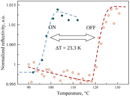
The principle of the temperature measurement is as follows. First, the reflectivity of the device in the OFF state is determined as a function of T for selected regions of interest, ROIs (for example, for each pixel of the CCD camera or for binned pixels). In a second step the same measurement is repeated, but at each temperature the device is switched to the ON state before the acquisition of the reflectivity signal. The difference between the apparent transition temperatures in the two cases (i.e. ON and OFF states) accounts for the heating induced by
the device operation. This protocol is illustrated in Fig. S5 wherein the device was operated by a current pulse of 50 mA amplitude and 50 µs duration. The averaged difference between the transition curves in the OFF and ON states in this case is 23.3 ± 0.2 K. By repeating this calibration for each pixel maps of the transient temperature changes can be constructed (Fig. 2c-2d).
Figure S5. Open symbols: Variation of the reflectivity signal of the microwire A as a function of the temperature (heating mode) in the OFF state of the device. Closed symbols: the same experiment, but at each temperature step the device was switched to the ON state by a current pulse (50 µs, 50 mA) before the reflectivity measurement. Dashed lines were inserted to guide the eye.
7. NSOM experiments
The set-up for combined far-field and near-field optical reflectivity measurements is based on a Nanonics Multiview 2000 AFM-NSOM instrument. For far-field reflectivity detection the sample was illuminated with a halogen lamp through a ×20 magnification / 0.4 numerical aperture objective and the light reflected by the sample was detected by a CCD camera (Clara, Andor Technology). For near-field reflectivity measurements a blue line (488 nm) of an argon ion laser was coupled to an NSOM tip fiber. The evanescent waves produced at the fiber aperture (ca. 70 nm) and diffracted by the sample were collected by the microscope objective in far-field and detected by a photomultiplier tube. A combination of bandpass filters and beamsplitters were used to separate light from the halogen lamp and the laser. For imaging purposes the NSOM was operated either in AFM feedback or in constant-height mode ca. 60 nm above the surface, which was determined from preliminary AFM scans. While the former method provides better spatial resolution, the latter approach is less invasive.
Since the laser irradiation used to acquire NSOM images can also contribute to the heating of our thermometer material we have first carried out a series of experiments to determine the threshold power. As shown in Fig. S6, below ca. 2 mW power the laser-induced heating is negligible. In the next step simultaneous far-field and near-field reflectivity experiments were carried out with the thermometer material deposited on the microwire heaters. These experiments (Fig. 3, Fig. S7 and Fig. S8) show basically the same results, i.e. an optical reflectivity increase tightly confined to the heated wire.
OFF ON
Figure S6. Left panel: Far-field reflectivity change of a film of 1 following NSOM scans with different laser powers. Right panel: The corresponding reflectivity images. They were recorded after scanning the surface with an NSOM tip using different laser powers (as indicated in the figures). The initial image (i.e. before the NSOM scan) was subtracted. The yellow rectangle marks the area scanned by NSOM. During the experiments the temperature of the substrate was held ca. 2-3 K below the spin transition temperature.
Figure S7. (a) Fear-field and (b) NSOM reflectivity images of a film of 1 deposited on a gold microwire. The images were acquired at 378 K before and after applying a 190 mA current pulse through the wire. The reflectance difference induced by the current pulse (images and cross-sections) are shown in (c) for the far-field and in (d) for the NSOM experiments. The local heating associated with the current pulse induces a reflectivity increase of ca. 6 % and 30 % in the far-field and near-field experiments, respectively.
Figure S8. (a) Fear-field images of 1 deposited on a gold microwire acquired at 378 K before and after applying a 92 mA current pulse through the wire. (b) The far-field reflectance difference induced by the current pulse (image and cross-section). (c) NSOM images of 1 deposited on a gold microwire acquired at 378 K before and after applying a 92 mA current pulse through the wire. The corresponding cross sections are also shown. (d) The NSOM reflectance difference induced by the current pulse (image and cross-section).
8. Thermalization time
To assess the thermalization rate of our SCO thermometer layer an experiment was carried out wherein we applied to a microwire 10 current pulses of 1 s duration and 50 mA amplitude while keeping the substrate at 374 K. Fig. S9 shows the results obtained when reducing the delay between the pulses from 3.0 to 1.3 s. For the longest delay no change is observed, i.e. the pulses are “independent”. When reducing the delay to 2 s, a reflectivity change is observed, which becomes more and more pronounced for shorter delays. In other words, heat
d) c)
accumulates progressively during the pulses. This experiment indicates that heat diffusion time in the SCO layer is of the order of a few s in our experimental conditions.
Figure S9. Optical reflectivity of the microwire device (same device as in Fig. 4) recorded at 374 K
before and after applying 10 current pulses (50 mA, 1 s) with different pulse delays (1.3 – 3.0 s).
The effect of heat accumulation on the spin state of the thermometer nanoparticles during this experiment is also shown.