HAL Id: hal-01887185
https://hal.archives-ouvertes.fr/hal-01887185
Submitted on 3 Oct 2018
HAL is a multi-disciplinary open access
archive for the deposit and dissemination of
sci-entific research documents, whether they are
pub-lished or not. The documents may come from
teaching and research institutions in France or
abroad, or from public or private research centers.
L’archive ouverte pluridisciplinaire HAL, est
destinée au dépôt et à la diffusion de documents
scientifiques de niveau recherche, publiés ou non,
émanant des établissements d’enseignement et de
recherche français ou étrangers, des laboratoires
publics ou privés.
A sub-100nW Power Supply Unit Embedding
Untrimmed Timing and Voltage References for
Duty-Cycled µW-Range Load in FDSOI 28nm
Anthony Quelen, Franck Badets, Gaël Pillonnet
To cite this version:
Anthony Quelen, Franck Badets, Gaël Pillonnet.
A sub-100nW Power Supply Unit Embedding
Untrimmed Timing and Voltage References for Duty-Cycled µW-Range Load in FDSOI 28nm. 47th
European Solid-State Device Research Conference ESSCIRC 2017, 2017, Louvain, Belgium.
�hal-01887185�
A sub-100nW Power Supply Unit Embedding
Untrimmed Timing and Voltage References
for Duty-Cycled µW-Range Load in FDSOI 28nm
Anthony Quelen, Franck Badets, Gaël Pillonnet
Univ. Grenoble Alpes, F-38000 Grenoble, France CEA, LETI, MINATEC Campus, F-38054 Grenoble, Francegael.pillonnet@cea.fr
Abstract—The paper proposes a power supply unit to efficiently supply always-on or duty-cycled IoT loads which consumes in µW-range. This PS achieves the highest 93% and 99% current efficiencies at average output currents of 1µA and 100µA to date, respectively. This unit includes a voltage reference and oscillator to generate autonomously duty-cycled power delivery operation as low as a 30µs on-period. The overall power supply unit exhibits sub-100nA quiescent current and provides a regulated 0.92V power rail with less than 10% variation against temperature, process and input supply range and without trimming. Fully integrated in FDSOI 28nm, the die area is
0.036mm2 showing a compact and untrimmed solution to supply
small die area IoT node in SoC context without any off-chip components.
Keywords— duty-cycled voltage regulator, silicon-based oscillator, voltage reference and micro-power management.
I. INTRODUCTION
To allow a few years’ operation using a button battery, the average total power consumption of sensor node must be in the µW range. Duty-cycled operation is also essential for extending system lifetime: during short periods of activity, the system performs sensing, processing and communication before going back to deep sleep-mode. This duty-cycled operation requires a power supply unit (PSU) to provide clean power rails during the short sensor activity time. Therefore this paper proposes a PSU to efficiently supply always-on or duty-cycled IoT loads which consume in µW-range. Even if nW range oscillators (OSC) [1], duty-cycled voltage references (VREF) [2,7] and various always-on mW range low drop-out (LDO) regulators [3-6] have been reported, a complete PSU allowing low duty-cycled mode (DCM), few µs awake time, µA quiescent current, mV voltage drop during line and load transients, and a few % voltage accuracy against battery voltage and PVT variations has not yet been covered in the literature. This paper is composed into five parts which describe the PSU at system-level, give some design details and silicon characterization of the three main PSU integrated functions i.e. oscillator, voltage reference and voltage regulator, and the measured PSU performance against various load and duty-cycle operation.
II. PROPOSED POWER SUPPLY UNIT
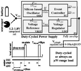
As depicted in Fig. 1, a 0.036mm2 PSU is proposed which
embeds a silicon-based oscillator, VREF and LDO regulators fully-integrated in 28nm FDSOI technology featuring sub-100nW quiescent current in DCM. This ad hoc power management unit is dedicated to µW DCM loads such as wake-up radio, volatile memory and microcontroller. The always-on 50nW OSC provides the time references to periodically refresh the voltage reference e.g. typically at 5% rate and to independently wake-up the LDO when the load is in active mode. Typically each 40ms, the VREF is turned-on, sampled and held to maintain the LDO reference voltage. The LDO is started-up in 1µs and can deliver up to 100µA output current under 0.92V with ±5% voltage accuracy from unregulated 1.2-1.8V input voltage during an on-period as short as 30µs.
Fig. 1. Block diagrams of duty-cycled PSU to supply a µW load
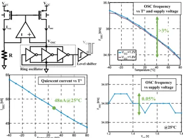
III. SILICON-BASED OSCILLATOR
Fig 2. depicts the always-on oscillator which is based on the architecture which has been first disclosed in [6]. This architecture presents two main advantages towards the implementation of ultra-low-power (ULP) stable silicon-based
oscillator. First, this architecture is comparator-free and thus, will not suffer from its poor offset and delay stabilities. Second, this architecture is self-biased prone. As there is no need of voltage or current reference, this architecture is well suited towards ULP implementations. Moreover, it reduces the number of sources of temperature instability.
Basically, the oscillator consists in an active current mirror that biases a resistor R in a first branch and a ring oscillator (RO) in a second branch. The amplifier ensures that the RO DC resistance will track the resistance of R. It could be easily demonstrated that the RO DC resistance RRO is equal to:
C f R RO RO 1 = (1)
where C is the total capacitance load of the RO, and fRO its
oscillation frequency.
Therefore, as the RO DC resistance tracks R, the frequency of the oscillator depicted in Fig. 2 is given by:
RC fRO
1
= (2)
It is apparent from (2) that the frequency stability mainly relies on the temperature stability of the 180ppm/°C temperature coefficient resistor R.
Moreover, the amplifier ensures equal voltages across the resistor and ring oscillator DC bias, and also ensures good voltage supply immunity as explained in [1].
As shown in Fig. 2, the OSC frequency is set to 35kHz allowing as low as a 30µs on-period for LDO. Temperature and power supply stabilities of ±1.5% have also been achieved from 40°C to 80°C and 1.2 to 1.8V, respectively. The oscillator power consumption has been measured at 48nW under a 1.2V power supply. The current consumption of a resistor branch, RO, and amplifier are 20, 20 and 10nA, respectively. A 1.5nA level shifter drives the event-controller composed of a few flip-flop gates which wake up the VREF and LDO blocks periodically at a programmable rate.
1.2 1.4 1.6 1.8 34.93 34.95 34.97 VCC [V] FOS C [k H z] -40 -20 0 20 40 60 80 34.5 35 35.5 Temperature [°C] FOSC [k H z] VCC=1.2V VCC=1.8V -40 -20 0 20 40 60 80 45 50 55 Temperature [°C] IOSC [n A] OSC frequency vs T° and supply voltage
Quiescent current vs T° OSC frequency
vs supply voltage 48nA@25°C >3% 0.05% @25°C Ires VCC +
-VCC Iosc Ring oscillator VOSC Level shifter VCC 0 RFig. 2. Results of 50nA 35kHz Silicon Oscillator (OSC)
IV. UNTRIMMED AND DUTY-CYCLED VOLTAGE REFERENCE
The untrimmed duty-cycled VREF is shown in Fig. 3 including a sample and hold for DCM. VREF is resistor-less BJT-less topology to save silicon area. It is composed of a current generator which biases two stacked PTAT’s and diode-connected transistors to generate 0.92V.
The combination of PTAT and CTAT using different device flavors i.e. thin/thick oxides and low/regular threshold voltages cancels the PVT dependence. VREF sensitivity is equal to σ=0.55%@25°C across 10 dies without trimming across 1.2-1.8V input voltage. Moreover, the polarization scheme keeps a constant current consumption vs. temperature achieving less than 100nA at 80°C in always-on mode. As the average power of a VREF greatly depends on achievable DCM, the reference voltage VREF_SH is maintained in the sample and hold capacitor CSH when the VREF is disabled. The sleep-mode duration is limited to 40ms to maintain 7% voltage accuracy on VREF_SH. Using a 2ms on-period i.e. 5% duty-cycled, the average current consumption is 5nW@1.2V. Compared [2], the always-on power consumption of VREF is reduced by two decades and the die occupies 10x less area.
1.2 1.4 1.6 1.8 99.95 100 100.05 Supply voltage Vcc [V] -40 -20 0 20 40 60 80 0.86 0.88 0.9 0.92 Temperature [°C] VRE F-S H [V ] 100% 70% 30% 5% Voltage reference vs temperature and duty cycle
Voltage reference (normalized %) vs supply voltage 7% 0.05% DCVREF CLP 25pF VREF VREF_SH
All back-gate are connected to ground VCC=1.2-1.8V gnd rvt lvt lvt lvt
Current Generator Double Stacked PTATCTAT Sample & hold
I=20nA
ENREF
ENREF
I I
I
I Transistors disabling VREF are not represented
Fig. 3. Results of the duty-cycled voltage reference (VREF)
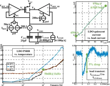
V. DUTY-CYCLED VOLTAGE REGULATOR
While the on-chip integrated capacitor is only 25pF, the proposed duty-cycled LDO (Fig. 4) is able to deliver up to 100µA with an input voltage between 1.2V and 1.8V in the 0 to 800pF range. The quiescent current (no load) is 450nA in always-on operation excluding the current bias generator (200nA).
To extend its capability in order to be stable under large capacitive load range and zero to full load current, the regulator has two feedback loops to modulate both gate and back bias voltages simultaneously which is a potential and interesting feature brought by the FDSOI technology compared to a bulk technology. Firstly, the FDSOI back-biasing allows higher dynamic voltage range (-/+2V) than in bulk technology (<VTH),
three times higher than the bulk counterpart (25mV/V). Compared to [8], we are no limited by reverse inherent bulk body diode and we introduce a variable current bias controlled by the delivered LDO current.
At low load current, the back-biasing feedback offer a faster but lower DC gain than the gate loop, therefore, a zero is introduced at the frequency where the gain of the two loops are equal. This allows to compensate the low output pole in frequency due to the load capacitor, and by this way, to increase the maximum output capacitor range where the LDO is stable.
Moreover, the proposed additional back biasing loop improves to the transient response from no/low load current to high load current. At high load current, the variable current biasing of the gate’s feedback amplifier increases the bandwidth according to the output current ILOAD to break the
trade-off between transient response and efficiency depending on speed and quiescent current, respectively, without compromising stability. At high current load, the gate feedback loop becomes faster than the back-biasing loop, but as the output pole is also at higher frequency due to the lower power transistor output impedance, then no additional zero is required to stabilize.
Fig. 4 shows quiescent current versus load current, demonstrating a working adaptive-biasing scheme. The PSRR is lower than 50dB below 1 kHz frequency. LDO regulates the output voltage against load transient as also shown Fig. 4. The 0.92V power rail experiences less than 5 and 10% undershoot for a half- and full-load transients, respectively. Used with a 100µW wake-up radio load we measure less than 1% undershoot. The LDO has a DCM mode independent of VREF, wakes-up in 1µs as shown in the left graph of Fig. 5. The quiescent current including VREF slightly depends on temperature (Fig. 5) and is lower than 1µA @25°C.
-0.1 0 0.1 0.2 0.3 0.85 0.9 0.95 time [µs] VLO A D [V ] VCC 50nA A 200:1 + gnd gnd + -VREF_SH + -IBG IBB 200nA VREF_SH gnd VG VB VLDO CINT 25pF CLOAD [0-800pF] ILOAD [0-100µA] IREF 0 20 40 60 80 0.5 0.7 0.9 ILOAD [µA] ILDO [µ A] LDO quiescent current vs. load current 100 102 104 -70 -60 -50 -40 -30 -20 -10 Frequency [Hz] PSR R 25°C -40°C 80°C LDO PSRR vs. temperature 450nA 970nA @full load
50dB@1kHz load transient: ILOAD,max/2 to
ILOAD,max
5% drop
Fig. 4. LDO schematic, quiescent current and dynamic performance
-2 -1 0 1 0 0.2 0.4 0.6 0.8 1 Time [µs] Vo ltag e [V ] ENLDO VLDO -40 -20 0 20 40 60 80 0.9 1 1.1 1.2 Temperature [°C] IREF +ILD O [µ A] DC REF=100% DCREF=5%
REF+LDO quiescent currents vs DCREF@ {DCLDO=100%, ILOAD=100µA}
0.98µA@25°C
LDO startup
1µs
Fig. 5. LDO startup and LDO+VREF quiescent current vs temperature
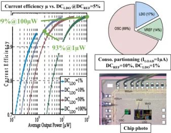
VI. POWER SUPPLY UNIT OVERALL PERFORMANCE
Fig. 6 shows PSU efficiencies from 1 to 100% duty-cycle with always-on OSC, refreshed VREF and LDO providing 1 to 100µA. The current efficiency is expressed as:
(3) where IOUT is the load current, IOSC, IVREF and ILDO are the
OSC, VREF and LDO quiescent current respectively, IVREF is
the VREF quiescent current reduced by 0.05 factor as the REF is duty-cycled with 5% on-cycle, and DCLDO is the LDO
duty-cycled ratio.
Current and average power efficiencies (@100µA during 200µs on-period, 1% DCM, Vcc=1.2V) are 99 and 76%, respectively, including OSC, VREF and LDO. Compared to prior works [3-6] (Table 1), the quiescent current is order of magnitude lower with smallest die occupation, without any external capacitor, a large input voltage range capability, including voltage reference and timer to self-manage duty cycle operation. The current efficiency is extend to 99% meaning x4 power reduction factor compared to the best in class voltage regulator. Compared to fully-integrated power supplies dedicated to high-density digital SoC [9], the power density (Watt delivered per Si area) is dramatically lower but the primarily objective is the power efficiency here.
The power consumption distribution is also shown in Figure 6. The PSU set-point voltage is 0.92V and varies by 10% without trimming phase against PVT variations and under the line and load variations. The PSU operating with a supply ranging from 1.2 to 1.8V is compatible with various button batteries or unregulated output of a harvester interface.
10-1 100 101 102 0.7
0.8 0.9 1
Average Output Power [µW]
C ur re nt E ff ici en cy DC LDO=1% DCLDO=10% DC LDO=30% DC LDO=100%
Current efficiency µ vs. DCLDO@DCREF=5%
93%@1µW
OSC (69%) VREF (14%)
LDO (17%)
Conso. partionning (ILOAD=1µA)
DCREF=10%, DCLDO=1%
Chip photo
99%@100µW
Fig. 6. Results for the entire duty-cycled power supply unit
VII. CONCLUSIONS
The proposed PSU exhibits the highest 99% and 93% current efficiencies at 100µ and 1µA load currents compared to prior works. Moreover, the LDO has the ability to be duty-cycled for as low as a 30µs on-period exhibiting sub-100nA average quiescent current including the timer and voltage/current references. The die area is 0.005, 0.017, 0.014mm2 for the OSC, VREF and LDO, respectively,
showing a compact and untrimmed solution to supply small die area node in µW-range without any off-chip capacitor.
ACKNOWLEDGMENT
This work has been performed in the THINGS2DO project (JTI Contract Number 621221), co-funded by grants from France and the ECSEL Joint Undertaking.
REFERENCES
[1] D. Ruffieux, A. Pezous, A. C. Pliska, and F. Krummenacher, “Silicon-resonator-based, 3µA real-time clock with +/-5ppm frequency accuracy,” in 2009 IEEE International Solid-State Circuits Conference (ISSCC), 2009, p. 210–211,211a.
[2] Y. P. Chen, M. Fojtik, D. Blaauw, and D. Sylvester, “A 2.98nW bandgap voltage reference using a self-tuning low leakage sample and hold,” in 2012 Symposium on VLSI Circuits (VLSIC), 2012, pp. 200– 201.
[3] Y. H. Lam and W. H. Ki, “A 0.9V 0.35µm Adaptively Biased CMOS LDO Regulator with Fast Transient Response,” in 2008 IEEE International Solid-State Circuits Conference (ISSCC), 2008, pp. 442– 626.
[4] W. C. Chen, Y. P. Su, Y. H. Lee, C. L. Wey, and K. H. Chen, “0.65V-input-voltage 0.6V-output-voltage 30ppm/°C low-dropout regulator with embedded voltage reference for low-power biomedical systems,” in 2014 IEEE International Solid-State Circuits Conference (ISSCC), 2014, pp. 304–305.
[5] S. B. Nasir, S. Gangopadhyay, and A. Raychowdhury, “A 0.13µm fully digital low-dropout regulator with adaptive control and reduced dynamic stability for ultra-wide dynamic range,” in 2015 IEEE International Solid-State Circuits Conference (ISSCC), 2015, pp. 1–3.
[6] D. Kim and M. Seok, “Fully integrated low-drop-out regulator based on event-driven PI control,” in 2016 IEEE International Solid-State Circuits Conference (ISSCC), 2016, pp. 148–149.
[7] Y. Osaki, T. Hirose, N. Kuroki, and M. Numa, “1.2-V Supply, 100-nW, 1.09-V Bandgap and 0.7-V Supply, 52.5-nW, 0.55-V Subbandgap Reference Circuits for Nanowatt CMOS LSIs,” in IEEE Journal of Solid-State Circuits (JSSCC), vol. 48, no. 6, pp. 1530–1538, Jun. 2013. [8] K. Keikhosravy and S. Mirabbasi, “A 0.13-µm CMOS Low-Power
Capacitor-Less LDO Regulator Using Bulk-Modulation Technique,” in IEEE Transactions on Circuits and Systems I: Regular Papers (TCASI), vol. 61, no. 11, pp. 3105–3114, Nov. 2014.
[9] G. Pillonnet and N. Jeanniot, “Effect of CMOS Technology Scaling on Fully-Integrated Power Supply Efficiency,” in 9th International
Conference on Integrated Power Electronics Systems, 2016, pp. 1–5.
TABLE I. POWERSUPPLYUNITCOMPARISON
Conditions [3] [4] [5] [6] Proposed Unit
Technology 350nm bulk 21nm bulk 130nm bulk 65nm bulk FDSOI 28nm -
Embedded Voltage Reference No Yes No No Yes -
Wake-up Timer No No No No Yes -
Input Voltage 1.05 0.65-0.9 0.5-1.2 0.5-1 1.2-1.8 V
Output Voltage 0.9 0.6 0.45-1.14 0.45 -0.95 0.92 V
Max. Output current 50 10 4.6 3.5 0.1 mA
Output Capacitor 1000 <0.1 1 4 0-0.8 nF
Quiescent Current
always-on
lower-load 4.04 5 24 12.5 0.8 (1) µA
5% duty-cycled
2ms on-period, no-load N.A. N.A. N.A. N.A. 0.09 (1) µA
Current Efficiency @100µA, 100% DCLDO 95.7 - 80 85 99
(1) %
@1µA, 1% DCLDO - - - - 93.3 (1) %
Line Regulation full load 1.1 16 - - 0.2 mV/V
Area 0.053 (2) 0.015 0.114 0.029 0.014
0.036 (1) mm 2