Analysis and Characterization of Random Skew
and Jitter in a Novel Clock Network
by
Vadim Gutnik
Bachelor of Science, Electrical Engineering and Computer Science,
and Materials Science and Metals Engineering,
University of California at Berkeley (1994)
Master of Science, Electrical Engineering and Computer Science,
Massachusetts Institute of Technology (1996)
Submitted to the Department of Electrical Engineering and Computer
Science
in partial fulfillment of the requirements for the degree of
Doctor of Philosophy in Electrical Engineering
at the
MASSACHUSETTS INSTITUTE OF TECHNOLOGY
June 2000
@
Massachusetts Institute of Technology 2000. All rights reserved.
Author
Department of Electrical Cneering
*Wt
MASSACHUSETTS INSTITUTE OF TECHNOLOGY ~.j-O%JUN 2 2 2000
... .... LIBRARIESand Computer Science
March 3, 2000
C ertified by...
..
...
Anantha Chandrakasan
Accepted by ...
Associate- P9essor of Electrical Engineering
-S
ervisor
Arthur C. Smith
Chairman, Departmental Committee on Graduate Students
Analysis and Characterization of Random Skew and Jitter in
a Novel Clock Network
by
Vadim Gutnik
Submitted to the Department of Electrical Engineering and Computer Science on March 3, 2000, in partial fulfillment of the
requirements for the degree of Doctor of Science in Electrical Engineering
Abstract
System clock uncertainty, in the form of random skew and jitter, is beginning to affect performance of large microprocessors significantly. Process and environmental variations and inter-signal coupling on a chip contribute significant delay variations in long clock lines, and these variations are predicted to make the now widely-used clock tree distribution untenable. Distributed clock generation may allow clock networks to continue scaling with advances in semiconductor processing technology.
A novel clock network composed of multiple synchronized phase-locked loops is
an-alyzed, implemented, and tested. Undesirable large-signal stable (modelocked) states dictate the transfer characteristic of the phase detectors; a matrix formulation of the linearized system allows direct calculation of system poles for any desired oscillator configuration. The circuits were fabricated in CMOS, and two implementations of the system - a 4 oscillator proof-of-concept 400MHz network, and a 16-oscillator,
1.3GHz network network are presented.
A flash time-to-digital converter is presented that exploits parallelism to get
pre-cise time measurements with resolution much smaller than a single gate delay. Unfor-tunately, an unrelated failure precluded measurements on the 16-oscillator chip where the measurement system was integrated, but the principle is shown to be valid on an independent test chip.
Thesis Supervisor: Anantha Chandrakasan
Acknowledgments
I would like to thank my thesis advisor, Professor Chandrakasan for innumerable
technical discussions, for always being available and approachable, and for making sure I could concentrate on thesis work. Thanks also to my thesis readers Professors Boning and Verghese for their help in organizing the thesis.
Thanks goes to my research group as well; my research would have been much less enjoyable and much less successful were it not for their advice, help, and camaraderie. And of course, thanks to my family for putting up with me through an awful lot of years of school.
Contents
1 Clocks in Digital Systems
1.1 D efinitions . . . . 1.2 T hesis Scope . . . .
2 Models of Clock Network Timing Variations
2.1 Previous Work: Clocks ...
2.1.1 Equipotential Clocking . . . . 2.1.2 H-Trees and Generalized Trees . . . .
2.1.3 Active Skew Management . . . . 2.2 Previous Work: Variations . . . . 2.2.1 Layout-Dependent Processing Variations . . .
2.2.2 Wafer-Scale and Random Physical Variations
2.2.3 Circuit Implications of Mismatch . . . . 2.2.4 Abstract Variation Models . . . .
2.3 Categories of Mismatch . . . . 2.4 Clock Architecture Comparison . . . . 2.4.1 Clock m etric . . . . 2.4.2 T ree . . . . 2.4.3 G rid . . . . 2.4.4 Active Feedback . . . .
3 Synchronization and Stability
3.1 Previous Work: Synchronization . . . . 15 15 21 23 . . . . 23 . . . . 24 . . . . 25 . . . . 27 . . . . 27 . . . . 28 . . . . 28 . . . . 29 . . . . 31 . . . . 32 . . . . 35 . . . . 35 . . . . 36 . . . . 39 . . . . 42 49 49
3.1.1 Local Data Synchronization
3.1.2 Local Clock Synchronization
3.2 Proposed Clock Architecture . . . . 3.3 Small Signal 3.3.1 3.3.2 3.4 Large General Derivation . Examples . . . . Signal: Mode Locking
4 Implementation and Testing 4.1 4 Oscillator Chip . . . . . 4.1.1 Oscillator . . . . . 4.1.2 Phase Detector . . 4.1.3 Loop Filter . . . . 4.2 16 Oscillator Chip . . . . . 4.2.1 Oscillator . . . . . 4.2.2 Phase Detector . . 4.2.3 Loop Filter . . . . Distributed Clocks . . . . . . . . . . . . . . . . . . . . . . . . . . . . . . . . 5 On-Chip Measurement of Clock Performance
5.1 5.2 5.3
5.4
5.5
Introduction and Motivation . . . . Time-to-Digital Converter Fundamentals
SOTDC Yield . . . .
Calibration of a SOTDC . . . . Circuit and Results . . . .
6 Conclusions
6.1 Summary and Contributions . . . 6.2 Future Work . . . . 6.2.1 Testing and measurement
6.2.2 Unconventional Clocks . . . 49 51 52 52 53 56 62 69 69 71 71 74 77 77 77 80 83 83 85 87 87 90 95 95 96 96 97
A Full Schematics 109 A.1 4 oscillator chip ... ... 109 A .2 16 oscillator chip . . . . 109
List of Figures
1-1 2 bit synchronous counter 1-2
1-4
1-3
Timing diagram for 3-counter . . Relationship of clock offset, skew, Two paths in a clock network . .
and jitter.
2-1 Alpha clock grid evolution . . . . 2-2 Four-level H-tree . . . .
2-3 Zero-skew balanced tree . . . . 2-4 Digital active deskewing . . . .
2-5 Skew caused by finite rise time . . . .
2-6 Independent balancing of NFETs and PFETS . .
2-7 Example H-tree . . . .
2-8 Schematic model of capacitive coupling . . . .
2-9 Clock tree tradeoffs . . . . 2-10 Grid distribution block schematic . . . . 2-11 Model circuit for shorted grid drivers. . . . .
2-12 Power vs. skew for a grid. . . . .
2-13 Simulated edge in a grid with skew to the drivers. 2-14 Short circuit power in a grid vs. input tree skew.
2-15 Low-skew wire with DLL . . . .
2-16 Matching tree leaves with a DLL . . . .
2-17 Matching tree leaves with two DLLs . . . .
16 . . . . 16 . . . . 18 . . . . 18 . . . . 2 5 . . . . 2 5 . . . . 2 6 . . . . 2 7 . . . . 2 9 . . . . 3 0 . . . . 3 3 . . . . 3 6 . . . . 3 8 . . . . 3 9 . . . . 4 0 . . . . 4 1 . . . . 4 2 . . . . 4 3 . . . . 4 3 . . . . 4 4 . . . . 4 5
2-18 Matching tree leaves with a two DLLs which requires delay cell
. . . . 4 5
DLL architecture . . . . Multi-input delay cell DLL architecture . . . .
Tile number optimization . . . .
A variable delay element and phase comparator can
into a DLL or a PLL. . . . .
be configured
Mode-locking example . . . . Distributed clocking network . . . . Standard phase-locked loop. . . . . Linear system model of a standard phase-locked loop... Multi-oscillator phase-locked loop . . . . Linear system model of a multi-oscillator phase-locked loop PLL loop gain Bode plots . . . . Root locus for single-oscillator PLL with gain error . . . . . Asymmetrical one-dimensional PLL array . . . . Symmetrical one-dimensional PLL array . . . . Root locus for a one-dimensional array of PLLs. . . . . Comparison of noise responses for symmetrical and asymr netw orks . . . . Root locus for a two-dimensional array of PLLs. . . . . Mode-locking example . . . . . . . . 51 . . . . 54 . . . . 54 . . . . 54 . . . . 55 . . . . 55 57 . . . . 58 . . . . 58 . . . . 59 . . . . 60 etrical 3-1 3-2 3-3 3-4 3-5 3-6 3-7 3-8 3-9 3-10 3-11 3-12 3-13 3-14 Micrograph of the 4 oscillator, 350 MHz chip . . . . Relaxation oscillator layout . . . . Relaxation oscillator schematic . . . . Phase detector schematic . . . . Phase detector timing waveforms . . . . Sampled phase detector half-circuit transfer function Sampled phase detector full transfer function . . . . 46 47 47 48 2-19 2-20 2-21 2-22 61 63 64 4-1 4-3 4-2 4-4 4-5 4-6 4-7 . . . . 70 . . . . 72 . . . . 73 . . . . 74 . . . . 75 . . . . 75 . . . . 76 matching
Loop filter schematic . . . . Micrograph of the 16 oscillator, 1.3 Ring oscillator schematic . . . . Phase detector . . . . Simulated phase transfer curve . . Locking behavior of the PLL array Loop filter schematic . . . .
GHz chip 4-8 4-9 4-10 4-11 4-12 4-13 4-14 5-1 5-2 5-3 5-4 5-5 5-6 5-7 5-8 5-9 5-10 A1.1 A1.2 A1.3 A1.4 A1.5 A1.6 A1.7 A2.1 A2.2 A2.3 A2.4 A2.5
and "A" the arbiters. .
standard deviation of t, o- = 0.35ps . . . . . . . . 76 78 79 80 81 81 82 83 84 86 86 88 89 91 92 92 93
Time to voltage converter operation . . .
Phase vernier . . . . Arbiter definitions . . . .
TDC structure. "D" marks delay elements,
X (i) vs. i . . . . SOTDC yield . . . .
Symmetric CMOS arbiter . . . . Measured xi, with expected curve for 18ps Measured xi vs. xi derived via Eq. 5.9, for Measurement chip micrograph . . . .
Top-level (chip core) . . . . N ode . . . . Relaxation oscillator . . . . Compensation amplifier and summer . . .
Differential to single-ended amplifier . . .
Sampled phase comparator . . . . Phase comparator core . . . . Top-level (chip core) . . . . Individual tile . . . . N ode . . . . Compensation amplifier . . . . Ring oscillator . . . . 110 111 111 112 112 113 114 115 116 116 117 117
A2.6 Differential inverter for the ring oscillator . . . . 118
A2.7 Clock divider . . . . 118
A2.8 Jitter measurement block . . . . 119
A2.9 Pulse generator . . . . 119
A2.10 DRAM block . . . . 119
A2.11 DRAM write token . . . . 120
A2.12 DRAM bitslice . . . . 121
A2.13 Phase measurement arbiter . . . . 121
A2.14 Dram data 3-state driver . . . . 122
Chapter 1
Clocks in Digital Systems
The vast majority of integrated circuits manufactured today are synchronous digital systems. The performance of these systems, measured in terms of computation per time, is readily increased by increasing the clock rate. The bulk of the effort in design of high speed systems is expended on the design of systems that operate correctly when synchronized by ever faster clocks. An increasing amount of effort has been made in designing the clocks themselves so that imperfections in the clock do not unnecessarily limit system performance. This chapter introduces terminology and constraints relevant to clock performance in digital systems.
1.1
Definitions
Digital devices can be modeled as finite state machines: a set of registers holds the current state, combinational logic computes the next state, and at specific instants the registers are loaded with the newly computed state. In the majority of digital systems, where the registers are designed to be loaded at the same time, a periodic synchronization signal, or clock, must be distributed throughout the system [1]. The clock distribution network of a modern microprocessor uses a significant fraction of the total chip power and has substantial impact on the overall performance of the system. For example, the 72 watt, 600 MHz Alpha processor [2] dissipates 16 watts in the global clock distribution, and another 23 watts in the local clocks: more than
D Q D Q
RO Ri Q
ClockO QO Clock1
Figure 1-1: 2 bit synchronous counter
QO/D1
Q1
DO <QIQO> 0 000 01 00 01 10 00 ClockO Clocki 1 2 3 4 5 6 7 8 TimeFigure 1-2: Timing diagram for 3-counter
half the power goes to driving the clock net!
While clock design issues can be subtle, the main performance criteria for the
system clock are straightforward. Consider a simple example. Fig. 1-1 shows a
simple digital circuit: a synchronous counter that counts to 3. The associated timing waveforms are shown in Fig. 1-2. For the first several cycles shown, the circuit works correctly, and counts 00, 01, 10, 00. However, for a number of reasons described below, actual clock signals are neither perfectly periodic nor perfectly simultaneous. This timing imperfection can lead to two types of timing errors.
The first type of timing error occurs when clockO arrives early at cycle 4: in this
case, the data from Q1 does not have time to propagate through the NOR gate, so the
wrong value is latched into RO. Formally, this may be called a "setup time violation,"
clock edge. A setup violation occurs if
Ti,n + tcQ + togic > T,n+l - tsetup (1.1)
where Ti,n is the time of arrival of the nWh edge at the ith flip flop, tcQ is the clock-to-Q time for the ith flip flop, t1 09ic is the worst case (longest) logic delay between the it"
and jth flip flops, and tsetup is the setup time for the Jh flip flop. Note that i could equal j.
The second type of timing failure happens when clockl arrives too late at cycle 6: the 0 that RO latches on this cycle propagates to the input of R1 and is latched instead of the correct value, formally because of a hold time violation on R1. Colloquially, the value is said to have "raced through" latch Ri. A hold violation occurs if
Ti,n + tCQ + ilogic < T,n + thold (1.2)
where thold is the hold time for the Jth register, and ilogic is the worst case (shortest) logic delay.
Setup and hold violations are different in a number of ways. Setup violations occur because some instantaneous clock period is too short, and can be averted by lowering the nominal clock frequency. Because setup violations involve successive clock edges, possibly at the same register, they are typically considered to be a result of temporal clock variation. Hold violations, on the other hand, involve arrivals of the same edge at multiple registers; they result from spatial clock variation. Slowing down the clock does nothing to avert hold violations; instead, the effective hold time of the offending registers must be increased, often by adding pairs of inverters after the register.
Traditionally, clock networks have been characterized in terms of skew, the spatial variations in arrival times, or T,(i, j) T - Tj; and jitter, the temporal variation in
x(1) x(2) x(3)
Ideal Clock
Clock x
LL
1 2 3 Time
(a) Definition of clock time offset
I
Clock A 0-4I) o"~ dl Jitter Skew - Clock B Time(c) Conventional view of skew and jitter
0
Clock x
1 2 3 Time
(b) Time offset plot for a single
clock 0-
N
A
Clock AA Clock B A'N
Time(d) Skew and jitter in modern
clocks are comingled
Figure 1-4: Relationship of clock offset, skew, and jitter.
in terms of skew and jitter gives
Ts (i, j) - T (n) TS (i, A ) > tsetu + tCQ - tlogic > tCQ + liogic - thold Delay A A DelayB B
Figure 1-3: Two paths in a clock network
ond late, it would also arrive
In older clock networks, the clock source was the source for the majority of jitter so jitter was the same for all the clock nodes. Referring to Fig. 1-3, the assumption was the delay to each of paths A and B is a constant, and the only source of time-dependent noise is the clock source. Hence, if clock arrives at node A one nanosec-at node B one nanosecond too lnanosec-ate. Dually, skew was
(1.3)
(1.4)
A-caused by static path-length mismatches to the clock loads, so skew was constant from cycle to cycle. If on one clock cycle the clock at B lagged the clock at A by one nanosecond, it would lag by one nanosecond at the next clock cycle as well. If we plot the time offset from an ideal clock, defined in Fig. 1-4(a), vs. time for a single clock, we'd expect to see something like Fig. 1-4(b). The traditional model suggests that two on-chip clocks behave as shown in Fig. 1-4(c). In modern clock systems, however, delay from the clock source to the loads dominates both static and dynamic mismatches, so arrival times at different nodes are not necessarily correlated. If the clock arrival time at node A is not correlated with the arrival time at node B, the jitter at B need not match the jitter at A, and the skew between A and B becomes
time-varying, as shown in Fig. 1-4(d). This means that the skew and jitter terms in Eq. 1.3 and Eq. 1.4 would have to be fully indexed for sample time and location. In short, there is little reason to treat skew and jitter separately in modern clock networks.
For this reason, this thesis uses "clock skew" and "clock uncertainty" interchange-ably to mean the difference between the actual clock arrival time and the nominal arrival time, whether the reference is established by spatially or temporally distinct clock edge. Aside from avoiding semantic distinction between skew and jitter, this usage allows us to consider skew and jitter contributions of individual clock paths, rather than pairs of paths. (This is an exact clock network analog of analyzing half-circuits in amplifier design.)
Just as there are distinctions between types of timing errors (hold vs. setup violations), and between types of clock uncertainty (skew vs. jitter), there are sev-eral divisions in the sources of clock uncertainty. First, errors can be divided into systematic or random. Systematic errors are due to layout-dependent parameter variations, length variations in the lines, load capacitance mismatches, etc. That is, any variations that are the same from chip to chip. In principle, such errors could be modeled and corrected at design time given sufficiently good simulators. Failing that, systematic errors can be deduced from measurements over a set of chips, and the design adjusted to compensate. Random errors are due to manufacturing variations,
inter-signal coupling (which is predictable but often too hard to model correctly), thermal- and slow supply voltage-gradients, power-supply-noise-induced delay varia-tions in buffers, and to some extent, thermal noise. It is impossible to eliminate some sources of random clock uncertainty, but it is possible to model some of the skew and jitter sources, and to design in a way that minimizes their effects.
Mismatch may also be characterized as static or time-varying. In practice, there is a continuum between changes that are slower than the time constant of interest and those that are faster. For example, temperature variations on a chip vary on a millisecond time scale. A clock network tuned by a one-time calibration or trimming would be vulnerable to time-varying mismatch due to varying thermal gradients. On the other hand, to a feedback network with a bandwidth of several megahertz, thermal changes appear essentially static. Note the caveat that time-varying signals can cause static errors as long as they are periodic with the clock. For example, the clock net is usually by far the largest single net on the chip, and simultaneous transitions on the clock drivers induces noise on the power supply. However, this high speed effect does not contribute to time-varying mismatch because it is the same on every clock cycle, and hence affects each rising clock edge the same way. Of course, this power supply glitch may still cause static mismatch if it is not the same throughout the chip.
Finally, random skew can be subdivided into spatially correlated and spatially uncorrelated mismatch. (Note the similarity to static and time-varying mismatch, which could be restated as temporally correlated and uncorrelated). Again, the dis-tinction is not absolute. Different physical parameters will have different correlation distances; hence it is possible for a single pair of wires to be correlated in one respect but not in the other. Table 1.1 shows the categories and several examples of the sources of each type of random mismatch.
correlated uncorrelated
static wafer-scale etching, polishing MOSFET channel doping
and lithography gradients
time-varying temperature and power-supply value-dependent load
capaci-gradients tance, inter-signal coupling
1.2
Thesis Scope
As argued in Chapter 2, signal delay across a microprocessor chip measured in clock cycles has been increasing as technology scales to smaller feature sizes, and is now comparable to one clock cycle. Because clock uncertainty scales with path delay, relatively longer delays increase the fraction of clock uncertainty per clock cycle; this trend could severely limit performance if not corrected. The overall goal of this thesis was to examine clock performance at both the circuit and the architectural level to find ways to design clocks in an environment where performance is limited by random random physical mismatches and noise.
This thesis is split into three parts. The first part, Chapter 2, analyzes how sources of skew and jitter affect different clock architectures. The nonintuitive result is that a tree architecture is not well suited to systems where cycle time is shorter than cross-chip path delay, and that distributed clock networks become increasingly attractive.
This analysis leads into the second part, which proposes a novel clock network composed of multiple synchronized phase-locked loops. Chapter 3 covers large- and small-signal stability of the system. Undesirable large-signal stable (modelocked) states dictate the transfer characteristic of the phase detectors; a matrix formula-tion of the linearized system allows direct calculaformula-tion of system poles for any desired oscillator configuration. Chapter 4 deals with circuit implementation in CMOS, pre-senting two implementations of the system- a 4 oscillator proof-of-concept 400MHz network, and a 16-oscillator, 1.3GHz network network.
The last part of the thesis, Chapter 5, examines ways to measure performance of a high-speed clock. As clock performance is optimized for fast operation, it be-comes increasingly difficult to measure clock jitter. A flash time-to-digital converter is presented that exploits parallelism to get precise time measurements with reso-lution much smaller than a single gate delay. Unfortunately, an unrelated failure precluded measurements on the 16-oscillator chip where the measurement system was integrated, but the principle is shown to be valid on an independent test chip.
Chapter 2
Models of Clock Network Timing
Variations
Unpredictable parameter variations and noise are becoming dominant concerns for clocks. Clock networks have traditionally been optimized for minimum design time
(gridded clocks) or power and wireability (trees). Process variations, on the other hand, have been studied extensively in terms of matching limitations on analog cir-cuits, and to some extent in individual clock architectures. This chapter considers how clock uncertainty depends on both architecture and imposed mismatch.
2.1
Previous Work: Clocks
Consider first the taxonomy and evolution of clock networks. Note that a great deal of work nominally about "clocking" has gone into finding the exact sequence of timing signals needed to clock a microprocessor at the fastest possible speed [3, 4, 5, 6, 7, 8, 9], and a number of CAD tools have been developed to find and verify such timing schedules [10, 11, 12]. However, the analysis of what timing signals are needed is independent of how the signals are distributed. Unpredictable variations are no more tolerated in scheduled-skew designs than in ideally zero-skew designs. The remaining discussion will assume that the optimal clocking schedule has already been determined and that what remains is implementation.
2.1.1
Equipotential Clocking
Conceptually the simplest clocking strategy is to distribute a global clock to the chip as a regular, though heavily loaded, signal line. This is known as equipotential clocking because the implicit assumption is that resistance in the wires is negligible and the entire net is always at a uniform voltage. For small nets with relatively few clock loads and a slow clock, this works well. For large chips and fast clocks, equipotential clocking has the advantage that most of the clock distribution network
can be designed independently of the logic.
In fact, there is some RC time constant (T) associated with the wires of such
a clock net. When T is small compared to the clock period, the RC delays are
unimportant. As feature sizes scale down, however, T increases and clock rates go up, so the net no longer appears as a lumped capacitance and acts instead a lossy delay line. Propagation delays along the clock net cause skew. Because T scales with the
size of the net, equipotential clocking can still be used for subsections of a chip [13], and implicitly at the lowest level in hierarchical [14] and distributed [15, 16] designs.
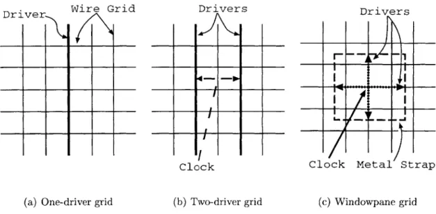
The tour de force of equipotential clocking was the first DEC Alpha chip [17] (Fig. 2-1(a)). In that design, a single, segmented buffer placed lengthwise in the center of the die drives a grid made using two upper metal layers (i.e., the thickest metal available, to lower T). The worst-case time difference between clock arrivals
was 200 picoseconds, and this was sufficient for a 200 MHz clock.
The next two versions, the 300 MHz Alpha and its strikingly similar 433 MHz cousin, [18, 19] both used two drivers for the entire grid (Fig. 2-1(b)). Why? With higher clock speeds, the RC delay from the center of the chip to the edges becomes significant; the two drivers effectively both drive halves of the chip, so the delays are shorter. The 600 MHz Alpha [2] (Fig. 2-1(c)) followed this trend: it has four top-level buffers, because with the higher clock speeds and wire delays, ever smaller sections of the chip can be modeled as equipotentials.
Wire Grid Drivers -o---Clock (b) Two-driver grid Driver
I I
Figure 2-1: Evolution of Alpha's grid based clock network. In all cases, large buffers drive a regular mesh of metal2 and metal3 wires.
2.1.2
H-Trees and Generalized Trees
If it were possible to lay out the clock net so that all points where the clock is used are equidistant from the clock driver, the wire delay would not cause skew. This idea led to H-trees (Fig. 2-2) [20, 21, 14].
By symmetry, the distance from the center of
the net (the root of the tree), to each of the ends
(leaves), is the same. Therefore, regardless of T,
signals should arrive at the leaves at the same time. The clock can then be distributed to a smaller (approximately equipotential) net around each leaf. The size of this equipotential region around each leaf shrinks as the depth of the tree increases, so deeper trees are needed for faster clock speeds.
The maximum clock frequency is limited by dispersion of pulses on the RC wires, so the basic
Leaf Leaf Leaf ...
Root
Leaf
Figure 2-2: Four level H-Tree. Paths from the center to the leaves are geometrically the same.
H-tree can be improved immediately by symmetrically inserting buffers along the
Drivers
I I
I I
-- -- ---
----Clock Metal Strap
(c) Windowpane grid
zlzI±Iz
branches to regenerate the signal [21, 22, 15, 14]. Clock trees are insensitive to global process and environmental variations; skew is still zero if the resistance of the wires is higher than expected, say, or if the input threshold to all the buffers changes. Of course, H-trees are affected by intra-die variations [23, 24]. Anything that causes similar paths on the different parts of the chip to have different delays (e.g., local line width variations, temperature gradients, varying threshold voltages, etc.) causes skew.
H-trees are most useful when clocking regular arrays, because the leaves form a regular grid. What can be done if the clock loading is not so geometrically regular? The vital feature of H-trees is that the distance from the root to all the leaves is the same. Finding a balanced tree for an arbitrary set of points is known as the
zero-skew tree problem. In general, finding a zero-zero-skew tree with minimum total length
is exceptionally hard; however, a number of heuristic algorithms have been proposed
[25, 26, 27, 28, 29]. Closely related to the zero-skew problem is the bounded skew tree
problem, where a small amount of path difference is allowed to help minimize the total wire length, and therefore minimize area and power dissipation [30].
All of these tree approaches are bottom-up
algorithms that start by connecting groups of nodes into a tree and then merging trees until Leaves only one net remains. They are distinguished
by exactly how they merge trees, behavior in
pathological cases, how the number of compu-Root
tations scales with the number of clock loads, Figure 2-3: Zero-skew balanced tree how they route around obstructions, etc. The result is essentially the same, however: they all produce an irregular clock tree that ties together a specified set of clock loads such that the distance from the root to the leaves is approximately equal (Fig. 2-3). Most modern processors use some version of such trees to distribute the clock [31, 32, 33, 34]. Those that do not use explicit trees still simulate and balance path delays from the clock source to all the loads, so act essentially as generalized clock trees. There the
Global Clock
Delay Delay-_
-Compare+-Figure 2-4: Digital active deskewing
matching is generally less precise, because the delay to the leaves, while nominally identical, is composed of the delays of a variable number of gates and length of wire, so even global variations in a particular parameter may cause skew.
2.1.3
Active Skew Management
One approach to measure and cancel out static skew involves splitting the H-tree into two halves, measuring the relative offset between the two, and applying the appropriate delay, as shown in Fig. 2-4 [35]. In this structure, the delays and control
signals are digital; this adds a measure of noise immunity, but increases the overhead power and area. Further, the model does not scale well - there is explicit digital control to guarantee that the delays do not both continue to increase. Splitting the tree into more sections allows finer adjustment, but the control overhead increases rapidly as well.
2.2
Previous Work: Variations
Because the goal of a clock network is to distribute an identical signal to multiple locations, device and interconnect matching is important. Environmental variables, such as supply voltage, switching activity and temperature depend on the design of
the chip, and hence are under the control of the designer. Conversely, processing variables, including film thickness, lateral lengths, resistivity, etc., are defined by the manufacturing process, and can be treated as imposed constraints [43]. This section describes some of the approaches to modeling the constraints and their effects on circuits.
2.2.1
Layout-Dependent Processing Variations
Some manufacturing process steps, most notably etching, chemical-mechanical pol-ishing (CMP) and lithography, are influenced by topography on a chip. This layout-depending processing causes systematic device and interconnect variations [43, 44, 45]. Modeling this variation falls into the realm of statistical metrology; see [46] for a re-view. This systematic variation need not limit clock performance, however. Design rules are evolving to ensure layout pattern uniformity. For some effects, it may be feasible to add a spatially-varying fabrication mask offset, just as masks are made
by adjusting the drawn layout to compensate for lithography and etching biases.
As a last resort, clock performance can be measured and systematic offsets can be compensated in the design.
2.2.2
Wafer-Scale and Random Physical Variations
Unlike systematic skew, skew caused by random physical variations is unavoidable. For example, a dominant source of device mismatch over small areas is V variation due to stochastic distribution of dopants; variation depends only on channel area [47, 45, 48, 49]. Wafer-scale non-uniformity, while not truly random, varies from chip to chip. For example, deposited thin films often have a radially-symmetric thickness profile across a wafer. This results in slants in parameter properties across chips that depend on position of the chip within a wafer, and hence cannot be compensated on
Voltage
Vth max
Vth min- -
--Time
tO t1 t2 t3
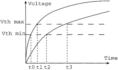
Figure 2-5: Clock skew caused by finite signal rise time. t1 - to and t3 - t2 is skew
due to variable buffer threshold voltages. t3 - ti and t2 - to is due to variable rise
time. t3 - to shows the worst case combined effect.
2.2.3
Circuit Implications of Mismatch
Processing mismatch translates directly into loss of clock performance. For example, variations in saturation current or buffer thresholds can both lead to variable clock arrival times, as shown in Fig. 2-5 [21, 20]. Exact numbers are not easily available, but one may assume that there could be 10% dynamic variation in VDD across a chip (which affects the threshold and drive current) and another 5% variation in IDSS
between two distant, though nominally matched, buffers. That leads to an expected clock skew of 2.5% of the total clock cycle from a single pair of gates! In the current regime, where the clock skew budget is approximately 10% of the clock period, this is quite substantial [22, 50, 51]. Attempts to increase the maximum clock speed by increasing pipelining along an H-tree exacerbate this effect [52].
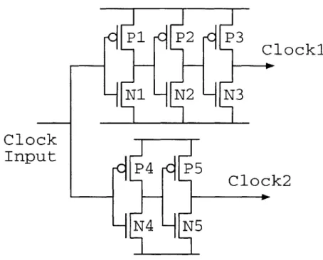
Because random variations cause substantial skew, there have been a number of attempts to minimize mismatches at the circuit level. For example, it was noticed that due to poor matching between nfets and pfets, signal paths which do not match the nfets and pfets separately may add skew unnecessarily [53]. The canonical example is shown in Fig. 2-6. On a rising input clock edge, gates N1, P2 and N3 are turned on in the top chain and N4 and P5 in the bottom chain. Because nfets may be expected to track nfets better than pfets, and vice versa, the lowest skew is achieved by sizing
P1 P2 P3
Clocki
N1
N2
N3
Clock
Input
I n p u t
4
P 5
C l o c k 2
N4 N5Figure 2-6: Independent balancing of NFETs and PFETS
the transistors so that dN1 + dN3 = dN4 and dP2 = dP5 where dN1 is the delay
due to transistor N1, etc. The general observation is that matching is best between similar components. One cannot expect wire delays to match gate delays over all process corners, for example.
Clock designers have also started to pay attention to wisdom from analog design: matching is best between similar elements, and matching between identical elements is improved by making them larger. For example, matching wire delays to gate delays is likely to lead to random skew. And when matching delays through a clock tree, at some times fast paths need to be slowed down. There are two straightforward ways to accomplish this: make the wires longer or make them wider. Which is better? Wider wires are preferable because of the diminished influence of edge effects [50, 54, 55].
Consideration of random variations is becoming increasingly important in clock designs. The solutions tend to be ad hoc, and there has been little work on how well physically separated components may be expected to match. And most clock trees are still designed to achieve minimal nominal skew without consideration for how random variations will affect performance.
2.2.4
Abstract Variation Models
At the other end of the extreme from the ad hoc physical models are the abstract models for skew [15, 56, 42, 57]. The assumption in these models is that skew is caused
by uncorrelated, random variations in the clock distribution network. Unfortunately,
because they are so far removed from implementation, generic statistical models give somewhat misleading results, for several reasons.
The first is that they are too optimistic about statistical independence of vari-ations. For example, gates that are near each other are likely to match each other more so than gates that are physically separated. This means that the sum of the skews caused by gates in any signal path will have higher variance than would the sum of skews caused by the same number of gates randomly selected from the chip. Also, as has been pointed out, not all variations have the same weight in the final skew: clock trees, for example, are much more sensitive to differences at the root of the tree than at the leaves [56].
Ironically, the second weakness is that general statistical models can be too
pes-simistic as well. For example, an analysis of pulse width down a long line of buffers
suggests that the pulse-width follows a random walk [57]. Thus, it is argued, the pulse might disappear entirely unless the clock period is sufficiently long. In fact, it is not particularly hard to add feedback to ensure a 50% duty cycle, which effectively limits the random walk. In this case and some others, circuit tricks can overcome apparent stochastic barriers [15].
Fundamentally, the very generality that makes sweeping statistical statements interesting is their weakness because such bounds do not take into account circuit or architectural changes that affect network performance. Although they may place bounds on clock performance, they are necessarily qualitative, and can neither suggest circuit improvements nor take them into account.
2.3
Categories of Mismatch
All on-chip clock networks rely on device parameter matching. This is a crucial
difference between logic critical paths and clock networks: variation in critical path delay can be overcome by speeding up the critical path so that the worst-case delay meets timing constraints [58]. Time-dependency logic delay can be included directly in the worst-case timing estimates: maximum delay is constrained by Eq. 1.3 and minimum delay by Eq. 1.4. In contrast, because the clock network itself establishes the timing, both too-slow and too fast clocks must be avoided. Physical variations are often separated into separated into local and global contributions [59]. For the purposes of clock distribution, time-varying mismatch must be considered explicitly as jitter (and, if uncorrelated spatially, as contributing to skew).1
Integrated circuit fabrication processes generally result in wafer-scale gradients in line width (both metal and polysilicon), thin film thickness (metal wires, gate oxide, interlayer dielectric) and doping concentration [43]. Manufacturing gradients have been cited to explain distance-dependent mismatch in transistors [60]. These variations significantly affect device and interconnect performance. In minimum-size inverters, for example, Leff variation can lead to 9% delay mismatch [61] between chips; in a different process 37% variation of ring oscillator speed was reported within single dies [62]. Clocks depend on matching rather than absolute delays, and are therefore insensitive to truly global parameter variations. We also make the optimistic assumptions thatall systematic variations are compensated. This could be achieved via modeling (i.e., statistical metrology), or simply testing finished chips if multiple silicon revisions are to be made.
However, because clock networks span an entire chip, wafer-scale gradients are noticeable. It is generally accepted that global effects can be ignored for distances smaller than 100pm, but are noticeable for distances larger than 1mm [47, 60]. Global environmental variations, specifically in temperature and DC supply voltage variation,
'There is a subtle asymmetry between temporal variation in logic and clock. Slack in Eq. 1.4 can not be exploited to decrease clock cycle time, while any decrease in clock uncertainty directly lowers the minimum clock period. For this reason, temporal variations of the clock are analyzed explicitly.
Figure 2-7: Example H-tree
Segment 1 2 3 4 5 6 7 Average
Xi 0.1 0.3 0.5 0.5 0.5 0.4 0.25 .36
Table 2.1: Contributions to skew for an H-tree
are imposed by design rather than fabrication, but are otherwise similar in effect. Temperature affects resistivity of the metal, channel mobility, and threshold voltages, and supply voltage affects saturation currents and hence gate delay [63].
The distance between most nominally matched components of a clock distribution network is comparable to chip size, which is typically 1cm or larger. Fig. 2-7 shows an example H-tree, and the distances xi, normalized to chip size, between nominally matched wire segments are tabulated in Table 2.1. Most of the distances are com-parable to the size of a chip; hence, we may expect that the wafer-scale variations are dominant and consider inter-chip mismatch data. Still, this brings up a messy modeling issue.
Delay along a clock wire is a sum of small delays. The delay of each buffer-x7 x5 x6 x4 X1 x3 x2
wire-buffer segment contributes a small random component. If the segments are strictly independent (e.g., uncorrelated threshold voltage variations), the variance along the wire is the sum of individual variances, so the standard deviation of the resulting offset increases as the square root of the length of the wire. Another model is that the mismatch is due to a gradient of delays across a chip (perhaps from thin-film deposition). Because the linear gradient is summed, the mismatch rises with the
square of the wire length. Finally, if the perturbations are each fixed-size or uniformly
distributed (e.g., a higher supply voltage for a section of the chip) , the worst-case offset increases linearly with wire length.
Because gradients dominate over relatively long distances, it would probably be most accurate to model short nearby wires with independent segments, long distant wires in terms of gradients, and intermediate wires linearly. However, that obfuscates the analysis unnecessarily; the key point is that short near wires match better than long distant wires. For the sake of analysis, we will assume that uncertainty scales linearly with delay with a mismatch coefficient a, as p(x) - p(0) . ap(O).
This argument can be extended to say that the variability in delay along a path scales linearly with the delay along the path; that is, that there is a fixed percentage error in on-chip path delay. We will use this assumption, although there is an impor-tant caveat: a depends on the construction of the path. A Ins delay with a = 0.11 gives more skew (110ps) than a 1.lns delay with a = 0.09 (99ps). For this reason the
classic line-driver optimization may give suboptimal results if wire mismatch is not the same as buffer mismatch. However, for the optimal combination, delay variability will scale linearly with delay.
Of course, matching is not perfect for adjacent wires or devices either. Strong
sensitivity of threshold voltage and saturation current on L at short channels also limits matching for minimum-size devices; typically saturation current has a 3% mis-match for minimum devices, and mis-matching down to 1% is straightforward in larger devices. Local mismatch is an important limit for phase detector offset in PLL and DLL systems.
clock lines and signal-dependent capacitance. Careful layout can minimize the ca-pacitance between signal lines likely to switch near clock edges and clock wires, but signal coupling is still important because it can be a significant source of jitter. We will assume that up to 5% of the capacitance of any wire may transition during the
time a clock edge propagates.
Temperature changes on a chip are generally many orders of magnitude slower than the clock speed, and are therefore reasonably treated as static gradients. On the other hand, supply voltage can change within a single clock cycle in response to changing load current. For this reason, temporal correlation is important when matching elements that depend on supply voltage. An example where this is signifi-cant is described in Section 2.4.4.
2.4
Clock Architecture Comparison
While a number of authors have considered the impact of variations on clock perfor-mance, most assume tree distribution [52, 41, 63]. This section establishes a common metric and compares several clock architectures.
2.4.1
Clock metric
The three categories of mismatches listed above cover what is needed for a first-order comparison of clock networks. For normalization, each is scaled to distribute a 1 GHz clock to a total of 200pF load capacitance over a 2cm chip in a standard 0.25pm
CMOS process. A clock wire in a TSMC 0.25pm CMOS process would be 1pm wide,
have a resistance of about 0.07Q/pm, and a capacitance of .lfF/pm.
It would be convenient to choose a single parameter to characterize clock networks. As discussed earlier, skew and jitter are in general functions of both position and time. It is appropriate to consider the worst case clock uncertainty over time, but meaningless to look at worst case across a chip: in all practical cases a signal that takes longer than a clock cycle to propagate would be pipelined, and hence re-clocked. Hence, clock uncertainty between points on a chip further apart than one clock cycle is
.05C
Figure 2-8: Schematic model of capacitive coupling
irrelevant. For this reason, the metric for clock quality will be taken to be worst-case clock mismatch over a distance corresponding to signal propagation distance during one half of a clock cycle.
2.4.2
Tree
Propagation delay along an H-tree can be split into delay from the root to the leaves, and delay from the leaves to a sub-block or tile. Delays to loads from a leaf are generally not matched, so the entire delay in a sub-block adds directly to total skew; this is sometimes called internal clock skew [14, 63]. The point of an H-tree, however, is to match delays from the root to the leaves, so those delays are nominally matched, and only variations contribute to skew. Consider a 8-level H-tree (i.e., one with
28 = 256 leaves). Assuming equal-sized buffers along the tree, these buffers would be
placed at intervals of perhaps 2mm, for a total of 10 segments.
Delay along the tree in this example is simulated to be 0.86ns. Assuming a = 0.1,
skew caused by gradient mismatch is 0.86ns x 0.1 = 86ps. Internal skew (Si) is no
larger than 0.07Q x 625pm x 0.2pF ~ 9ps.
Capacitive coupling adds a time-varying offset. Fig. 2-8 shows the schematic model used to test the effect of capacitive coupling. The effect may be estimated by adjusting the effective line capacitance for the Miller-multiplied coupling capacitance. In the current example, the line capacitance is 200fF, the output capacitance of the driving buffer is 34fF, and the input capacitance to the receiving buffer is 77fF. A signal making a transition in the same direction as the clock lowers the effective wire
capacitance by 5% (given the assumptions above), so the delay should decrease by
.05x200 ; 3%. Conversely, a signal transitioning in the opposite direction will slow
200+ 111
down the clock by the same 3%, so the total would be up to 6% variation. (Simulation indicates the total variation is 5%). This component of uncertainty - skew if the interference recurs on every clock cycle, jitter if it is inconsistent - also scales with the total delay along the tree, and so adds a worst-case 45ps to clock uncertainty.
To sum up, a clock distributed by a tree as described above will have skew of 140 picoseconds, or 14% of the clock cycle; this is in line with industrial results given the speed and assumptions about the process.
Generalization
We can generalize from this example to other trees. Fig. 2-9(a) shows how the two components of skew change with the depth of the tree, n. (The tree of this example had n = 8.) As argued above, both mismatch and coupling cause skew proportional
to wire length L from root to leaves of the tree; in units of chip size, L = 1 - (1/2)n/2. Internal skew scales inversely with the area2 of the resulting patch, so Si oc 2-.
The other key parameter is power. Power scales linearly with switched capaci-tance, so the clock distribution power (excluding the load) scales as 2n/2. Fig. 2-9(b) combines the results into a plot of the fundamental clock network tradeoff between power and performance.
Scaling
Note, however, that a clock tree does not scale well with process technology. As chip dimensions shrink, wire delay (T) is, at best, constant. Total chip size is also
nearly constant. However, clock speeds increase as the gate delay decreases. Delay along the clock net also speeds up, but not by the same factor. Along an optimally buffered line, the ratio of gate delay (d) to T is constant, so as d falls, the distance between buffers decreases. Wire delay is proportional to the square of the wire length
2Strictly speaking, it scales with length squared, but that is equivalent to area for non-pathological
10 4 100
-x- area-scaled skew 0
-&- length-scaled skew -2
U -- total 0 2U S10 2 10 - -co 0 C N 10 1s -2 10 E 10 0 0 0 10 10 10 102 10 10
depth of tree skew, ps
(a) Skew components in a tree vs. tree depth (b) Power vs. skew for a clock tree Figure 2-9: Clock tree tradeoffs
between buffers (1). Hence 1 cx Vd. The total number of segments is proportional to
1/1, so the total delay along a tree is proportional to d/Vdi = v
/d.
Since the clock speed is directly proportional to d, skew as a fraction of the clock period will grow as 1/v d as gate delay falls. In other words, without a dramatic redesign or process improvements, a 4GHz clock tree would have unpredictable clock skew of 30% of a clock period, and a 16GHz clock would have to budget over half of the clock period for skew and jitter margin.Note that as clock speed increases, signal delay across a chip exceeds a single clock cycle. In the example above, a 2cm-long wire has a delay of 0.86ns with 1GHz clocks. Scaling to 4GHz, the same wire (with optimal buffering) will have a delay of approximately 0.43ns, compared to a clock period of 0.25ns. Given the metric defined in Section 2.4.1, therefore, there is no reason to minimize global skew at all. In a tree, however, the worst-case skew occurs between nearest neighbors, so tree distribution cannot take advantage of the relaxed global constraints. This is the fundamental reason why trees become less attractive at high clock speeds.
Global Clock
Figure 2-10: Grid distribution block schematic
2.4.3
Grid
A pure grid network would have a single, central driver for the entire chip and a mesh
of clock wires. Skew would be simply the wire delay across the chip, just as it is the wire delay in a patch for each leaf of a tree. In the limiting case, a clock plane with a central driver would give skew of .07Q/pm x .lf F/um x (104pm)2 = 0.7ns.3 Clearly,
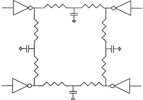
a single driver will not give adequate performance, so modern grids are H-tree-grid hybrids: a short H-tree distributes clock to a few (4 or 16, for example) buffers around a chip, and those buffers drive a clock grid in parallel, as shown in Fig. 2-10. The final patches are larger than those typical of trees, but the grid helps eliminate skew caused by the tree distribution by shorting together outputs of multiple buffers.
Take as an example system a 4 level (24 = 16 node) clock tree where the final buffers drive a global grid. Following the example of the previous section, such a tree would have 7 2mm-long segments and an expected clock uncertainty of 70ps. Delay across each region, assuming a lumped model with minimum-width wires, would give a skew of 2.5mm x 70Q/mm x 6.25pF ~ 1ns. Because this skew is dominated by wire resistance and load capacitance, it can be reduced by increasing the width of the wires at the cost of increased power. At the point where the capacitance of the wires
3Scaling this value down to the size of the first Alpha gives skew ~ 200ps, which was reported
Figure 2-11: Model circuit for shorted grid drivers.
equals the load capacitance there is one clock wire every 200pm, and the expected wire skew is 89ps, (85ps simulated).
Furthermore, shorting the buffers together helps drive down some of the uncer-tainty at the cost of increased short-circuit power during switching and somewhat slower edge rates. A simple circuit model for a grid driven from multiple points is shown in Fig. 2-11. Simulations with an 70 picosecond skew on buffer inputs show a total skew of 145ps, of which 55ps is due to the input skew. It is possible to keep driving this lower by increasing wire width; however, the benefits of wider wires get incrementally smaller as the wire capacitance comes to dominate the total. Doubling the wire width again, for example, lowers total skew to 110ps, of which 34ps is due to the input.
The drawback, of course, is the power dissipation. The extra wiring needed to get 110ps skew down added 25pF of capacitance per buffer, while the clock load per buffer is only 12.5pf. Still, grid distribution is used because much of the skew is predictable and, unlike with H-trees, the clock design is largely independent of floorplanning.
10 0 00 o 0 75 10 0 101 N S10' 0 CL10-3 101 102 103 skew, ps
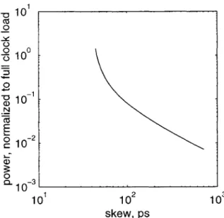
Figure 2-12: Power vs. skew for a grid.
Generalization
The primary parameter for a gridded clock is the capacitance of the grid (C); that
sets both the power dissipation (P oc C) and the wire skew. Si is proportional to
1 + CL/C where CL is the load capacitance and C the grid capacitance. Mismatch-induced skew is shorted out by lower-resistance wires, so that component of skew falls as 1/CL. A plot of simulated power dissipation vs. skew, corresponding to Fig. 2-9(b) is shown in Fig. 2-12.
Scaling
Grid distributions depend only on wire delays. As mentioned above, wire delays tend not to improve with process technology scaling. As the skew budget decreases with rising clock speed, a grid clock must either increase capacitance or subdivide the chip further with a deeper initial clock tree. In the example above, the initial tree itself does not add significant power, so an obvious scaling strategy would be to simply
make larger trees to minimize Si.
As long as delay variations in the initial tree are comparable to rise time, deeper
trees and smaller Si will improve performance. However, rise time scales linearly with d, so by the same reasoning as as applied to the tree scaling arguments, skew
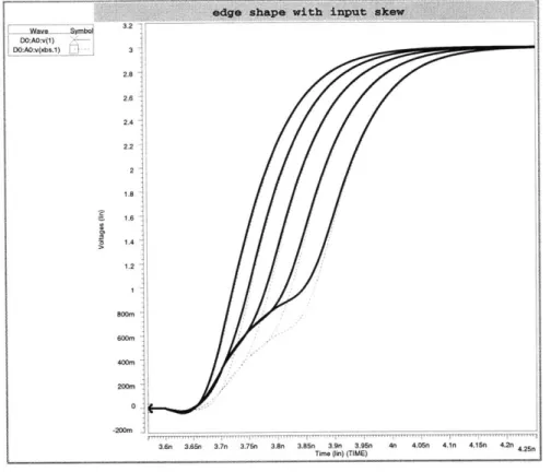
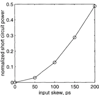
as a fraction of rise time will increase with 1/vd as gate delay falls. When the tree skew exceeds rise time short circuit power dissipation increases rapidly, and the clock edges begin to show an unacceptable kink. Fig. 2-13 shows simulated edge shapes with increasing input skew for a grid driven from a 4-level tree with skews from 0 to 200ps, and Fig. 2-14 shows the corresponding short circuit power dissipation.
DCWAO:v) y-D0: V(xbs1) -3.2 3 2.8 2.6 -2.4 2.2 1.8 1.6 1.4 -1.2 1T 800m -400m 200m 0 -20Cm -3.6n 3.65n 3.7n 3.75n 3.8n 3.85n 3.9n 3.95n
Time (fin) (TIME) 4n 4.05n 4.1n 4.16n 4.2n 4.25n
Figure 2-13: Simulated edge in a grid with skew to the drivers.
2.4.4
Active Feedback
As is evident from the sections above, an increasing share of skew comes from the initial long-distance distribution of a clock to relatively small loads. A delay-locked loop (DLL) could be adapted to measure and cancel out wire variations. One possible implementation is shown in Fig. 2-15, where a DLL is used to implement a single wire with low effective delay. The intuition is that the delays are adjusted symmetrically until the round trip time from the source to the load and back is a known multiple of a clock period; (in line with the examples so far, assume the round trip time is
0.5 0 0.4-> 0.3 0 c _00.2 a) N E0.1 0 0 50 100 150 200 input skew, ps
Figure 2-14: Short circuit power in a grid vs. input tree skew.
Source D/2 W1 b2 w2 bw13 w3 b4
Load
b8 w7 b7 w6 b6< w5 b5
Figure 2-15: Low-skew wire with DLL
2ns, which is 2 clock periods). Then by symmetry, the signal arrives at the load with a 1 period clock delay, which means it has effectively 0 delay for clock signals. Unfortunately, this intuition is misleading.
Despite the apparent symmetry, there is little reason for the forward path to match the reverse path in this connection for two main reasons. First, the nominally
matched buffers are physically separated. In Fig. 2-15, b1 should match b7, although
it would be physically near b8. b, isn't as far away from its matched pair as it might be
in a tree, but it will still typically be millimeters away. Second, there is no temporal
correlation. The clock signal passes w, at a different time than it passes w7, so
any time-dependent variations, including those due to power supply and capacitive
coupling, do not match. Taking the results from Section 2.4.2, the effective skew for a