HAL Id: hal-01651965
https://hal.archives-ouvertes.fr/hal-01651965
Submitted on 25 Jan 2021
HAL is a multi-disciplinary open access
archive for the deposit and dissemination of sci-entific research documents, whether they are pub-lished or not. The documents may come from teaching and research institutions in France or abroad, or from public or private research centers.
L’archive ouverte pluridisciplinaire HAL, est destinée au dépôt et à la diffusion de documents scientifiques de niveau recherche, publiés ou non, émanant des établissements d’enseignement et de recherche français ou étrangers, des laboratoires publics ou privés.
Structural and mechanical characterization of hybrid
metallic-inorganic nanosprings
Sabrina Habtoun, Saïd Houmadi, Benjamin Reig, Emilie Pouget, Dmytro
Dedovets, Marie-Hélène Delville, Reiko Oda, Fuccio Cristiano, Christian
Bergaud
To cite this version:
Sabrina Habtoun, Saïd Houmadi, Benjamin Reig, Emilie Pouget, Dmytro Dedovets, et al.. Structural and mechanical characterization of hybrid metallic-inorganic nanosprings. Materials Research Express, IOP Publishing Ltd, 2017, 4 (10), �10.1088/2053-1591/aa8e1a�. �hal-01651965�
Materials Research Express
PAPER
Structural and mechanical characterization of
hybrid metallic-inorganic nanosprings
To cite this article: Sabrina Habtoun et al 2017 Mater. Res. Express 4 105023
View the article online for updates and enhancements.
Related content
Suspended tungsten-based nanowires with enhanced mechanical properties grown by focused ion beam induced deposition
Rosa Córdoba, Matteo Lorenzoni, Javier Pablo-Navarro et al.
-Complex tribomechanical characterization of ZnO nanowires: nanomanipulations supported by FEM simulations
Sergei Vlassov, Boris Polyakov, Sven Oras et al.
-Material characterisation of nanowires with intrinsic stress
S Mills, J E Sader and J J Boland
© 2017 IOP Publishing Ltd
1. Introduction
Nanosprings (NS), also known as nanohelices or nanocoils, are 1D-nanostructures which exhibit a helical morphology. These structures have triggered great interest over the past decade, as their size and their geometry give them striking properties such as flexibility, periodicity, chirality and high surface-to-volume ratio [1–3]. Therefore, they have been integrated into functional devices in the field of photonics [4, 5], electromagnetism [6,
7], mechanical actuators [8, 9] and chemical sensors [10, 11].
Their fabrication can either be carried out by top-down or bottom-up methods, such as oblique angle deposi-tion [12], catalyzed CVD [13, 14], bilayers of pre-stressed films [15], self-assembly in solution [16]. These meth-ods allow the synthesis of NS of various materials [17]; however, they often suffer from a cost or a yield problem. Even fewer examples of metallic NS are found in literature made of palladium [18] or copper [19], except for the case of vertical mats of NS [20].
The NS used in this work are synthesized by an already published bottom-up method [21, 22] which allows a high-yield production of silica nanohelices in solution. Nonetheless, the lack of conductive properties limits their usability in functional devices. A first step towards this goal in this study was to obtain metallic helical nano-structures whose mechanical properties are suitable for designing electromechanical sensors and actuators.
We describe here a lithography-free method to both clamp and metallize isolated suspended NS. Using a focused ion beam (FIB), we carried out electron-beam induced deposition (EBID) for an easy prototyping, ena-bling NS characterization without the need for lithographic processing. Our goal was to investigate the nature, structure and geometry of the deposited metallic layer on the surface of the NS. Then using an atomic force microscope (AFM), we carried out a mechanical characterization of the obtained hybrid metallic-inorganic NS.
S Habtoun et al
105023
MRX
© 2017 IOP Publishing Ltd 4
Mater. Res. Express
MRX 2053-1591 10.1088/2053-1591/aa8e1a 10
1
8
Materials Research Express IOP
11
October
2017
Structural and mechanical characterization of hybrid
metallic-inorganic nanosprings
Sabrina Habtoun1, Said Houmadi1, Benjamin Reig1, Emilie Pouget2, Dmytro Dedovets2,3,
Marie-Hélène Delville3, Reiko Oda2, Fuccio Cristiano1 and Christian Bergaud1
1 LAAS-CNRS, Université de Toulouse, CNRS, 7 avenue du Colonel Roche, F-31031, Toulouse, France
2 Chimie et Biologie des Membranes et des Nanoobjets (CBMN), CNRS—Université Bordeaux—Bordeaux INP, UMR5248, Allée St Hilaire, Bat B14, 33607 Pessac, France
3 Institut de Chimie de la Matière Condensée de Bordeaux (ICMCB), CNRS-UPR9048, Université Bordeaux, 87 avenue du Dr A Schweitzer, 33608 Pessac, France
E-mail: bergaud@laas.fr
Keywords: atomic force spectroscopy, nanomechanics, nanostructure, nanohelix, nanospring, EBID, FIB
Supplementary material for this article is available online
Abstract
Silica nanosprings (NS) are fabricated by a sol–gel deposition of silica precursors onto a template made of self-assembled organic chiral nanostructures. They are deposited and assembled on microstructured silicon substrates, and then metallized and clamped in a single lithography-free step using a focused ion beam (FIB). The resulting suspended hybrid metallic/inorganic NS are then characterized with high-resolution transmission electron microscopy (HRTEM) and scanning TEM/ energy-dispersive X-ray spectroscopy (STEM/EDX), showing the atomic structure of the metallic layer. Three-point bending tests are also carried out using an atomic force microscope (AFM) and supported by finite element method (FEM) simulation with COMSOL Multiphysics allowing the characterization of the mechanical behavior and the estimation of the stiffness of the resulting NS. The information obtained on the structural and mechanical properties of the NS is discussed for future nano-electro-mechanical system (NEMS) applications.
PAPER 2017 RECEIVED 7 August 2017 REVISED 20 September 2017
ACCEPTED FOR PUBLICATION
21 September 2017
PUBLISHED
16 October 2017
https://doi.org/10.1088/2053-1591/aa8e1a Mater. Res. Express 4 (2017) 105023
S Habtoun et al
Structural, chemical and mechanical properties were investigated, in order to assess whether these nanostruc-tures could be integrated in nano-electro-mechanical systems (NEMS).
2. Experimental section
2.1. Silica NS
Silica NS were synthesized using a process thoroughly detailed in previous articles [21, 22]. To sum up, a two-step synthesis process in solution was performed. First, the association of cationic gemini surfactants of chemical formula C2H4-1,2-((CH3)2 N+C16H33)2, with chiral counter-ions, tartrate, creates a gel of helical organic
nanostructures. The shape of the nanostructures (helical pitch, diameter and length) can be controlled by various parameters such as molecular composition or fiber formation kinetics. The control of the experimental conditions such as temperature, pH and aging of the gel allows a tuning of the shape of the nanostructures, which can be obtained as tubules, twisted ribbons or the NS used in the present work. The resulting NS are suspended in a 1:1 ethanol/isopropanol solution. In a second step, these are used as templates for the sol–gel deposition of silica, using tetraethyl orthosilicate (TEOS) as a precursor. The templates are then removed by washing with ethanol and propanol, resulting in silica NS, with an outside diameter of 30 nm and a length of the order of a few micrometers after redispersion in ethanol/propanol by ultrasonication [22]. Figure 1(a) displays a SEM picture of the resulting nanostructures deposited on silicon.
2.2. Oriented assembly and metallization of the silica NS
The substrates used in the present work were 4-inch silicon wafers, which were patterned by photolithography using a Canon stepper and AZ ECI photoresist. Trenches were etched by KOH anisotropic wet etching or deep reactive ion etching (DRIE), their widths ranging from 0.5 to 1.5 µm. A drop of a suspension of NS in a 1:1
isopropanol/ethanol was deposited onto a silicon wafer etched with micron-sized trenches which were made hydrophilic by O2 plasma. 10 µl of the solution of NS were injected under a microscope coverslip. The resulting
hydrodynamic flux and evaporation resulted in the alignment of the NS over the silicon trenches [23]. The microscope coverslip was then removed and the sample was dried under ambient conditions. The statistical analysis of the orientation of the NS with respect to the induced capillary forces showed that 45% of the NS are oriented in the direction corresponding to the induced hydrodynamic flow. This assembly was performed in such a way so as to position the nanostructures perpendicularly to the trenches for mechanical characterization. Individual NS suspended over trenches were located by SEM (supporting information figures S1–S3 (stacks.iop. org/MRX/4/105023/mmedia)).
We subsequently used a dual-beam focused ion beam scanning electron microscope (FIB-SEM) to deposit platinum in order to both clamp and metallize the NS in a single step. This instrument enables two kinds of deposition, one for each of the available beams: EBID, using the electronic beam of the SEM and ion-beam induced deposition (IBID), using gallium ions. The FIB used in this study was a Helios-FEI 600i equip-ment. The platinum was deposited using methylcyclopentadienyl(trimethyl) platinum(IV) as a precursor. For EBID, dwelling time was 1 µs, with a beam at 25 kV and 43 pA, and a working distance of 4.2 mm. The
thickness of the metallic films was controlled by the deposition time and the overlap of the spot. For IBID, the deposition parameters were a dwelling time of 1 µs, with a beam of 30 kV and 1.1 pA, at a working distance
of 4.2 mm.
Both approaches allow an easy prototyping of different thicknesses and geometries of the deposited metallic layer. The drawbacks are first the purity of the film: hydrocarbons present in the vacuum chamber are deposited at the same time, adding carbon to the deposited layer. Many teams tried to solve this issue by annealing the sam-ples under an atmosphere of O2 [24], H2 [25, 26] or under vacuum [27]. The second shortcoming is the parasitic
deposition around the patterning caused by (i) the beam being non-punctual and (ii) a redepositing process caused by the subsequent observations using the electron beam. In the present study, to avoid a parasitic plati-num redepositing process, particular care was paid to wait for the chamber pressure to stabilize between each deposition and preliminary observations were carried out far from the area of interest.
2.2.1. IBID
In the case of IBID, two kinds of depositions were carried out: a thin one (which minimized the alteration of the helical geometry) and a thick one, which modified the NS into a nanoscale cylinder. The measured thicknesses ranged from 5 to 100 nm. Indeed, the drawbacks of IBID are first the difficulty to get a thin reproducible film and second, the great damage induced to the delicate surface of the NS, due to the high energy of the ions: it takes only a few passages of the beam to etch out the structures. For these reasons, IBID was not used for Pt deposition on the NS in this study. Only the preparation of the TEM cross-section lamellas was performed using IBID to obtain a thick Pt layer.
3
S Habtoun et al
2.2.2. EBID
EBID deposition uses the electronic beam. It is much slower than IBID but more controllable. The helical configuration of the NS was preserved in each case. The deposited thicknesses ranged from 3 to 20 nm. However, the purity of the deposited films is lower than those made by IBID, due to a higher carbon content.
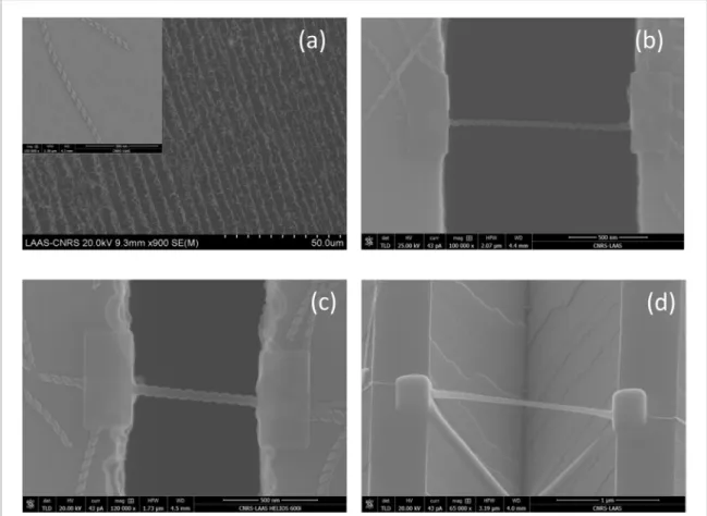
Figure 1(a) shows a SEM image of silica NS deposited on a silicon substrate using oriented capillary assembly with a closer view on individual ones in the inset. Figures 1(b)–(d) shows the morphology of the resulting hybrid metallic-inorganic NS obtained using the two modes of coating: thin coating using EBID (figure 1(b)), EBID thick coating using EBID (figure 1(c)), and thick coating using IBID (figure 1(d)). The helices are both clamped and suspended, which allows an easy mechanical characterization with an AFM.
3. Results and discussion
3.1. HRTEM and STEM/EDX characterization
HRTEM and STEM/EDX were used in order to characterize the morphological and chemical structure of the deposited metallic layer. The HRTEM and STEM/EDX observations were performed on a JEOL 2100F FEG electron microscope installed in the Raimond Castaing microcharacterization Platform of Toulouse. The sections were prepared by first protecting the spot of interest with an EBID carbon deposition to fill the trench and cover the NS. The sample was then etched to a thin section of about 100 nm by using a Gallium ion beam.
Observations were performed on NS metallized using EBID only, as the layers were thinner than those obtained with IBID and the structures retained their helical geometry. The goal of these observations was to check whether the platinum film was homogeneously deposited around either side of the NS despite the fact that they were irradiated from the upper surface by the electron beam during EBID. The determination of the radial morphology of the deposited layer is impossible using SEM or AFM while its imaging perpendicularly to its axis is of greatest interest to characterize the thickness of the metallic layer and the NS chemical distribution, espe-cially if one wants to properly model their mechanical and electromechanical behavior.
We performed two kinds of observations: one direct ‘plan-view’ observation of metallized NS dispersed on a TEM carbon grid and a ‘cross-section’ TEM analysis where the NS were observed across their circular section. To prepare TEM cross sections, samples of suspended metallized NS above silicon trenches were embedded in
Figure 1. (a) SEM image of silica NS deposited on a silicon substrate using oriented capillary assembly with a closer view on
individual ones in the inset. SEM images showing the morphologies of suspended NS after metallization and clamping by FIB. (b) EBID thin coating. (c) EBID thick coating. (d) IBID thick coating.
S Habtoun et al
a layer of carbon deposited by EBID and were subsequently covered by a thick Pt layer deposited by IBID. The obtained samples were thinned down to a thickness of 100 nm and then cut from the silicon substrate using FIB etching. The resulting cross-section is then held onto a TEM grid using a micromanipulator (see supporting information figure S4).
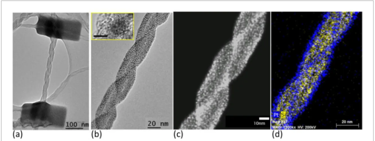
As can be seen from the HRTEM and STEM/EDX observations displayed in figure 2, the metallized NS are covered with small crystalline nanoparticles of less than ~2 nm in diameter (figures 2(a) and (b)). No such particles have been seen in the NS prior to metallization suggesting that they consist of Pt. The observed nano-particle size is in agreement with values published in previous reports on Pt nanostructures grown by EBID [24,
28, 29]. The images taken in STEM/HAADF mode (figure 2(c)) show a bright contrast originating from the nanoparticles, indicating that they are composed of atoms with heavier atomic mass (Pt) compared to those con-tained in the silica NS (Si and O), in agreement with the previous observation. Indeed, the STEM/EDX chemical map (figure 2(d)) confirms that the observed nanoparticles are Pt precipitates. In addition, it appears that the Pt signal (blue in the figure) is detected on the whole surface of the NS, with a higher intensity on its periphery.
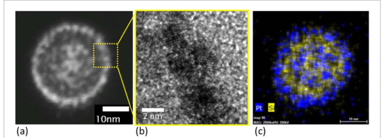
Finally, the analysis of the cross section of one of the metallized NS (figure 3), allowed us to confirm the pres-ence of a homogenous and symmetric metallic coating on both the outer and inner faces of the NS, as can be seen from the STEM/HAADF (a), HRTEM (b) and STEM/EDX map (c) displayed in figure 3. Additionally, from the HRTEM images, the thickness of the nanoribbon forming the metallized NS was also estimated to be around 7.5–8.0 nm compared to 2.5–3.0 nm for the NS prior to metallization (see supporting information figure S6).
As observed by HRTEM and STEM/EDX on cross-sections of metallized NS using EBID (figure 3), the depos-ited Pt is clearly present both outside and inside the SiO2 frame. To investigate the reason for this Pt distribution,
we used Casino, a software based on the Monte-Carlo method to simulate the interaction between an electronic beam and atoms [36]. With a beam energy of 25 keV as used in our experiments for EBID deposition and consid-ering 100 000 electrons interacting with a 10 nm-thick SiO2 surface during the simulation, more than 99% of the
incident electrons are transmitted across the SiO2 layer with no energy loss. Pt deposition using EBID at 25 keV is
therefore expected to occur both in the outer and inner faces of the NS in the presence of the reacting gas.
3.2. AFM Bending tests
3.2.1. Principle of the three-point bending tests
AFM measurements were performed on Bruker’s Dimension Icon. Tips were SCANASYST-Air, which stiffness is around 0.4 N/m, which is close to that of the investigated nanostructures. First, a calibration of the cantilever stiffness was carried out using a fitting with a thermomechanical noise model. The uncertainty on these measurements was of 20%. The vertical sensitivity of the photodetector was then calibrated by performing a force curve on the silicon substrate (considered to be infinitely stiff compared to the NS). The force–distance curves obtained had their baseline corrected to 0 N using Nanoscope Analysis and were then processed by a Scilab script to obtain the stiffnesses from the slopes of the linear portions of the curves.
AFM three-point bending tests are among the most frequently used methods for the characterization of 1D nanostructures [30–33]. In a previous work, we have already performed these tests on silica nanotubes formed
Figure 2. Plan-view TEM analysis. (a) HRTEM image of a NS metallized and clamped at both ends with Pt using EBID. (b)
Magnification of the HRTEM image of the metallized NS showing the presence of crystalline nanoparticles (see inset, scale bar: 2 nm). These nanoparticles are not seen in the as-grown NS (see supporting information figure S5), suggesting that they consist of Pt. (c) STEM image in high-angle annular dark field imaging mode (HAADF). The bright contrast originating from the nanoparticles indicates that they are composed of atoms with heavier atomic mass (Pt) compared to those contained in the silica NS (Si and O), in agreement with the previous observation. (d) STEM/EDX Pt signal (blue) is detected on the whole surface of the NS with a higher intensity on the periphery of the NS (the signal from the Si appears in yellow), confirming that the observed nanoparticles are Pt precipitates.
5
S Habtoun et al
from the same self-assembly process, albeit with different experimental conditions [21]. This allowed us to char-acterize the properties of the silica forming these structures, leading to the estimation of a Young Modulus of 74 ± 7 GPa, in good agreement with the bulk value [34]. In brief, two force–distance (F–d) curves are recorded: one on the nanostructure resting on the substrate, and one at the midpoint of the doubly-clamped suspended nanostructure as shown in figure 4. This setup enables to get rid of the influence of the cantilever deflection on the measurement and of a possible indentation of the NS by the AFM tip. In this way, it is possible to get the actual stiffness of the nanostructure.
From the linear part of each F–d curve, we have the general expression:
=
F kZ
(1) where F is the applied force, k the apparent stiffness and Z the deflection of the cantilever. In the linear regime,
k corresponds to the slope of the F–d curve. The slope obtained from the NS on the substrate gives the effective
stiffness kC of the AFM cantilever, while the slope S obtained at the midpoint from the suspended NS corresponds
to the contribution of kC and kNS, the stiffness of the NS.
This analysis yields this expression:
= +
S k k
1 1 1
C NS
(2) and thus we have:
= ⋅ − k S k k S. NS C C (3) A thorough calibration of the deflection sensitivity of the AFM and of the stiffness of the cantilever was carried out. This step enables a quantitative measurement of the forces applied to the NS. The stiffnesses k were calculated from the extension curves, less prone to the influence of adhesive effects than the retraction ones.
Figure 3. TEM images of the cross-section of a NS metallized with Pt using EBID. (a) STEM/HAADF image. (b) HRTEM image
showing the presence of crystalline Pt nanoparticles at the NS periphery. (c) STEM/EDX chemical map of the NW cross-section. Si in yellow and Pt in blue. These observations clearly show the Pt distribution both outside and inside the silica NS.
Figure 4. Principle of the 3-point bending test using AFM. Two force–distance (F–d) curves are recorded: one on the nanostructure
resting on the substrate, and one at the midpoint of the doubly-clamped suspended nanostructure. The slope obtained from the NS on the substrate gives the effective stiffness kC of the AFM cantilever, while the slope S obtained at the midpoint from the suspended
NS corresponds to the contribution of kC and kNS, the stiffness of the NS. Using this procedure, kNS can be easly determined.
S Habtoun et al
3.2.2. FEM simulation
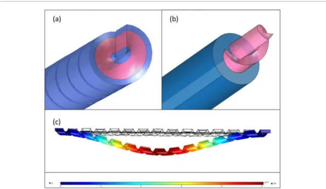
FEM simulations on the NS suspended and doubly clamped were carried out using a linear elastic behavior, which is a valid approximation when low forces are applied. Two geometrical configurations were considered: helical for thin metallic films and tubular for thicker metallic ones, both inside and outside the nanohelix or nanotubules, as shown in figure 5. The film was considered as pure platinum. Table 1 compares the quantitative results of AFM measurements to FEM simulations.
3.2.3. Results
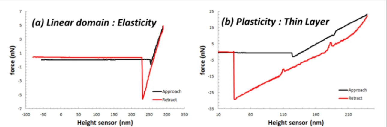
In a previous work [35], we have shown that compared to nanotubes of the same size and chemical nature, silica NS are rather soft (with stiffnesses around 0.1 N · m−1) with high fracture force (around 40 nN) and a large linear domain (300 nm).
Typical force–distance curves obtained from the hybrid NS are shown in figure 6. At small strains (figure
6(a)), the deflection remains linear and reproducible, which is consistent with an elastic behavior. At higher strains (figure 6(b)), a plastic deformation occurs, as shown by the hysteresis of the extension and retraction force curves. This hysteresis is even more pronounced for a thick metallic layer when further increasing the strain and eventually, fracture of the NS could be observed with a sudden drop of the signal at very high strain levels corre-sponding to forces ranging from 100 nN to 1 µN (to be compared to 40 nN for uncoated NS).
The experimental stiffnesses of the NS, originally ranging from 0.01 N · m−1 to 0.1 N · m−1 depending on the length of the NS, were significantly increased by the platinum coating, from 0.13 to 2.01 N · m−1. They were
Figure 5. COMSOL model of the metallized NS: (a) for a thin metallic layer (the helical shape is preserved), (b) for a thick metallic
layer (the helical shape is lost and the NS is transformed into a tube), (c) deflection of the NS in nanometers for an applied force of 10 nN.
Table 1. Comparison between AFM-measured (Kexp) and FEM-calculated (Ksimu) stiffnesses of metallized NS. The stiffnesses were taken
on the approach curve, at low force, before plasticity occurred.
Length (µm) Pt thickness (nm) Kexp (N · m−1) Ksimu (N · m−1)
0.53 1.0 0.98 1.13 0.54 3.0 1.40 2.33 0.58 4.0 2.01 2.44 0.78 4.0 0.13 0.73 0.90 4.0 0.53 0.51 1.10 4.5 0.14 0.34 1.16 3.0 0.18 0.20 1.16 5.5 0.36 0.23 1.23 3.5 0.25 0.19 1.25 2.5 0.23 0.14
7
S Habtoun et al
estimated from the approach curve, at low force, before plasticity occurred and summarized in table 1 with the FEM-simulated quantitative measurements.
The AFM mechanical measurements of a metallic NS showed a plasticity supported by the hysteresis between the approach and retract curves, and the irreversible decrease of its stiffness. This behavior was never observed on pure silica NS, which is linear in an elastic regime until rupture [34]. This shows that the metallic layer is ductile, despite its carbon impurities. The decrease of the stiffness corresponds to its plastic deformation.
The measured stiffnesses are shown in table 1 with their simulated counterparts. Some important discrepan-cies can be due to errors in estimating the lengths of the NS and the thicknesses of the metallic layer which can vary along the length inside and outside of the NS. Another possible reason could be the non-ideal mechanical clamping. Mechanical energy is lost through friction with the substrate, thus causing an apparent stiffening of the nanostructure. This effect has been studied and reported in [37–39] and is also supported by FEM simula-tions (see supporting information figures S7 and S8).
4. Conclusion
Our observations made during this study support the fact that FIB, despite the presence of impurities in the deposited layer, is a powerful prototyping method to transform flexible insulating helical nanostructures into metallic ones. It also allows to tune the stiffness of the NS while maintaining their mechanical properties: softness and a large linear domain, which are required for a successful implementation in NEMS. AFM measurements also give us insight into the forces applicable to unique nanostructures before irreversible damages occur, which is useful for future sensors applications. Based on these structural and mechanical studies, further works will be dedicated to the electromechanical characterization of the metallized NS for designing functional nanodevices.
Acknowledgments
This work was supported by the NANOSPRINGS project, Grant ANR-10-BLANC-0813, and by the NANOHELIFLEX project, Grant ANR-15-CE08-0041-03, of the Agence Nationale pour la Recherche (S Houmadi, and D Dedovets acknowledge the ANR for their grants) and partly by the French RENATECH network.
References
[1] Ren Z and Gao P X 2014 A review of helical nanostructures: growth theories, synthesis strategies and properties Nanoscale 69366–400
[2] McIlroy D N, Zhang D, Kranov Y and Norton M G 2001 Nanosprings Appl. Phys. Lett. 791540–2
[3] Wang Y, Xu J, Wang Y and Chen H 2013 Emerging chirality in nanoscience Chem. Soc. Rev. 422930–62
[4] Qin Y, Vogelgesang R, Eßlinger M, Sigle W, van Aken P, Moutanabbir O and Knez M 2012 Bottom-up tailoring of plasmonic nanopeapods making use of the periodical topography of carbon nanocoil templates Adv. Funct. Mater. 225157–65
[5] Esposito M, Tasco V, Todisco F, Cuscuna M, Benedetti A, Sanvitto D and Passaseo A 2015 Triple-helical nanowires by tomographic rotatory growth for chiral photonics Nat. Commun. 66484
[6] Seilis A, Moghadas H, Moez K and Daneshmand M 2015 Integrated magnetic nanoinductors IEEE Trans. Compon. Packag. Manuf.
Technol. 5675–84
[7] Lai X, Ding F, Xu X G, Wu W, Xu J and Hao Y 2008 Suspended nanoscale solenoid metal inductor with tens-nH level inductance Proc.
21st IEEE Int. Conf. on Micro Electro Mechanical Systems (Tucson, USA) pp 1000–4
[8] Peyer K E and Zhang L and Nelson B J 2013 Bio-inspired magnetic swimming microrobots for biomedical applications Nanoscale
51259–72
Figure 6. F–d curves taken on thin and thick metallized NS with an increased strain. (a) At small forces, a linear elastic behavior
is observed. (b) At higher forces, for a thin metallic layer, plasticity occurs as a hysteresis is clearly visible between the loading and unloading curves.
S Habtoun et al [9] Ghosh A and Paria D and Rangarajan G and Ghosh A 2014 Velocity fluctuations in helical propulsion: how small can a propeller Be
J. Phys. Chem. Lett. 562–8
[10] Dobrokhotov V V et al 2012 Thermal and optical activation mechanisms of nanospring-based chemiresistors Sensors 125608–22
[11] Hwang S, Kwon H, Chhajed S, Byon J W, Baik J M, Im J, Oh S H, Jang H W, Yoon S J and Kim J K 2013 A near single crystalline TiO2
nanohelix array: enhanced gas sensing performance and its application as a monolithically integrated electronic nose Analyst
138443–50
[12] Seto M W, Robbie K, Vick D, Brett M J and Khun L 1999 Mechanical response of thin films with helical microstructures J. Vac. Sci.
Technol. B 172172–7
[13] Gao P X, Ding Y, Mai W J, Hughes W L, Lao C S and Wang Z L 2005 Conversion of zinc oxide nanobelts into superlattice-structured nanohelices Science 3091700–4
[14] Zhang H F, Wang C M, Buck E C and Wang L S 2003 Synthesis, characterization, and manipulation of helical SiO2 nanosprings Nano
Lett. 3577–80
[15] Bell D, Sun Y, Zhang L, Dong L, Nelson B and Grützmacher D 2006 Fabrication and characterization of three-dimensional InGaAs/ GaAs nanosprings Nano Lett. 6725–9
[16] Brizard A, Aime C, Labrot T, Huc I, Berthier D, Artzner F, Desbat B and Oda R 2007 Counterion, temperature, and time modulation of nanometric chiral ribbons from gemini-tartrate amphiphiles J. Am. Chem. Soc. 1293754–62
[17] Zhang X et al 2017 Significantly enhanced mechanical properties in AlN helix Nanotechnology 28275703
[18] Liu L, Yoo S H, Lee S A and Park S 2011 Wet-chemical synthesis of palladium nanosprings Nano Lett. 113979–82
[19] Yang D, Carpena-Núñez J, Fonseca L F, Biaggi-Labiosa A and Hunter G W 2014 Shape-controlled synthesis of palladium and copper superlattice nanowires for high-stability hydrogen sensors Sci. Rep. 43773
[20] Caridad J M, McCloskey D, Rossella F, Bellani V, Donegan J F and Krstic V 2015 Effective wavelength scaling of and damping in plasmonic helical antennae ACS Photonics 2675–9
[21] Delclos T, Aimé C, Pouget E, Brizard A, Huc I, Delville M H and Oda R 2008 Individualized silica nanohelices and nanotubes: tuning inorganic nanostructures using lipidic self-assemblies Nano Lett. 81929–35
[22] Okazaki Y, Cheng J, Dedovets D, Kemper G, Delville M H, Durrieu M C, Ihara H, Takafuji M, Pouget E and Oda R 2014 Chiral colloids: homogeneous suspension of individualized SiO2 helical and twisted nanoribbons ACS Nano 86863–72
[23] Löw P, Kim B, Takama N and Bergaud C 2008 High-spatial-resolution surface-temperature mapping using fluorescent thermometry
Small 4908–14
[24] Frabboni S, Gazzadi G and Spessot A 2007 TEM study of annealed Pt nanostructures grown by electron beam-induced deposition
Physica E 37265–9
[25] Langford R, Wang T X and Ozkaya D 2007 Reducing the resistivity of electron and ion beam assisted deposited Pt Microelectron. Eng.
84784–8
[26] Botman A, Hesselberth M and Mulders J 2008 Improving the conductivity of platinum-containing nano-structures created by electron-beam-induced deposition Microelectron. Eng. 851139–42
[27] Batra N M, Patole S P, Abdelkader A, Anjum D H, Deepak F L and Costa P M 2015 Structural changes of electron and ion beam-deposited contacts in annealed carbon-based electrical devices Nanotechnology 26445301
[28] Koops H W P, Kaya A and Weber M 1995 Fabrication and characterization of platinum nanocrystalline material grown by electron-beam induced deposition J. Vac. Sci. Technol. B 132400–3
[29] Vila A, Hernandez-Ramirez F, Rodriguez J, Casals O, Romano-Rodriguez A, Morante J and Abid M 2006 Fabrication of metallic contacts to nanometre-sized materials using a focused ion beam (FIB) Mater. Sci. Eng. C 261063–6
[30] Xiong Q, Duarte N, Tadigadapa S and Eklund P C 2006 Force-deflection spectroscopy: a new method to determine the Young’s modulus of nanofilaments Nano Lett. 61904–9
[31] Qin Y, Kim Y, Zhang L, Lee S M, Yang R B, Pan A, Mathwig K, Alexe M, Gösele U and Knez M 2010 Preparation and elastic properties of helical nanotubes obtained by atomic layer deposition with carbon nanocoils as templates Small 6910–4
[32] Walters D A, Ericson L M, Casavant M J, Liu J, Colbert D T, Smith K A and Smalley R E 1999 Elastic strain of freely suspended single-wall carbon nanotube ropes Appl. Phys. Lett. 743803–5
[33] Cuenot S, Demoustier-Champagne S and Nysten B 2000 Elastic modulus of polypyrrole nanotubes Phys. Rev. Lett. 851690–3
[34] Houmadi S, Dedovets D, Si S, Tamoto R, Oda R, Delville M H and Bergaud C 2013 Determination of the elastic properties of SiO2
nanotubes templated from organic amphiphilic self-assemblies through inorganic transcription Appl. Phys. Lett. 102151904
[35] Houmadi S, Habtoun S, Dedovet D, Si S, Tamoto R, Oda R, Delville M and Bergaud C 2013 The 17th IEEE Int. Conf. on Solid-State
Sensors, Actuators and Microsystems Transducers and Eurosensors XXVII pp 952–5
[36] Drouin D, Couture A R, Joly D, Tastet X, Aimez V and Gauvin R 2007 Casino v2. 42: a fast and easy-to-use modeling tool for scanning electron microscopy and microanalysis users Scanning 2992–101
[37] Peng H B, Chang C W, Aloni S, Yuzvinsky T D and Zettl A 2006 Ultrahigh frequency nanotube resonators Phys. Rev. Lett. 97087203
[38] Ding W, Calabri L, Kohlhaas K M, Chen X, Dikin D A and Ruoff R S 2007 Modulus, fracture strength, and brittle versus plastic response of the outer shell of arc-grown multi-walled carbon nanotubes Exp. Mech. 4725–36
[39] Qin Q, Xu F, Cao Y, Ro P I and Zhu Y 2012 Measuring true Young’s modulus of a cantilevered nanowire: effect of clamping on resonance frequency Small 82571–6