HAL Id: hal-01382785
https://hal.archives-ouvertes.fr/hal-01382785
Submitted on 17 Oct 2016
HAL is a multi-disciplinary open access
archive for the deposit and dissemination of
sci-entific research documents, whether they are
pub-lished or not. The documents may come from
teaching and research institutions in France or
abroad, or from public or private research centers.
L’archive ouverte pluridisciplinaire HAL, est
destinée au dépôt et à la diffusion de documents
scientifiques de niveau recherche, publiés ou non,
émanant des établissements d’enseignement et de
recherche français ou étrangers, des laboratoires
publics ou privés.
Hybrid curved nano-structured micro-optical elements
A. Balčytis, D. Hakobyan, M. Gabalis, A. Žukauskas, D. Urbonas, M.
Malinauskas, R. Petruškevičius, E. Brasselet, S. Juodkazis
To cite this version:
A. Balčytis, D. Hakobyan, M. Gabalis, A. Žukauskas, D. Urbonas, et al.. Hybrid curved
nano-structured micro-optical elements. Optics Express, Optical Society of America - OSA Publishing,
2016, 24 (15), pp.10 - 24. �10.1364/OE.24.016988�. �hal-01382785�
Hybrid curved nano-structured micro-optical
elements
A. B
AL ˇCYTIS,
1,2,*D. H
AKOBYAN,
1,3,4M. G
ABALIS,
2A. Ž
UKAUSKAS,
5D. U
RBONAS,
2M. M
ALINAUSKAS,
5R. P
ETRUŠKEVI ˇCIUS,
2E. B
RASSELET,
3,4,6 ANDS. J
UODKAZIS11Centre for Micro-Photonics, Faculty of Engineering and Industrial Sciences, Swinburne University of
Technology, Hawthorn, VIC 3122, Australia
2Department of Laser Technologies, Center for Physical Sciences and Technology, Savanoriu Ave. 231,
LT-02300 Vilnius, Lithuania
3University of Bordeaux, LOMA, UMR 5798, F-33400 Talence, France 4CNRS, LOMA, UMR 5798, F-33400 Talence, France
5Department of Quantum Electronics, Physics Faculty, Vilnius University, Sauletekio Ave. 10, LT-10223
Vilnius, Lithuania
Abstract: Tailoring the spatial degree of freedom of light is an essential step towards the realiza-tion of advanced optical manipularealiza-tion tools. A topical challenge consists of device miniaturizarealiza-tion for improved performance and enhanced functionality at the micron scale. We demonstrate a novel approach that combines the additive three-dimensional (3D) structuring capability of laser polymerization and the subtractive subwavelength resolution patterning of focused ion beam lithography. As a case in point hybrid (dielectric/metallic) micro-optical elements that deliver a well-defined topological shaping of light are produced. Here we report on hybrid 3D binary spiral zone plates with unit and double topological charge. Their optical performances are compared to corresponding 2D counterparts both numerically and experimentally. Cooperative refractive capabilities without compromising topological beam shaping are shown. Realization of advanced designs where the dielectric architecture itself is endowed with singular properties is also discussed.
OCIS codes: (050.6875) Three-dimensional fabrication; (050.4865) Optical vortices; (130.3990) Micro-optical devices; (260.6042) Singular optics; (350.4855) Optical tweezers or optical manipulation.
References and links
1. M. Padgett and R. Bowman, “Tweezers with a twist,” Nature Photon.5, 343–348 (2011).
2. K. Dholakia and T. ˇCižmár, “Shaping the future of manipulation,” Nature Photon.5, 335–342 (2011).
3. M. Woerdemann, C. Alpmann, M. Esseling, and C. Denz, “Advanced optical trapping by complex beam shaping,” Laser Photon. Rev.7, 839–854 (2013).
4. P. Dannberg, F. Wippermann, A. Brückner, A. Matthes, P. Schreiber and A. Bräuer, “Wafer-level hybrid integration of complex micro-optical modules,” Micromachines5, 325–340 (2014).
5. M. Malinauskas, A. Žukauskas, V. Purlys, K. Belazaras, A. Momot, D. Paipulas, R. Gadonas, A. Piskarskas, H. Gilbergs, A. Gaidukeviˇci¯ut˙e, I. Sakellari, M. Farsari, and S. Juodkazis, “Femtosecond laser polymerization of hybrid/integrated micro-optical elements and their characterization,” J. Opt.12, 124010 (2010).
6. N. Yu and F. Capasso, “Flat optics with designer metasurfaces,” Nat. Mater.13, 139–150 (2014).
7. D. L. Andrews, Structured Light and Its Applications: an Introduction to Phase-Structured Beams and Nanoscale Optical Forces (Academic Press-Elsevier, 2008).
8. A. M. Yao and M. J. Padgett, “Orbital angular momentum: origins, behavior and applications,” Adv. Opt. Photon.3, 161–204 (2011).
9. N. B. Simpson, D. McGloin, K. Dholakia, L. Allen, and M. J. Padgett, “Optical tweezers with increased axial trapping efficiency,” J. Mod. Opt.45, 1943–1949 (1998).
10. M. A. Taylor, M. Waleed, A. B. Stilgoe, H. Rubinsztein-Dunlop, and W. P. Bowen, “Enhanced optical trapping via structured scattering,” Nature Photon.9, 669–673 (2015).
11. R. Dorn, S. Quabis, and G. Leuchs, “Sharper focus for a radially polarized light beam,” Phys. Rev. Lett.91, 233901 (2003).
12. J. Wang, J.-Y. Yang, I. M. Fazal, N. Ahmed, Y. Yan, H. Huang, Y. Ren, Y. Yue, S. Dolinar, M. Tur, and A. E. Willner, “Terabit free-space data transmission employing orbital angular momentum multiplexing,” Nature Photon.6, 488–496 (2012).
13. N. Bozinovic, Y. Yue, Y. Ren, M. Tur, P. Kristensen, H. Huang, A. E. Willner, and S. Ramachandran, “Terabit-scale orbital angular momentum mode division multiplexing in fibers,” Science340, 1545–1548 (2013).
14. L. Allen, M. W. Beijersbergen, R. J. C. Spreeuw, and J. P. Woerdman, “Orbital angular momentum of light and the transformation of laguerre-gaussian laser modes,” Phys. Rev. A45, 8185–8189 (1992).
15. G. Foo, D. M. Palacios, and G. A. Swartzlander, Jr., “Optical vortex coronagraph,” Opt. Lett.30, 3308–3310 (2005). 16. H. Liu, M. Q. Mehmood, K. Huang, L. Ke, H. Ye, P. Genevet, M. Zhang, A. Danner, S. P. Yeo, C.-W. Qiu, and J. Teng, “Twisted focusing of optical vortices with broadband flat spiral zone plates,” Adv. Opt. Mater.2, 1193–1198 (2014).
17. Y. Gorodetski, A. Drezet, C. Genet, and T. W. Ebbesen, “Generating far-field orbital angular momenta from near-field optical chirality,” Phys. Rev. Lett.110, 203906 (2013).
18. E. Brasselet, G. Gervinskas, G. Seniutinas, and S. Juodkazis, “Topological shaping of light by closed-path nanoslits,” Phys. Rev. Lett.111, 193901 (2013).
19. E. Brasselet, M. Malinauskas, A. Žukauskas, and S. Juodkazis, “Photo-polymerized microscopic vortex beam generators : precise delivery of optical orbital angular momentum,” Appl. Phys. Lett.97, 211108 (2010). 20. M. I. Shalaev, J. Sun, A. Tsukernik, A. Pandey, K. Nikolskiy, and N. M. Litchinitser, “High-efficiency all-dielectric
metasurfaces for ultracompact beam manipulation in transmission mode,” Nano Lett.15, 6261–6266 (2015). 21. E. Brasselet, N. Murazawa, H. Misawa, and S. Juodkazis, “Optical vortices from liquid crystal droplets,” Phys. Rev.
Lett.103, 103903 (2009).
22. C. Loussert, U. Delabre, and E. Brasselet, “Manipulating the orbital angular momentum of light at the micron scale with nematic disclinations in a liquid crystal film,” Phys. Rev. Lett.111, 037802 (2013).
23. D. Wu, J. Xu, L.-G. Niu, S.-Z.Wu, K. Midorikawa, and K. Sugioka, “In-channel integration of designable microoptical devices using flat sca↵old-supported femtosecond-laser microfabrication for coupling-free optofluidic cell counting,” Light: Sci. Appl.4, e228 (2015).
24. T. Gissibl, M. Schmid, and H. Giessen, “Spatial beam intensity shaping using phase masks on single-mode optical fibers fabricated by femtosecond direct laser writing,” Optica3, 448–451 (2016).
25. A. Žukauskas, M. Malinauskas, and E. Brasselet, “Monolithic generators of pseudo-nondi↵racting optical vortex beams at the microscale,” Appl. Phys. Lett.103, 181122 (2013).
26. D. Wen, F. Yue, G. Li, G. Zheng, K. Chan, S. Chen, M. Chen, K. F. Li, P. W. H. Wong, K. W. Cheah, E. Y. B. Pun, S. Zhang, X. Chen, “Helicity multiplexed broadband metasurface holograms,” Nat. Commun.6, 8241 (2015). 27. L. Huang, H. Mühlenbernd, X. Li, X. Song, B. Bai, Y. Wang, T. Zentgraf, “Broadband hybrid holographic
multiplex-ing with geometric metasurfaces,” Adv. Mater. doi:10.1002/adma.201502541 (2015).
28. L. Wei, Y. Gao, X. Wen, Z. Zhao, L. Cao, and Y. Gu, “Fractional spiral zone plates,” J. Opt. Soc. Am. A30, 233–237 (2013).
29. A. Žukauskas, G. Bataviˇci¯ut˙e, M. Šˇciuka, T. Jukna, A. Melninkaitis, and M. Malinauskas, “Characterization of photopolymers used in laser 3D micro/nanolithography by means of laser-induced damage threshold (LIDT),” Opt. Mater. Express4, 1601–1616 (2014).
30. A. Ovsianikov, J. Viertl, B. Chichkov, M. Oubaha, B. MacCraith, I. Sakellari, A. Giakoumaki, D. Gray, M. Vamvakaki, M. Farsari, and C. Fotakis, “Ultra-low shrinkage hybrid photosensitive material for two-photon polymerization microfabrication,” ACS Nano2, 2257–2262 (2008).
31. K. Y. Bliokh, E. A. Ostrovskaya, M. A. Alonso, O. G. Rodriguez-Herrera, D. Lara, and C. Dainty, “Spin-to-orbital angular momentum conversion in focusing, scattering, and imaging systems,” Opt. Express19, 26132 (2011). 32. A. S. Ostrovsky, C. Rickenstor↵-Parrao, and V. Arrizón, “Generation of the â ˘AIJperfectâ ˘A˙I optical vortex using a
liquid-crystal spatial light modulator,” Opt. Lett.38, 534–536 (2013).
33. E. Brasselet, “Optical vortices from closed-loop subwavelength slits,” Opt. Lett.38, 2575–2577 (2013).
34. G. Gervinskas, G. Seniutinas, and S. Juodkazis, “Control of surface charge for high-fidelity nanostructuring of materials,” Laser Photon. Rev.7, 1049–1053 (2013).
35. M. Malinauskas, A. Žukauskas, S. Hasegawa, Y. Hayasaki, V. Mizeikis, R. Buividas, and S. Juodkazis, “Ultrafast laser processing of materials: from science to industry,” Light: Sci. Appl.5, e16133, doi:10.1038/lsa.2016.133 (2016).
1. Introduction
Advanced optical manipulation of matter at the microscopic scale implies the development of optical elements enabling on-demand structuring of electromagnetic fields [1–3]. Significant progress in the miniaturization of optical systems has been made by combining multiple opti-cal functions within a single structure. An example of the trend towards miniaturization and hybridization is the lithographic fabrication of micro-lens arrays for multi-spot illumination or multi-aperture detectors. Photoresist reflow method is employed to create micro-lenses with
a subsequent laser writing step used to inscribe a di↵ractive phase correction element [4]. Such hybridization is pursued either to circumvent limitations in fabrication method, as in the aforementioned example, or when additional flexibility is required for specific fields. Fabrication methods need to be even more adaptive for applications such as optical sorting in microfluidics. For such purposes laser photopolymerization allows to depart form the 2D geometry imposed by lithographic approaches and create complex 3D optics [5]. Since this method is inherently capable of additively producing arbitrary refractive dielectric structures, further hybridization requires an approach with complimentary capabilities. In contrast, subtractive focused ion beam (FIB) milling of metals is capable of creating complex di↵ractive elements and metasurfaces with unmatched precision [6]. Since in such elements metal films and shells are sub-wavelength in thickness as well as in their patterning resolution, they provide a way to complement laser polymerized bulk refractive structures.
One of the areas where new methods to compound optical functionality and enact minia-turization are in high demand is light structuring. Structured light, also named complex light, refers to optical fields that possess non-trivial spatial distribution of one or several characteristics such as intensity, phase or polarization. Its description and main applications have been already extensively reviewed within the past decade, see for instance refs. [7, 8], and it still attracts growing attention from the optics and photonics community. A few paradigmatic examples are worth mentioning to appreciate the impact of structured light, especially when optical phase structuring is considered. In optical trapping, it is known since almost two decades that light beams endowed with optical phase singularities (i.e. vortex beams), which correspond to a local electric field amplitude proportional to exp(i` ) with the azimuthal angle and ` the integer topological charge, allow enhancement of the axial trapping efficiency [9]. Nevertheless, phase structuring continues to amaze as demonstrated just recently with the drastic increase of transverse trapping efficiency [10]. Sharper focus has been achieved for radially polarized light beams that consist of a superposition of contra-circularly polarized vortex beams with opposite unit topological charges [11]. Vortex beams also provide a spatial (orbital) degree of freedom that adds to the one associated with the polarization state (spin) of light. The fact that the orbital degree of freedom has an unbound set of eigenstates formally has demonstrated great promise in optical communications [12, 13]. This also provides with enhanced optomechanical capabilities since a vortex beam with topological charge ` carries `~ angular momentum per photon [14] whereas the spin contribution is limited to ±~ angular momentum per photon. Optical imaging is another topic that has been deeply impacted by phase structuring. At the microscopic scale, this has been celebrated in 2014 with Nobel Prize in Chemistry for the development of super-resolved fluorescence microscopy. On the other hand, astronomical observations now benefit from optical vortex coronagraphy developed ten years ago [15]. As such, it seems not exaggerated to say that engineering of light beams has revolutionized our ways of taming light and current technological developments are likely to bring further unexpected surprises in the future.
Conventional methods to generate vortex beams involve the use of spatial light modulators, forked di↵raction gratings, phase plates or mode converters [8]. However, recent e↵orts to achieve optical trapping and manipulation at the microscale resulted in forgoing bulky options in favor of miniaturized structures, such as spiral zone plates (SZP) of both di↵ractive [16] and plasmonic [17] varieties, topological nanoslits [18], photopolymerized structures [19], metasurface-based devices [6, 20], or self-engineered birefringent objects [21, 22]. On the other hand, ultrafast laser 3D nanolithography o↵ers unmatched structuring flexibility on non-flat surfaces such as optical fiber tips [5] or inside buried microfluidic channels [23]. It makes it a practical choice for custom-on-demand 3D printing of microoptics [24].
Although optical manipulation setups realized at the microscale provide for added versatility and integration, new fabrication challenges also arise when multi-functional behavior is needed. In that case, multiplexing structures achieving independent optical operation into a single
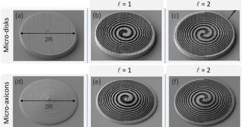
multi-2R (a) (d) (f) (b) (c) (e) = 1 Mi cr o -di sk s = 2 = 1 Mi cr o -a xi cons = 2 2R
Fig. 1. SEM images of photopolymerized flat disk pedestal (a) an axicon with 165 full-apex angle (d) structures of diameter 2R = 30 µm after sputter-coating with 200 nm of Au. SEM images of the same structures after FIB milling of SZP patterns with vortex orders ` = 1 (b,e) and ` = 2 (c,f) in the Au layer.
functional architecture is an option. One can mention the monolithic integration of dielectric spiral phase plates and axicons fabricated by 3D photopolymerization into helical axicons in order to generate higher-order Bessel beams [25]. Also noteworthy is the very recent realization of multiplexed 2D metallic metasurface holograms [26, 27]. Here we propose to combine the additive 3D structuring capability of laser photopolymerization and the subtractive subwavelength resolution patterning of focused ion beam lithography to produce hybrid (dielectric/metallic) micro-optical elements for the purpose of topological shaping of light. Our demonstration relies on the fabrication of hybrid 3D binary SZPs enabling the generation of single-charge and double-charge optical vortices. We show, both numerically and experimentally, the cooperative refractive interaction between the individual 2D metallic and 3D dielectric sub-parts without compromising topological beam shaping from the SZP. Also, we discuss advanced 3D designs where the dielectric architecture itself is endowed with singular properties and report on their fabrication. Our results suggest that additive manufacturing methods such as 3D direct laser writing, once combined with state-of-the-art nanofabrication technologies, pave the way towards the realization of 3D hybrid metasurfaces of arbitrary complexity.
2. Design and fabrication of hybrid 3D singular micro-optics
The design of a SZP combines the radial Hilbert transform operation with Fresnel zone plate focusing, which gives rise to a focused vortex beam in transmission. It is described by a 2D binary transmittance function t of the form [28]:
t(r, ') = { 0 if (2k 1)⇡ `' ⇡r
2
f 2k⇡1 if 2k⇡ `' ⇡r2
f (2k + 1)⇡, (1) where (r, ') refer to the polar coordinates, is the wavelength, f is the e↵ective focal length of the SZP and index k = (0, 1, 2, ...) is the spiral zone number. Designed SZP were chosen to have a diameter of 2R = 30 µm which gives up to 10 zones.
Experimentally, 3D SZPs designed with focal length f = 18 µm and ` = (1, 2) following Eq. (1), are fabricated by means of FIB lithography milling through an optically opaque layer of Au. The large depth-of-focus of the FIB allows to pattern metal layers overlaying various 3D
structures. In the present work milling was done through Au coatings on both flat disk and axicon pedestals, each created by direct laser writing using femtosecond laser nano-polymerization. Axicons were used in this first study to evaluate whether focused ion beam lithography is viable for 3D fabrication of complex patterns without changing the focusing parameters. Similarly, flat disk pedestals represent a planar reference.
The first stage of fabrication involves photopolymerization of the disk or cone shaped pedestal by direct laser writing. A hybrid organic-inorganic photopolymer SZ2080 doped with Irgacure 369 photoinitiator at 2 wt.% [29] is chosen as the material for the pedestal. This polymer is particularly suitable for fashioning various micro-optical structures. Indeed, it is known to possess the required mechanical robustness as well as a refractive index closely matched to that of glass in the visible spectral region (nSZ2080=1.504, nGlass=1.52) [30]. Prior to laser exposure the
photoresist is prepared by drop-casting SZ2080 onto a cover-glass substrate that defines the (x, y) plane followed by pre-baking on a hotplate for 60 min at 90 C. Direct-write fabrication is conducted using a Yb:KGW (PHAROS, Light Conversion Ltd.) laser with 300 fs optical pulse duration at second harmonic ( = 515 nm), 200 kHz repetition rate, under tight focusing conditions using a 63⇥, N A = 1.4 microscope objective (Carl Zeiss). The 15 µm radius 3D flat disk pedestal structures are produced under 70 µW average power with corresponding pulse energy of 0.35 nJ and 0.988 TW/cm2intensity per pulse at focus, using a 0.5 mm/s scanning
velocity along raster trajectories with 50 nm voxel overlap. Conversely, the axicon structures with a full apex angle of 165 are fabricated using 27.5 µW average power (0.14 nJ, 0.388 TW/cm2)
at 0.1 mm/s scanning velocity along spiral trajectories with 50 nm voxel overlap. Photopolymer development is performed by immersing it into pure 4-methyl-2-pentanone for 1 h to remove any unexposed residue.
The resulting photopolymerized structure is then coated with a 200 nm thick Au film using magnetron sputtering (AXXIS, JKLesker). Binary patterns given by Eq. (1) are transferred onto the Au sputtered polymerized structures by means of FIB milling, using a Raith IonLINE ion beam lithography tool. An interferometrically controlled piezoelectric stage as well as FIB imaging capability allow for precise control over the positioning of the pedestal structures for spiral pattern transfer. After alignment a 35 kV Ga+ion beam is focused down to a 25 nm diameter
spot and set to scan along the desired pattern until the 200 nm Au layer was selectively stripped over 104 sequential patterning loops. The binary transmission patterns are thus reproduced
with high fidelity, closely approximating the geometric parameters deduced from numerical simulations. This is illustrated in Fig. 1 where SEM images of the structures before and after FIB milling are shown in panels (a) and (d), and in panels (b), (c), (e) and (f), respectively. These images reveal the presence of residual gold islands in the milled areas that most likely result from impurities on the surface of the polymerized pedestal acting as crystallization sites for the sputtered gold. Such nanoscale islands are more resilient to ion bombardment than the rest of the structure.
3. Numerical simulations and experimental results
The optical behavior of the fabricated 3D SZPs is simulated numerically by using a commercially available FDTD software package (FDTD Solutions, Lumerical Solutions, Inc.). The simulation structure for the hybrid micro-optical elements is defined by applying a gold layer with 200 nm thickness (using the refractive index nmetal=0.5106 + i 2.2495) and spiral patterns defined by Eq. (1) onto a dielectric (using the refractive index ndielectric=1.504) axicon and a flat pedestal for reference. Two simulations are performed for each structure, namely by using x-polarized and y-polarized plane waves at wavelength = 532 nm impinging at normal incidence (along the z axis) from the substrate side. By doing so, the response to an arbitrary polarized illumination can be deduced from the linear superposition principle by using appropriate complex weighting factors. In addition, the simulation box x ⇥ y ⇥ z dimensions are 44 µm ⇥ 44 µm ⇥ 34 µm and
its surface boundaries are ended by perfectly matched layer boundaries to prevent from spurious e↵ects of reflections from the finite-size calculation volume. A non-uniform meshing algorithm was used. The mesh grid sizes varied from 10 nm close to the metal surface to 60 nm at remote regions of the simulation, with the average cell size being at around 30 nm.
Simulation results are compared with experimental optical characterization of the fabricated structures, which involves the propagation features of the transmitted light field. In practice, the structures are illuminated at normal incidence from substrate side by a 532 nm wavelength Gaussian laser beam, focused using a low numerical aperture lens, the sample being placed in the focal plane of the lens. Considering that the gold layer is thick enough to act as an almost opaque layer, we choose a beam waist radius w0twice larger than the radius R of the structure, which
thus mimics plane wave illumination. If the metal layer was not opaque enough, a significant portion of laser radiation could be transmitted through the flat gold film surrounding the 3D
Simulation
1 μmExperiment
16 0 4 8 12 -16-12 -8 -4 z (µ m) x (µm)f
16 0 0 4 8 12 -16-12 -8 -4 z (µ m) x (µm)f
1 μm= 1
= 2
15 0 5 10 20 15 5 10 20(a)
(b)
(d)
(c)
(f)
(e)
θ
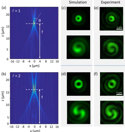
Fig. 2. (a,b) FDTD simulated total intensity cross-sections in the meridional plane (x, z) for ` = 1 (a) and ` = 2 (b) in the case of left-handed circularly polarized incident light on flat SZPs. (c,d) Total intensity (x, y) cross-section in the focal plane (top panel) and corresponding interference pattern that results from the coherent superposition with a co-axial Gaussian beam (bottom panel) ` = 1 (c) and ` = 2 (d). (e,f) Experimental counterpart of panels (a) and (b), respectively.
polymerized structures. As this light would have a phasefront that is di↵erent than the one shaped by the refractive pedestals it could distort the optical characterization results. The issue regarding the opacity of the gold layer is checked in simulations by replacing gold by a so-called perfect electric conductor (PEC) material with infinite conductivity ! 1 that expectedly mimics perfect binary amplitude mask given by Eq. (1) better than the metallic mask does. Numerically, in Lumerical FDTD software simulations, PEC was set as a material with refractive index nPEC=710 + i 710, whereas for analytical calculations ! 1 enters as the imaginary part of permittivity. Identical results are found regardless of whether Au or PEC values are used. In practice, the optical intensity profiles at a distance z from the plane of the structure are recorded by means of a microscope objective (100⇥, N A = 0.8) and a CCD camera. On the
other hand, information on the phase profiles are unveiled by recording interference patterns that result from the superposition of the transmitted field with a collinear Gaussian reference arm.
Finally, we note that we are purposely restricting our investigations to the particular case of incident circular polarization for both simulations and experiments. Indeed, present use of micro-optical structures leads to transmitted light whose non-paraxial features cannot be ignored. Hence it is fitting to use the circular polarization basis as it allows to address the ensuing coupling between the polarization state and spatial degrees of freedom (i.e. the so-called spin-orbit interaction of light) with ease.
3.1. Two-dimensional spiral zone plates
In the case of flat SZP structures, see Figs. 1(b) and 1(c), numerical FDTD simulations of the transmittance of left-handed circularly polarized light (see appendix for used field representation convention) predict strong focusing behavior, as expected from the designed focal length f = 18 µm recalling that R = 15 µm. Calculations give slightly lower focal distance, f = 16.4 µm with no noticeable e↵ect of the helicity =±1 of the incident circularly polarized light. This is illustrated in Figs. 2(a) and 2(b) that show total intensity cross-sections in the meridional plane (x, z) for ` = (1, 2). These intensity patterns emphasize similar focusing distance whatever ` that can be associated to a nominal numerical aperture of the elements, N A = sin ✓ ⇡ 0.67, based on the “viewing angle” of the structure ✓ = arctan(R/f ). For comparison, we find f = 19 µm in the case of a flat pedestal with ` = 0 whatever the value of . The latter discrepancies between the designed focal distance and the calculated ones might be explained by residual form birefringence arising from metallic layer structuring (though not subwavelength).
In the focal plane of the SZP, doughnut-like intensity pattern is predicted both for ` = (1, 2). This is reminiscent of the generated optical vortices whose respective unit and double topological charge are clearly exhibited by one-arm and two-arm spiraling interference patterns obtained from the coherent superposition with a co-axial Gaussian beam, see Figs. 2(c) and 2(d). In addition, we note the increase of the radius of the doughnut shaped intensity pattern with |`| as expected from the well-knownp`-behavior of Laguerre-Gaussian-like beams. Indeed, quantitatively, intensity ring diameters are ⇠ 1.4 µm and ⇠ 2.1 µm for ` = 1 and ` = 2, respectively. Such a behavior is actually retrieved experimentally, as shown in Figs. 2(e) and 2(f) that nicely matched with their simulation counterparts. In particular, we find intensity ring diameters ⇠ 1.3 µm and ⇠ 2.0 µm for ` = 1 and ` = 2, respectively. Also we note that the handedness of the interference spiraling pattern does not depend on incident field polarization as expected from the scalar nature of the SZP design.
Noticeably, experimentally observed broken axisymmetry of the intensity pattern in the focal plane (see top panels of Figs. 2(e) and 2(f)) is not a spurious manifestation of instrumental limitations. Indeed, 1-fold and 2-fold rotational symmetry is found in simulations as shown in top panels of Figs. 2(c) and 2(d). Its origin is attributed to the finite size of the SZPs whose `-arm design is unavoidably associated with ` abrupt ends at the periphery of the structure, as one can see from SEM images in Fig. 1. This is supported by further simulations made on
z L R tot σ = -1 ℓ = 1 σ = +1ℓ = 1 σ = -1ℓ = 2 σ = +1ℓ = 2 (a) (b) (c) (d) 1 μm 1 μm 1 μm 1 μm 0 2π
Fig. 3. FDTD simulations of the vectorial content of light in the focal plane of flat SZP structures with ` = 1 [columns (a) and (b)] and ` = 2 [columns (c) and (d)] for both right-handed ( = 1) and left-right-handed ( = +1) incident circular polarization. Both intensity (left part of each column) and phase (right part of each column) of total (‘tot’), right-handed circular (‘R’), left-handed circular (‘L’), and longitudinal (‘z’) contributions to the total electric field are shown. Bottom-right colormap refers to phase from 0 to 2⇡.
structures with larger sizes. Indeed, broken axisymmetry of the total intensity patterns in the (x, y) plane tends to vanish as the radius R of the SZP increases, which implies a practical trade-o↵ between axisymmetry and fabrication time. However, experimental results show a somewhat lower axisymmetry than predicted by simulations. This is in part due to the Gaussian beam used in experiment, which is only an approximation of the plane wave used in simulations. Fabrication imperfections are likely to also have an e↵ect, especially at the structure edges where the narrowest groves are defined. Finally, beam alignment in experiment produces additional sources of error the FDTD simulations are not susceptible to.
Remarkably, such SZPs behave as high-N A micro-optical elements whose N A increases with wavelength as expected from the f factor in Eq. (1). As such, the transmitted light has nonparaxial features that are easily deciphered by FDTD simulations. This is illustrated in Fig. 3, where the full vectorial nature of light is analyzed in the focal plane of flat SZP structures with ` =1 [columns (a) and (b)] and ` = 2 [columns (c) and (d)] for both right-handed ( = 1) and left-handed ( = +1) circularly polarized incident field. For ` = (1, 2), nonparaxial features can be straightforwardly grasped by mere inspection of the doughnut-like total intensity pattern by noting that the on-axis intensity is nonzero or zero depending on the incident circular polarization helicity =±1, see upper row of Fig. 3. This is reminiscent to the fact that both the contra-circularly polarized (with respect to the input polarization state) and the longitudinal components of the output field are nonzero and may exhibit on-axis intensity. This is detailed in the three rows of Fig. 3 labeled ‘R’, ‘L’ and ‘z’, which respectively refer to right-handed circular, left-handed circular and longitudinal contributions to the total electric field. As a rule of thumb, the longitudinal field component carries an optical phase singularity of topological charge ` + while the spatial distribution of the phase of the contra-circular component is associated with a topological charge ` + 2 , as one can ascertain from the phase profiles in Fig. 3. This is a consequence of the spin-orbit interaction of light resulting from the scattering of light [31] by
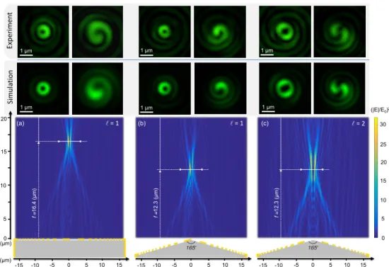
0 5 10 15 -15 -10 -5 -15 -10 -5 0 5 10 15 0 5 10 15 20 0 30 (a) (b) z (µm) x (µm) (|E|/E0)2 165ᵒ 15 20 25 10 5 5 10 15 -15 -10 -5 0 165ᵒ (c) Si mul ati on Experi me n t f = 12. 3 (µ m ) f = 16. 4 (µ m ) f = 12. 3 (µ m ) = 1 = 1 = 2 1 μm 1 μm 1 μm 1 μm 1 μm 1 μm
Fig. 4. FDTD simulated total intensity cross-sections in the meridional plane (x, z) in the case of left-handed circularly polarized incident light on flat pedestal for ` = 1 (a), and axicon pedestal with 165 full apex angle for ` = 1 (b) and ` = 2 (c). Top panels refer to the confrontation between simulation and experiment for both total intensity (x, y) cross-section in the focal plane (left side) and corresponding interference pattern that results from the coherent superposition with a co-axial Gaussian beam (right side). Bottom line: sketches of the side view of the 2D and 3D SZPs.
SZPs and is reminiscent of total angular momentum conservation. 3.2. Three-dimensional spiral zone plates
Analysis of 3D SZPs is performed similarly to above 2D case. A comparative study is presented in Fig. 4 in the case ` = 1, as shown in panels (a) and (b). The 3 µm height flat pedestal does not appreciably change the focusing behaviour of the SZP element. FDTD simulations show that the amount of bulk material in the pedestal does not a↵ect the focusing performance of the device, as it only imparts some collective phase o↵set. However, di↵erences in optical path length due to the curved surface of the axicon induces changes. The qualitative di↵erence between these two cases is the prediction of a substantial decrease of the focal length from f ⇡ 16.4 µm down to f ⇡ 12.6 µm, taking the top surface of the 2D SZP and the tip of the 3D SZP as the origin from which is evaluated the focal length. Such a trend is retrieved experimentally, indeed we observe a decrease of the focal length from f = 20 ± 2 µm down to f = 15 ± 2 µm (precision of the used translation stage prevents claiming a better accuracy).
Interestingly, the latter decrease of focal length can be also assessed without need of numerics by mere evaluation of the combined optical powers of the 3D refractive dielectric and the 2D di↵ractive metallic elements taken separately. Namely, f 1
hybrid= fdielectric1 + fmetallic1 where firefers
to the focal length of the element “i”. On the one hand, we recall that the focal distance of the 2D SZP defined by Eq. (1) is designed for fmetallic=18 µm. On the other hand, the focal for an
(b)
(a)
(c)
Hei
gh
t
50 μm
Fig. 5. (a) Three-dimensional illustration of the design of a topological pyramid of height H, where the basis corresponds to a sixth-order hypocycloid curve inscribed in a circle of radius R. Side-view and top-view SEM images of such a pyramid fabricated by laser photopolymerization for R = H = 50 µm are shown in panels (b) and (c), respectively.
focal distance, fdielectric = zmax/2 = R/[2(n 1)↵] [25], which gives fdielectric ⇡ 114 µm in
present case. One thus gets fhybrid⇡ 15.5 µm, which corresponds to a 14% decrease that should
be compared to the 23% decrease predicted by FDTD simulations. A decrease of focal distance of the SZP could be achieved in a planar geometry by decreasing the focal distance parameter f in Eq. (1). However, as the focal distance is decreased the SZP pattern needs to be scaled down accordingly, along with corresponding increases to FIB patterning fidelity requirements. Therefore, a refractive subcomponent is especially useful in creating high-N A structures, where the hyperbolic dependence on focal distance f could create challenges for planar FIB fabrication.
Finally, intensity and phase characteristics in the focal plane of 3D SZPs with ` = 1 and ` = 2 are also analyzed experimentally and compared with numerical simulations, as shown in the upper row of Fig. 4. Both experimental and simulation results hint at axicon pedestals slightly shrinking down the annular focal spot. Observations suggest that the hybrid axicon/SZP structure is a way to create â ˘AIJperfect optical vorticesâ ˘A˙I whose dark hollow radius does not depend on the topological charge [32] by appropriately selecting the full apex angle of the axicon. However, the e↵ect is not very prominent in this first study, therefore, further work is forthcoming.
The transmittance of the spiral zone structure has been evaluated based on numerical sim-ulations. The total transmittance through the 30 µm diameter structures is T ⇡ 22.5% for flat pedestal structures and T ⇡ 25% for patterned cones. This is in part due to the 50% opacity of the metal pattern, the suppression of transmittance through sub-wavelength (aspect ratio of 1) slits as well as the di↵ractive nature of the pattern itself. However, if the Poynting vector is integrated only in the R ⇡ 2 µm focal spot region, transmittance values become T ⇡ 5.1% for flat pedestal structures and T ⇡ 5% for patterned cones. The influence of the photopolymerized pedestals on the total losses is only marginal.
In addition to the aforementioned refractive modifications, the proposed hybrid polymerisation and FIB milling design is useful for applications in microscopy and microfluidics where only an optical vortex beam should be generated with blocked light which does not pass through the binary transmission mask. This creates beneficial dark-background imaging in microscopy setting or a well-defined focused optical vortex in microfluidic channel for trapping/sorting applications. The flat pedestal design is appealing for easier integration into practical microfluidic chip with polymerised functional structures and for creating specific phase o↵sets.
Above demonstration of principle that 3D SZPs of good quality can be fabricated by combining 3D laser polymerization to focused ion beam lithography of ultrathin metallic films sets the basis for the development of arbitrary hybrid curved metasurfaces. In particular, one can consider the realization of advanced designs where the dielectric architecture itself is endowed with singular features. An example is provided in Fig. 5 that shows the design and SEM images of a cuspy pyramid, where the basis corresponds to a continuous deformation of the circle with
six-fold rotation symmetry that belongs to the family of hypocycloid curves. This example thus corresponds to a 3D design endowed with cusp singularities that possesses a convex counterpart generated from epicycloid curves. FIB milling can be used to further add sub-wavelength size incisions (either through a metal mask or directly into the polymer) with presission beyond that of laser photopolymerization to further complement its functionality. From previous works dealing with cuspy 2D designs [18, 33] that showed intriguing capabilities regarding the generation of optical phase singularities, 3D singular designs are likely to bring a new twist to beam engineering.
4. Conclusion
We have reported on the realization and analysis of hybrid 3D micro-optical elements enabling optical phase engineering by combining 3D dielectric structures obtained from laser polymer-ization to subwavelength-thick metallic film patterned by focus ion beam milling. As such, this represent an original attempt to produce hybrid curved metasurfaces. Demonstration has been carried out in the particular case of 3D binary spiral zone plates with unit and double topological charge, whose optical performances are compared to their 2D counterparts both numerically and experimentally. This work illustrates how fabrication techniques combining refractive and di↵ractive optical approaches can jointly lead to the elaboration of multifunctional of optical elements at the microscale, possibly endowed with topological shaping capabilities. State of the art nanofabrication tools also allow realizing more complex designs where both the dielectric and metallic sub-parts can possess singular features, which may open enhanced engineering of optical singularities and ensuing development of optical techniques based on singular optics.
Here we demonstrated the unique merit of FIB beam milling due to long depth-of-focus by patterning on a 3D surface of an axicon. Fast and accurate FIB milling becomes feasible at high fabrication throughput by mitigation of surface charging [34]. Combination of the direct laser and ion-beam writing methods is promising for novel applications in 3D micro- and nano-photonics [35].
Appendix
We used the following convention for the complex representation of the optical field. Namely, a fully polarized plane wave propagating towards z > 0 is expressed asE = E0ei(kz !t)e, where k
is the wavevector, ! is the angular frequency ande is the unit vector that defines the polarization state. In the present work, we consider both left-handed and right-handed circular polarization states that corresponds toe = (x + iy)/p2 with =±1, respectively. In addition, a beam carrying an optical phase singularity of topological charge ` corresponds to a field amplitude proportional to the pure phase factor exp(i` ) where is the polar angle in the plane (x, y). Ensuing angular momentum characteristics (within the paraxial approximation) are ~ spin angular momentum per photon carried bye -polarized light and `~ orbital angular momentum per photon carried by light field with amplitude proportional to exp(i` ).
Acknowledgments
This work was partially supported by the Australian Research Council Discovery grant DP130101205 and the Linkage grant LP120100161 with Raith-Asia. DH and EB acknowledge support by the French State in the frame of the “Investments for the future” Programme IdEx Bordeaux (reference ANR-10-IDEX-03-02). AZ and MM acknowledge funding by the Research Council of Lithuania under the Lithuanian-French Programme "Gilibert" (No. TAP LZ-4/2015). SJ acknowledges the startup funding of the Nanotechnology facility by strategic funding from Swinburne University. FDTD simulation work was performed on the swinSTAR supercomputer at Swinburne University of Technology.
![Fig. 3. FDTD simulations of the vectorial content of light in the focal plane of flat SZP structures with ` = 1 [columns (a) and (b)] and ` = 2 [columns (c) and (d)] for both right-handed ( = 1) and left-handed ( = +1) incident circular polarization](https://thumb-eu.123doks.com/thumbv2/123doknet/14471194.522373/9.918.180.737.139.439/simulations-vectorial-content-structures-columns-incident-circular-polarization.webp)