HAL Id: hal-02011640
https://hal.univ-lorraine.fr/hal-02011640v2
Submitted on 8 Feb 2019
HAL is a multi-disciplinary open access
archive for the deposit and dissemination of
sci-entific research documents, whether they are
pub-lished or not. The documents may come from
teaching and research institutions in France or
abroad, or from public or private research centers.
L’archive ouverte pluridisciplinaire HAL, est
destinée au dépôt et à la diffusion de documents
scientifiques de niveau recherche, publiés ou non,
émanant des établissements d’enseignement et de
recherche français ou étrangers, des laboratoires
publics ou privés.
Electrical transport properties of black phosphorus
based field-effect transistor with Au/Co/MgO tunneling
contacts
Shiheng Liang, Huaiwen Yang, Abdelhak Djeffal, Bingshan Tao, Stefan
Mc-Murtry, Stéphane Mangin, Yuan Lu
To cite this version:
Shiheng Liang, Huaiwen Yang, Abdelhak Djeffal, Bingshan Tao, Stefan Mc-Murtry, et al.. Electrical
transport properties of black phosphorus based field-effect transistor with Au/Co/MgO tunneling
contacts. Journal of Applied Physics, American Institute of Physics, 2017, 122 (16), pp.164301.
�hal-02011640v2�
J. Appl. Phys. 122, 164301 (2017); https://doi.org/10.1063/1.5000524 122, 164301 © 2017 Author(s).
Electrical transport properties of black
phosphorus based field-effect transistor with
Au/Co/MgO tunneling contacts
Cite as: J. Appl. Phys. 122, 164301 (2017); https://doi.org/10.1063/1.5000524
Submitted: 16 August 2017 . Accepted: 10 October 2017 . Published Online: 23 October 2017
Shiheng Liang, Huaiwen Yang, Abdelhak Djeffal, Bingshan Tao, Stefan Mc-Murtry, Stéphane Mangin , and Yuan Lu
ARTICLES YOU MAY BE INTERESTED IN
Tunneling field effect transistor integrated with black phosphorus-MoS2 junction and ion gel dielectric
Applied Physics Letters 110, 033103 (2017); https://doi.org/10.1063/1.4974303 Electric field effect in ultrathin black phosphorus
Applied Physics Letters 104, 103106 (2014); https://doi.org/10.1063/1.4868132 A sub-thermionic MoS2 FET with tunable transport
Electrical transport properties of black phosphorus based field-effect
transistor with Au/Co/MgO tunneling contacts
ShihengLiang,HuaiwenYang,AbdelhakDjeffal,BingshanTao,StefanMc-Murtry,
St!ephaneMangin,and YuanLua)
Institut Jean Lamour, UMR 7198, CNRS-Universit!e de Lorraine, BP 239, 54506 Vandœuvre, France
(Received 16 August 2017; accepted 10 October 2017; published online 23 October 2017)
Black phosphorus (BP) has recently emerged as a promising two-dimensional direct bandgap semi-conducting material. Here, we report the fabrication and the electrical transport measurements of the black phosphorus based field-effect transistor with the Au/Co/MgO as drain and source tunnel-ing contacts. By modulattunnel-ing the back-gate voltage, the multilayer black phosphorus channel exhib-its ambipolar characteristics (bothn-type and p-type) and the conduction behavior can be switched from hole dominated to electron dominated transport region. In the hole dominated region, we have measured a minimum of Schottky barrier height of 37 meV for Au/Co/MgO contact on BP. Moreover, the transistor ON/OFF (Ion/Ioff) ratio is obtained as large as 107 at 20 K and 105 at
300 K. A systematic study of the temperature and the back-gate voltage dependent conduction properties has been performed to understand the modulation of band structure and the ambipolar behavior. The demonstration of high ON/OFF ratio and low Schottky barrier height by using Au/Co/MgO tunneling contacts reveals a promising potential for spintronics applications with mul-tilayer black phosphorus field-effect transistor.Published by AIP Publishing.
https://doi.org/10.1063/1.5000524
I. INTRODUCTION
Two-dimensional (2D) materials with atomic thickness have been recently unveiled as an important family of materi-als in physics and materimateri-als science.1–9Since the discovery of graphene in 2004,1a fair amount of research has been dedi-cated to fabricate other thin layer 2D materials, for examples of boron nitride10 and transition metal dichalcogenides (TMDs) materials.3–9The understanding of physics and mate-rial characteristics of 2D matemate-rials leads to the possibility of many applications, such as transistors,7,9 optoelectronics,11 sensors,12 photovoltaics,13 medicine,14and energy storage.15 In the 2D material family, graphene is known as a semicon-ductor with zero bandgap. Despite its high mobility, the gra-phene is not suitable to be used as field-effect transistors (FETs)1,2 due to the zero bandgap. Another 2D material is boron nitride, which is an insulator and can be used as a tun-nel barrier in 2D-heterostructure device to improve the physi-cal properties.10Besides the above two types of 2D materials, TMDs such as MoS2, WSe2, and MoSe2have semiconducting
properties and can play the role of drain-source channel in FETs, but their mobility is relatively low.3–9
Recently, black phosphorus (BP) has attracted a large amount of attention and emerged as an important 2D mate-rial due to its interesting physics properties.16–24The BP has a layer stacked structure by van der Waals interactions. The monolayer (ML) BP has a direct bandgap of about 2 eV. For multilayer BP, the band gap decreases with the increase of number of layers, changing from 2 eV (ML) to about 0.3 eV (bulk). This provides a wide range of tunability of bandgap for the multilayer BP.16In addition, BP has a larger carrier
mobility (highest values up to!1000 cm2 V"1s"1 at room
temperature)18compared to TMDs, which is better to serve as channel for FET applications. Moreover, by using BP as channel, the FET with ambipolar modulated behavior (both n-type and p-type) can be realized.17–21Recently, spin trans-port experiments have also been demonstrated in ultrathin multilayer BP based non-local spin valve structures.22 A long spin diffusion length (>2.5lm) was measured owing to the high mobility and low spin-orbit coupling properties of BP. Therefore, great efforts have been carried out to push the BP based devices towards application in nano-electron-ics,17,19optoelectronics,20,21FETs,18and spintronics.22
In this work, we have fabricated the BP based FETs with Au/Co/MgO tunneling contacts and systematically stud-ied the transport properties as a function of back-gate voltage and temperature. The ambipolar characteristics (bothn-type andp-type) in multilayer BP has been observed with a high ON/OFF ratio as large as 107. The Schottky barrier height is measured as low as 37 meV for Au/Co/MgO contact on BP. The high ON/OFF ratio and low Schottky barrier height demonstrate that BP has a promising potential for future FET and spintronics applications.
II. EXPERIMENT
Figure 1(a) shows the optical image of our BP based FET device. First, a flake of multilayer BP was mechanically exfoliated onto a Si(nþþ)/SiO2(280 nm) substrate as the FET
channel. The thickness of this flake was measured by an atomic force microscopy (AFM) to be about 7 nm [inset of Fig.1(a)]. Considering 0.5 nm for one ML BP,18 the thick-ness of the flake corresponds to about 14 MLs. Second, e-beam lithography (Raith-150) was performed to define five
a)
Email: [email protected]
0021-8979/2017/122(16)/164301/6/$30.00 122, 164301-1 Published by AIP Publishing.
electrodes with a width of 500 nm on the selected flake. The distance between each electrode is about 450 nm. Then the sample was introduced into a molecular beam epitaxy (MBE) system to deposit the ferromagnetic (FM) electrodes as drain and source tunneling contacts, which consists of Au(10 nm)/Co(10 nm)/MgO(2 nm). The 2 nm MgO is used as a tunnel barrier between metals and BP to effectively reduce the contact Schottky barrier height.25After deposition and lift-off procedures, a second e-beam lithography was performed to define the large pads for electrical connection. Au(190 nm)/Ti(10 nm) was thermally evaporated in a PLASSYS MEB400s system for the large pads. Finally, the device was annealed at 120$C for one hour in vacuum and then followed by the coverage of 10 nm MgO protection layer. Figure1(b)shows the schematic of electric characteri-zation of BP based transistor. A drain-source bias (Vds) was
applied between the two contacts to inject the current Ids
through the BP channel. Meanwhile, a back-gate voltage (Vg) was applied between the substrate and one electrode to
modulate the carrier density in the BP channel. III. RESULTS AND DISCUSSIONS
A. Drain-source current-voltage (Ids2Vds)
characteristics
The two-terminal drain-source current-voltage charac-teristics (Ids–Vds) were studied at 20 K between the
electro-des E1 and E2 with negative and positive back-gate voltages [Figs.1(c)and1(d), respectively]. From the measurement of Ids"Vds, the back-gate voltages show an efficient modulation
on theIds, which indicates the field-effect transistor behavior.
AtVg¼ 0 V, the current density is rather low (Ids<1 pA at
Vds¼ 61 V). As soon as we applied a negative or positive
back-gate voltageVg, theIds–Vdscharacteristics dramatically
change. The quasi-symmetric nonlinearity of Ids–Vds is
attributed to the back-to-back Schottky diode structures of
the device, which is induced by the Schottky contacts of Co/ MgO on BP [inset of Figs. 1(c) and 1(d)]. It is found that applying negative Vg can get much higher current density
than that with positiveVg. Under a negative back-gate
volt-age ofVg¼ "80 V, Idscan reach 80lA at Vds¼ 61 V, while
there is about 0.02lA at Vds¼ 61 V under a positive
back-gate voltage ofVg¼ þ80 V. In fact, at different Vg, the
trans-port mechanism is different sinceVgcan effectively
modu-late the Fermi level (EF) inside the bandgap of BP. Under the
negative back-gate voltage, theEFis attracted to be close to
the energy of valence band maximum (EV) of BP, resulting
in the hole conduction transport. However, under positive back-gate voltage, theEFis pushed close to the energy of
conduction band minimum (EC) of BP, resulting in the
elec-tron conduction transport. The larger conductivity for hole transport region indicates a higher carrier density in BP for hole transport, which means that theEFin our BP covered
with MgO should be much closer toEVthanECat zeroVg.
B. Field-effect transistor (Ids2Vg) characteristics
The field-effect transistor characteristics were measured from theIdsvs. Vgcurves at different temperature, as shown
in Fig. 2(a). The asymmetric ambipolar behavior can be observed in all investigated temperature region. At large negative back-gate voltage (Vg¼ "80 V) when hole
trans-port is dominated, the temperature dependence is not evident withVds¼ "1 V. However, at a large positive back-gate
volt-age (Vg¼ þ80 V) when electron transport is dominated, the
conductance withVds¼ "1 V can be changed more than one
order from 20 K to 300 K. Since the variation of mobility with temperature is small withVds¼ "1 V (see below), the
different temperature dependent conductance mainly reflects different carrier densities in thep-type and n-type transport region. If assuming that the carrier density in BP follows the thermal activation rule in the intrinsic semiconductor, the
FIG. 1. (a) Optical image of black phosphorus flake exfoliated on Si(nþþ)/
280 nm SiO2substrate with contacts of
Au(10 nm)/Co(10 nm)/MgO(2 nm). Insert: the thickness of this BP flake was mea-sured by AFM to be about 7 nm. (b) Schematics of BP based field effect transistor. A drain-source bias (Vds) was
applied to inject the currentIdsthrough
the BP channel. Meanwhile, a back-gate voltage (Vg) was applied between the
substrate and one contact to modulate the carrier density in the BP channel. (c) Output characteristics of drain-source current-voltage (Ids–Vds) measured with
applying negative back-gate voltages Vg. Insert: schematic of band profile in
BP by applyingVdsunder negativeVg.
(d) Output characteristics of drain-source current-voltage (Ids–Vds)
mea-sured with applying positive back-gate voltagesVg. Insert: schematic of band
profile in BP by applyingVdsunder
pos-itiveVg.
hole and electron densities can be expressed byp¼ nie Ei"EF kBT and n¼ nie EF"Ei kBT , respectively.26 ni¼ 2:509 & 1019ðmnmp m2 0 Þ 3=4 ðT 300Þ
3=2e"2EgkBT(cm"3) is the intrinsic carrier density, andEiis
the intrinsic Fermi energy.mn, mp; and, m0 are the electron
mass inEC, the hole mass inEV,and the free electron mass,
respectively. This can easily explain that the largerjEi" EFj
results in higher carrier density when increasingVg. In
addi-tion, the ratio of carrier density between 300 K and 20 K can be expressed as pð300KÞ=pð20KÞ ¼ ð300
20Þ
3=2eEi"EF"0:5EgkB ð1 300"201Þ
/ e0:5Eg"ðEi"EFÞkB for hole transport region and
nð300KÞ=nð20KÞ ¼ ð300 20Þ 3=2eEF"Ei"0:5EgkB ð1 300"201Þ/ e 0:5Eg"ðEF"EiÞ kB for
electron transport region. This explains that the carrier den-sity is more sensitive to the temperature variation when
Ei" EFj
j is smaller under positiveVgin then-type transport
region.
C. Temperature dependent channel mobility
The effective field-effect mobility can be extracted from the slope of dIds/dVg from the Ids–Vg curves, as shown in
Fig.2(b), leff¼ dIds dVg L wCiVds ; (1)
whereL is the length of the channel (450 nm), w is the width of the channel (2.9lm), and Ci is the gate capacitance
[1.3& 10"4Fm"2for Si/SiO
2(280 nm) substrate]. The
effec-tive field-effect mobility is found to increase under negaeffec-tive Vg[Fig.2(c)]. At 20 K, withVds¼ "1 V and Vg¼ "80 V, we
can obtain a mobility ofleff!38 cm2V"1s"1. This value is
lower than the previously reported values, which could be due to the scattering related to the charged impurities at BP/sub-strate interface at low temperature.22 The enhancement of mobility with the increase ofVgas well as the carrier density
is due to the shielding effect of carrier to the Coulomb scatter-ing from the charged impurities,26 which has also been observed in MoS2 based FET system.9 Figure2(c) displays
the variation ofleffwith temperature measured under different
Vg. It is interesting to find that there exist two distinct
temper-ature dependences.leffdecreases with the increasingT when
Vg<"50 V, while it increases with T when Vg>"50 V. For
Vg<"50 V, leff decreases faster whenT > 200 K, which is
due to the carrier-phonon scattering at higher temperature.27 This can be expressed asl ! T"a, the exponenta is fitted to be 1.27 and 1.21, and 0.91 for the data atVg¼"60 V, "70 V
and"80 V, respectively. For atomically thin 2D materials, the exponenta is reported to be !1.69 for MoS2,27and between 1
and 6 for graphene.28–30Below 200 K, the slower decrease of l suggests an impurity-dominated scattering mechanism.18 For Vg>"50 V when EF moves far away from EV, l
increases monotonically with the increase ofT. This behavior means that when the carrier density is very low, the mobility is only limited by the scattering from the charged impurities.26 D. Temperature dependent transistor ON/OFF ratio
The transistor current ON/OFF ratio can be extracted fromIon(jVgj ¼ 80 V)/Ioff(Vg¼ 0 V) from the Ids–Vgcurves.
At 20 K, a large ON/OFF ratio of 107is obtained for hole transport and a ratio of 104is measured for electron trans-port. The ON/OFF ratio for hole transport is found to be much larger than the recent reported values: 103with Au/BP
FIG. 2. (a) Transfer characteristics of Ids" Vgin logarithmic scale measured
withVds¼ "1 V at different
tempera-tures. (b) Extracted effective mobility leffversusVgat different temperatures
with Vds¼ "1 V. (c) Temperature
dependent mobility leff measured
under different back-gate voltagesVg.
(d) Temperature dependent Ion/Ioff
ratio measured for hole transport (black open) and electron transport (red solid) situations, respectively. Insert:Ion/Ioffratio under hole transport
in logarithmic scale plotted with 1/T. The blue line is a linear fitting for ln(Ion/Ioff)vs. 1/T.
contacts,21 105 with Au/Pd/Ti/BP contacts,20 and 106 with Co/TiO2/BP contacts.24This highIon/Ioffratio provides
prom-ising device characteristics for future applications. Figure2(d)
shows the temperature dependent Ion/Ioff behavior. For the
holes dominated FET, theIon/Ioffincreases with the decrease
of temperature. SinceIonhas little change with temperature,
the improvement of Ion/Ioff at low temperature is mainly
attributed to the reduction inIoffcurrent. WhenT > 200 K, the
Ioffcurrent (atVg! 0 V) is mainly dominated by the
therm-ionic injection through Schottky barrier, which is proportional to exp("qUB/kBT),31wherekBis the Boltzmann constant and
UB is Schottky barrier height [see also below for Eq. (2)].
Thus, the slope of"qUB/kBcan be extracted from a linear
fit-ting of ln(Ion/Ioff)versus 1/T, as shown in the insert of Fig. 2(d). The slope obtained from 300 K to 200 K leads to a Schottky barrier height UB of 270 meV at Vg¼ 0 V.
Moreover, both for hole and electron transport regions, the Ion/Ioff do not improve too much when the temperature is
below 200 K. This could be due to the presence of tunneling through defect states inside the MgO tunnel barrier.32 This phenomenon has also been observed in both carbon nano-tube33and graphene nanoribbon transistors.34
E. Determination of Schottky barrier height
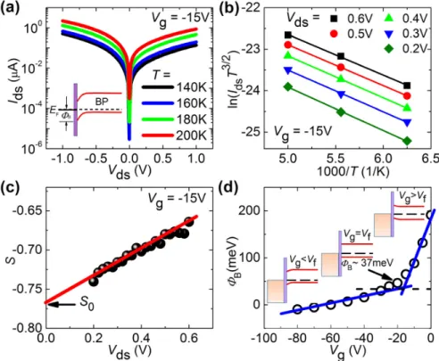
In order to extract the Schottky barrier height (UB) of
Au/Co/MgO contact on BP [inset of Fig.3(a)] and under-stand the effect ofVgonUB, we have measured theIds–Vds
characteristics with different Vg from 140 K to 200 K [Fig. 3(a)]. In this temperature range, the thermionic emission transport mechanism through the Schottky barrier can be mainly considered. We have employed a two-dimensional
thermionic emission equation describing the electrical trans-port through the Schottky barrier into the BP channel,35
Ids¼ AA)T1:5exp " q kBT UB" Vds n0 ! " # $ ; (2) whereA is the contact area, A* is the Richardson constant, q is the hole charge, andn0is the ideality factor. Figure3(b)shows
the Arrhenius plot [ln(Ids/T"3/2) vs. 1000/T] for different Vds.
The slopesS(Vds) extracted from the Arrhenius plot follow a
lin-ear dependence withVds:S(Vds)¼ "(q/1000kB)(UB"Vds/n0), as
displayed in Fig.3(c). Then the Schottky barrier height can be evaluated from the extrapolated value at zero Vds [S0
¼ "(qUB/1000kB)]. A similar procedure has been used to
determineUBwith differentVg, as shown in Fig.3(d).
As shown in the inset of Fig.3(d), the back-gate mainly plays two roles. One is to modulate the Fermi level inside the BP bandgap yielding a change of the carrier density in the channel. The second role is to modify the Schottky bar-rier profile and depletion layer width. In Fig.3(d), we can identify two regions from the variation of UB vs. Vg. For
Vg>"15 V when the depletion layer is thick, the thermionic
emission dominates, and this results in a large linear increase ofUBat lowjVgj. Note here, the UBobtained atVg¼ 0 V is
!200 meV, which is in good agreement with the value of 270 meV estimated from Ion/Ioff ratio at Vg¼ 0 V. For
Vg<"15 V, the tunneling current through the thin Schottky
barrier impinges on the linearity ofUB. The real value ofUB
for Co/MgO on BP is obtained at the point of the onset of the deviation (Vf¼ "15 V) equaling thus 37 meV, which is
cor-responding to the flat band condition. ThisUBvalue is much
smaller than the recent reports of Py contacts (110–200 meV),36 Au/Ti/BP contacts (200 meV),18 and Co/TiO
2/contacts
FIG. 3. (a)Ids" Vdscharacteristics for
temperatures between 140 and 200 K under Vg¼ "15 V. Inset: Schematics
of the Schottky barrier height for Co/ MgO contact onp-type BP. (b) ln(Ids/
T3/2
)versus 1000/T at different drain-source bias (Vds), in an Arrhenius plot
with linear fits in the temperature range from 160 K to 200 K. (c) Bias depen-dence of the slope (S) from linear fits. The slope at zeroVds (S0) is used to
extract the Schottky barrier heightUB.
(d) Schottky barrier height UB
extracted at different back-gate vol-tages. The real UB(37 meV) for Au/
Co/MgO on BP is obtained with the flat band condition (Vg¼ Vf¼ "15 V),
which is defined at the cross point from the linear response ofUBwithVg
(blue solid lines). Insert: band diagram of Co/MgO/BP interfaces with differ-ent back-gate voltages.
(50 meV).24The efficient lowingUBby inserting thin tunnel
barrier between the ferromagnetic metal and 2D materials have also been reported in TMDs systems.25,37,38This result of low Schottky barrier by using Au/Co/MgO tunneling con-tact is important for future application of BP based FET and spintronics.
F. Modulation of band structure by back-gate voltage In the end, to have a global view of the band structure modulation by the back-gate voltage, we have measuredIds
vs. Vdswith applying differentVgat 140 K. Figures4(a)and 4(b)showIds" Vdscharacteristics with negative and positive
Vg, respectively. From the analysis of UB vs. Vg, we have
identified that the flat band condition reaches atVg¼ "15 V
[Fig.3(d)]. In addition, due to the hole transport feature, the band structure can be schematically drawn as in Fig.4(d)with a situation of EC " EF > EF " EV. For Vg< "15 V, the
depletion layer tilts the band down due to theEFpinning at
the interface [Fig. 4(c)]. With the increase of negative Vg,
more hole can be injected into BP by crossing the depletion layer. ForVg>"15 V, the depletion layer tilts the band up at
the interface. However, it is not the case that the largerVgresults
in largerIds. From Fig.4(b), we can see that when we increase
Vgfrom 0 toþ80 V, the Idsfirstly decreases to a minimum at
Vg¼ þ10 V and then increases with Vg. This indicates that it is
hard to inject both holes and electrons atVg¼ þ10 V, which
should correspond to the condition thatEFis located in the
mid-dle of band (EC" EF¼ EF" EV), as shown in Fig.4(f). When
continuing with the increasingVg, both theEFmoving closer to
ECand the width of depletion region becoming thinner make
the conditions favorable for the electron injection into the BP
conduction band [Fig.4(g)]. Finally, at zero back-gate voltage, the BP shows a hole transport behavior (EC" EF> EF" EV),
while the depletion layer tilts up [Fig. 4(e)]. This could be related to the defects in the contact regions, which effectively pin the Fermi level at MgO/BP interface.
IV. CONCLUSION
In summary, we have studied the electrical transport properties in multilayer BP based FET device with Au/Co/ MgO tunneling contacts. In the hole dominated transport region, we have measured a minimum of Schottky barrier height of 37 meV for Au/Co/MgO contact on BP. Moreover, the transistor ON/OFF (Ion/Ioff) ratio is obtained as large as
107at 20 K and 105at 300 K. A systematic study of the tem-perature and back-gate voltage dependent conduction meas-urements has been performed to understand the modulation of the band structure and the ambipolar behavior. This dem-onstration of high ON/OFF ratio and low Schottky barrier height by using Au/Co/MgO tunneling contacts reveal a great potential promising for spintronics applications with multilayer black phosphorus field effect transistor.
ACKNOWLEDGMENTS
This work was supported by the French National Research Agency (ANR) MoS2ValleyControl project (Grant No. ANR-14-CE26-0017-04) and the joint ANR-National Natural Science Foundation of China (NNSFC) ENSEMBLE project (Grant Nos. ANR-14-CE26-0028-01 and NNSFC 61411136001). This work was also supported partly by the French PIA project “Lorraine Universit!e d’Excellence”, reference No. ANR-15-IDEX-04-LUE. The experiments were
FIG. 4. Characteristics ofIds" Vdsat 140 K, measured under (a) different negative back-gate voltages and (b) different positive back-gate voltages. (c)–(g)
Band structure of Co/MgO/BP interface modulated under different back-gate voltages. (c)Vg<"15 V; (d) Vg¼ "15 V; (e) Vg¼ 0 V; (f) Vg¼ þ10 V; (g)
Vg>þ10 V.
performed using the equipment from the platform TUBE–Davm funded by FEDER (EU), ANR, the Region Lorraine, and Grand Nancy.
1S. Novoselov, A. K. Geim, S. V. Morozov, D. Jiang, Y. Zhang, S. V.
Dubonos, I. V. Grigorieva, and A. A. Firsov, “Electric field effect in atom-ically thin carbon films,”Science306, 666 (2004).
2
K. A. H. Castro Neto, F. Guinea, N. M. R. Peres, K. S. Novoselov, and A. K. Geim, “The electronic properties of graphene,”Rev. Mod. Phys.81, 109 (2009).
3G. Fiori, F. Bonaccorso, G. Iannaccone, T. Palacios, D. Neumaier, A.
Seabaugh, S. K. Banerjee, and L. Colombo, “Electronics based on two-dimensional materials,”Nat. Nanotechnol.9, 768 (2014).
4
K. F. Mak, C. Lee, J. Hone, J. Shan, and T. F. Heinz, “Atomically thin MoS2:
a new direct-gap semiconductor,”Phys. Rev. Lett.105, 136805 (2010).
5
M. Xu, T. Liang, M. Shi, and H. Chen, “Graphene-like two-dimensional materials,”Chem. Rev.113, 3766 (2013).
6D. Jariwala, V. K. Sangwan, L. J. Lauhon, T. J. Marks, and M. C. Hersam,
“Emerging device applications for semiconducting two-dimensional tran-sition metal dichalcogenides,”ACS Nano8, 1102 (2014).
7B. Radisavljevic, A. Radenovic, J. Brivio, V. Giacometti, and A. Kis,
“Single-layer MoS2transistors,”Nat. Nanotechnol.6, 147 (2011). 8D. Xiao, G. Liu, W. Feng, X. Xu, and W. Yao, “Coupled spin and valley
physics in monolayers of MoS2 and other group-VI dichalcogenides,” Phys. Rev. Lett.108, 196802 (2012).
9S. Liang, H. Yang, P. Renucci, B. Tao, P. Laczkowski, S. Mc-Murtry, G.
Wang, X. Marie, J. George, S. Petit-Watelot, A. Djeffal, S. Mangin, H. Jaffres, and Y. Lu, “Electrical spin injection and detection in molybdenum disulfide multilayer channel,”Nat. Commun.8, 14947 (2017).
10D. Pacil!e, J. C. Meyer, C¸. €O. Girit, and A. Zettl, “The two-dimensional
phase of boron nitride: Few-atomic-layer sheets and suspended mem-branes,”Appl. Phys. Lett.92, 133107 (2008).
11Q. H. Wang, K. Kalantar-Zadeh, A. Kis, J. N. Coleman, and M. S. Strano,
“Electronics and optoelectronics of two- dimensional transition metal dichalcogenides,”Nat. Nanotechnol.7, 699 (2012).
12K. Lee, R. Gatensby, N. McEvoy, T. Hallam, and G. S. Duesberg, “High
performance sensors based on molybdenum disulfide thin films,”Adv. Mater.25, 6699 (2013).
13M. Bernardi, M. Palummo, and J. C. Grossman, “Extraordinary sunlight
absorption and one nanometer thick photovoltaics using two-dimensional monolayer materials,”Nano Lett.13, 3664 (2013).
14R. Kurapati, K. Kostarelos, M. Prato, and A. Bianco, “Biomedical uses for
2D materials beyond graphene: Current advances and challenges ahead,”
Adv. Mater.28, 6052 (2016).
15X. Zhang, L. Hou, A. Ciesielski, and P. Samor#ı, “2D materials beyond
gra-phene for high-performance energy storage applications,”Adv. Energy Mater.6, 1600671 (2016).
16V. Tran, R. Soklaski, Y. Liang, and L. Yang, “Layer-controlled band gap
and anisotropic excitons in few-layer black phosphorus,”Phys. Rev. B89, 235319 (2014).
17H. Liu, A. T. Neal, Z. Zhu, Z. Luo, X. Xu, D. Tom!anek, and P. D. Ye,
“Phosphorene: An unexplored 2D semiconductor with a high hole mobi-lity,”ACS Nano8, 4033 (2014).
18L. Li, Y. Yu, G. Ye, Q. Ge, X. Ou, H. Wu, D. Feng, X. Chen, and Y.
Zhang, “Black phosphorus field-effect transistors,”Nat. Nanotechnol.9, 372 (2014).
19S. P. Koenig, R. A. Doganov, H. Schmidt, A. H. Castro Neto, and B.
€
Ozyilmaz, “Electric field effect in ultrathin black phosphorus,” Appl. Phys. Lett.104, 103106 (2014).
20F. Xia, H. Wang, and Y. Jia, “Rediscovering black phosphorus as an
aniso-tropic layered material for optoelectronics and electronics,”Nat. Commun.
5, 4458 (2014).
21M. Buscema, D. J. Groenendijk, S. I. Blanter, G. A. Steele, H. S. J. van der
Zant, and A. Castellanos-Gomez, “Fast and broadband photoresponse of few-layer black phosphorus field-effect transistors,”Nano Lett.14, 3347 (2014).
22A. Avsar, J. Y. Tan, M. Kurpas, M. Gmitra, K. Watanabe, T. Taniguchi, J.
Fabian, and B. €Ozyilmaz, “Gate-tunable black phosphorus spin valve with nanosecond spin lifetimes,”Nat. Phys.13, 888 (2017).
23Y. Du, H. Liu, Y. Deng, and P. D. Ye, “Device perspective for black
phos-phorus field-effect transistors: Contact resistance, ambipolar and scaling,”
ACS Nano8, 10035 (2014).
24M. V. Kamalakar, B. N. Madhushankar, A. Dankert, and S. P. Dash, “Low
Schottky barrier black phosphorus field-effect devices with ferromagnetic tunnel contacts,”Small11, 2209 (2015).
25J. Chen, P. M. Odenthal, A. G. Swartz, G. C. Floyd, H. Wen, K. Y. Luo,
and R. K. Kawakami, “Control of Schottky barriers in single layer MoS2
transistors with ferromagnetic contacts,”Nano Lett.13, 3106 (2013).
26S. M. Sze and K. K. Ng,Physics of Semiconductor Devices (Wiley, 2007). 27K. Kaasbjerg, K. S. Thygesen, and K. W. Jacobsen, “Phonon limited
mobility in n-type single-layer MoS2from first principles,”Phys. Rev. B
85, 115317 (2012).
28E. H. Hwang and S. Das Sarma, “Acoustic phonon scattering limited
car-rier mobility in two-dimensional extrinsic graphene,”Phys. Rev. B77, 115449 (2008).
29
E. Mariani, A. J. Pearce, and F. von Oppen, “Fictitious gauge fields in bilayer graphene,”Phys. Rev. B86, 165448 (2012).
30H. Ochoa, E. V. Castro, M. I. Katsnelson, and F. Guinea,
“Temperature-dependent resistivity in bilayer graphene due to flexural phonons,”Phys. Rev. B83, 235416 (2011).
31F. Xia, D. B. Farmer, Y. Lin, and P. Avouris, “Graphene field-effect
tran-sistors with high on/off current ratio and large transport band gap at room temperature,”Nano Lett.10, 715 (2010).
32
Y. Lu, M. Tran, H. Jaffre`s, P. Seneor, C. Deranlot, F. Petroff, J.-M. George, B. L!epine, S. Ababou, and G. J!ez!equel, “Spin-polarized inelastic tunneling through insulating barriers,” Phys. Rev. Lett. 102, 176801 (2009).
33
J. Appenzeller, M. Radosavljevic, J. Knoch, and P. Avouris, “Tunneling versus thermionic emission in one-dimensional semiconductors,” Phys. Rev. Lett.92, 048301 (2004).
34Z. Chen, Y. M. Lin, M. J. Rooks, and P. Avouris, “Graphene nano-ribbon
electronics,”Physica E40, 228 (2007).
35A. Anwar, B. Nabet, J. Culp, and F. Castro, “Effects of electron
confine-ment on thermionic emission current in a modulation doped hetero-structure,”J. Appl. Phys.85, 2663 (1999).
36
Y. Anugrah, M. C. Robbins, P. A. Crowell, and S. J. Koester, “Determination of the Schottky barrier height of ferromagnetic contacts to few-layer phosphorene,”Appl. Phys. Lett.106, 103108 (2015).
37W. Wang, Y. Liu, L. Tang, Y. Jin, T. Zhao, and F. Xiu, “Controllable
Schottky barriers between MoS2 and permalloy,” Sci. Rep. 4, 6928
(2014).
38A. Dankert, L. Langouche, M. V. Kamalakar, and S. P. Dash,
“High-per-formance molybdenum disulfide field-effect transistors with spin tunnel contacts,”ACS Nano8, 476–482 (2014).