HAL Id: hal-00737872
https://hal.archives-ouvertes.fr/hal-00737872
Submitted on 26 Jun 2018
HAL is a multi-disciplinary open access
archive for the deposit and dissemination of
sci-entific research documents, whether they are
pub-lished or not. The documents may come from
teaching and research institutions in France or
abroad, or from public or private research centers.
L’archive ouverte pluridisciplinaire HAL, est
destinée au dépôt et à la diffusion de documents
scientifiques de niveau recherche, publiés ou non,
émanant des établissements d’enseignement et de
recherche français ou étrangers, des laboratoires
publics ou privés.
Hafnium Silicate dielectrics fabricated by RF magnetron
sputtering.
L. Khomenkova, X. Portier, P. Marie, F. Gourbilleau
To cite this version:
L. Khomenkova, X. Portier, P. Marie, F. Gourbilleau. Hafnium Silicate dielectrics fabricated by
RF magnetron sputtering.. Journal of Non-Crystalline Solids, Elsevier, 2011, 357 (8-9), pp.1860.
�10.1016/j.jnoncrysol.2010.12.048�. �hal-00737872�
Hafnium silicate dielectrics fabricated by RF magnetron sputtering
L. Khomenkova
⁎
,1, X. Portier, P. Marie, F. Gourbilleau
CIMAP, CEA/CNRS/ENSICAEN/UCBN, 6 Boulevard du Maréchal-Juin, F-14050 Caen Cedex, France
a b s t r a c t
Keywords:
High-k dielectrics; Hafnium oxide; Hafnium silicate; RF magnetron sputtering;
Structural and composition properties of hafnium silicate layers fabricated by RF magnetron sputtering were studied by means of spectroscopic ellipsometry, X-ray diffraction, transmission electron microscopy and attenuated total reflection infrared spectroscopy with respect to the deposition parameters and post-deposition annealing treatment. The variation of the post-deposition conditions allows the temperature of amorphous-crystalline phase transformation of pure hafnium oxide layers to be controlled. It is shown that the silicon incorporation in oxide matrix prevents the formation of interfacial silicon oxide layer and plays a major role in the stability of the structure of hafnium based layers remaining an amorphous state upon annealing at 900–950 °C.
1. Introduction
High-k oxides are promising for future CMOS devices owing to wide band gap (higher than 5 eV), good thermal stability on silicon and high permittivity (more than 20), which are vital to overcome the problem of high leakage current [1–5]. Based on thermodynamic studies [6] and band gap measurements [7], hafnium oxide is considered as the best candidate among high-k dielectrics to replace silicon oxide and its oxynitride in CMOS devices. However, the microstructure, optic and electrical properties of ultrathin films depend strongly on the fabrication process, growth conditions and post deposition treatment.
The most widespread techniques for fabrication of ultrathin layers were ALD, CVD and MOCVD[5,8–11]. Unfortunately, lower-temperature methods such as physical vapor deposition[12]and magnetron sputtering
[13–16]were not often addressed. It is worth to note that magnetron sputtered HfO2layers were fabricated by sputtering of pure metallic Hf
cathode either in argon–oxygen gas mixture[13], or in pure argon plasma and then submitted to oxidation. Only in a few cases, the layers were deposited from a pure HfO2target[14–18].
The use of pure HfO2as a gate dielectric in the direct contact with
Si substrate suffered from the undesirable formation of an interfacial SiO2 layer during deposition or annealing treatment [1,2]. To
overcome this problem, it was proposed to form Si oxynitride or
nitride barrier between high-k material and the Si substrate. Another drawback of pure HfO2is its low crystallization temperature (about
350–500 °C) accompanied usually by a formation of monoclinic phase. At the same time, amorphousfilms are advantageous because of their lower leakage current, a better homogeneity and, moreover, a higher reproducibility for the electrical properties in comparison with polycrystalline gate dielectric films. The improvement of thermal stability of amorphous HfO2 phase was an issue of numerous
investigations. It was shown, for example, in Refs.[13,19]that the incorporation of nitrogen into high-k matrix either during the deposition or post-deposition processing allows amorphous HfON films to be thermally stable up to 1100 °C.
The dielectric properties of HfO2 depend significantly on its
microstructure: both amorphous and monoclinic phases exhibit a dielectric constant of 16–20, but cubic and tetragonal phases have higher relative permittivity (about 28[20]) and they are preferable in terms of device application. The formation of tetragonal and cubic phases requires an incorporation of cationic dopants in the HfO2matrix as it was
demonstrated both theoretically[21–23]and experimentally[24–26]. Note that the dopants have to be carefully chosen to prevent a significant decrease of the band gap energy and dielectric constant of the material. The most promising candidate to fulfill these conditions is silicon. Its incorporation into HfO2 matrix results in the formation of
pseudobinary alloys such as (HfO2)x(SiO2)1−x. A significant decrease
of leakage current and an improvement of thermodynamic stability of this alloy were demonstrated in Refs. [1–3,27]. However, the permittivity of this material depends significantly on its composition and in most cases it was found to be less than 10, whereas higher permittivity values are required for microelectronic applications. Considering the above mentioned discussion, the effect of the silicon
⁎ Corresponding author. Permanent address: V.Lashkaryov Institute of Semiconduc-tor Physics, NAS Ukraine, 45 Pr. Nauky, 03028 Kyiv, Ukraine. Tel.: +380 44 5257234.
E-mail addresses:[email protected],[email protected]
(L. Khomenkova),[email protected](F. Gourbilleau).
1
incorporation on the properties of HfSiO dielectric materials requires further investigation.
In the present study, HfO2-based thin layers have been fabricated by RF
magnetron sputtering of a pure HfO2or composed HfO2+Si targets in
pure argon plasma. The properties of the layers have been analyzed by means of X-ray diffraction, phase-modulated spectroscopic ellipsometry, infrared absorption spectroscopy and high resolution transmission electron microscopy with respect to the deposition conditions and the annealing treatments.
2. Experimental
The layers investigated were grown on B-doped (100) oriented Si substrates with a resistivity of 15Ω cm. The substrates were cleaned in a diluted hydrofluoric solution (10%) to remove native oxide, dried in nitrogenflow and immediately placed into the vacuum chamber of the deposition setup.
Pure and Si-rich HfO2layers were grown by RF magnetron sputtering
of 4 inches HfO2target (99.9%) in pure argon plasma at RF power density
RFP=0.74–1.2 W/cm2. The substrate temperature was kept at 45 and
100 °C, the total plasma pressure and substrate-cathode distance were fixed at 0.04 mbar and 57 mm, respectively. Si-rich layers were fabricated by the co-sputtering of HfO2target topped by Si chips with
a surface ratio of RSi=12%. The latter was estimated as a ratio of the
surface of all Si chips to the total surface of HfO2target. To study the
thermal stability of the layers, an annealing treatment in nitrogenflow in a conventional furnace at different temperatures TA= 600–1100 °C
during tA= 15 and 30 min was performed.
Several techniques were used to analyze the properties of the layers. The thickness of thefilms was analyzed by means of X-ray reflectometry and phase-modulated spectroscopic ellipsometry. Besides, the last technique was used to determine optical parameters of the films. The data were collected by means of a Jobin-Yvon ellipsometer (UVISEL) where the incident light was scanned in the range of 1.5–4.5 eV under an incident angle of 66.3°. The fitting of the experimental data was performed using DeltaPsi2 software[28]. The uncertainty of this method in the estimation of the refractive index is Δn=±0.01. ATR–FTIR technique was used to control the chemical composition of the layers. The spectra were measured in the range of 600–4000 cm−1by means of a 60° Ge Smart Ark accessory inserted in
a Nicolet Nexus spectrometer. X-ray diffraction analysis was performed using a Phillips XPERT HPD Pro device with a Cu Kα
radiation (λ=0.154 nm) at a fixed grazing angle incidence of 0.5°. Cross-sectional specimens were prepared for TEM examination by the standard procedure involving grinding, dimpling and Ar+ion beam
thinning until electron transparency. The samples were observed by conventional (CTEM) and high resolution electron microscopy (HRTEM) using a FEG 2010 JEOL instrument, operated at 200 kV. Image processing was done with the commercial Digital micrograph GATAN software.
3. Results
3.1. Spectroscopic ellipsometry analysis
Spectroscopic ellipsometry does not require special environment and can be easily integrated into a semiconductor processing[29,30]
as a fast, sensitive and non-destructive method forfilm characteriza-tion. The fitting of the experimental data is usually based on the effective medium approximation (EMA) [29,31]. There are several EMA models (Bruggeman, Maxwell-Garnet, etc.). As for all meanfield theories, they fail to predict the properties of a multiphase medium close to the percolation threshold due to its long-range correlation length. They suppose that the macroscopic system is homogeneous (with correlation length below the Lorentz cavity radius) whereas the properties of multiphase system are determined by the properties of
its components and their relative fractions. The most considered parameters are conductivity and/or dielectric constant.
In the present work, Bruggeman effective medium approximation (BEMA) is used[31]. To investigate the properties of the as-deposited and annealed layers, a four-phase optical model is applied [18]. It consists of a silicon substrate, an interfacial SiO2layer, an amorphous
HfO-based layer (pure or Si-rich), and a surface rough layer, composed of a mixture of void space and HfO2-based layer. To fit
spectroscopic ellipsometry data, the dispersion law for n and k was chosen as described in Ref.[18]. It is based on the Forouhi–Bloomer model elaborated for amorphous semiconductor and insulating materials[32]using an improved parameterization[33]. The model structure and optical properties of thefilms were optimized by least-square refinement approach (χ2) from afitting of the experimental
data. As a result, the thickness of HfO-basedfilm (pure or Si-rich) and interfacial SiO2 layer, the dispersion law of refractive index and
absorption coefficient were obtained.
The evolution of the refractive index of pure HfO2and HfSiOfilms
with the annealing treatment is presented inFig. 1. As one can see, as-deposited pure HfO2film demonstrates an n value around 2.03 at 2-eV
light energy. The annealing treatment shows a slight decrease of the refractive index down to n = 1.97 (Fig. 1a, curve 1). Using the Clausius–Mossotti relationship between optical dielectric constant and film density, ρ, the latter was estimated with the relative uncertainty of≤5%. As for pure HfO2films, they were considered to be
composed of HfO6and/or HfO8unit cells[20]and their density was
found to be in the range of 8.0–8.8 g/cm3. It increased slightly for
higher temperatures (Fig. 1b) confirming the data described in Ref.
[34].
The as-deposited HfSiO films exhibit the higher n value in comparison with pure HfO2 films, i.e. 2.12 against 2.03 (Fig. 1a)
whereas n decreases upon annealing (Fig. 1a). Thus, HfSiO films annealed at TA≥800 °C exhibit lower n values (n=1.85) than their
pure counterparts (n = 1.97). Besides, they demonstrate the decrease of the extinction coefficient, k, followed by a shift of the “absorption
a)
b)
Fig. 1. The evolution of (a) the refractive index, n, and (b) the density of the films, ρ, with annealing temperature for pure HfO2and HfSiOfilms. The annealing time is
15 min. The density of the HfO2films is estimated for two unit cells as HfO6and HfO8,
the density of HfSiOfilms is presented considering two possible unit cells as HfO6/SiO4
and HfO8/SiO4.
edge” to higher energy side (not shown here). Since the optic model, proposed in the present study, allows the contributions of interfacial SiO2 layer and HfO-based layer to be separated, this means that a
decrease of n and k values observed for HfSiO upon annealing is more likely due to structural transformation of HfO-based layer itself rather than due to the increase of the contribution of interfacial SiO2one. In
the case of pure HfO2films, the formation of voids in film volume can
explain the decrease of the refractive index. It could be the same reason for the n evolution in the case of HfSiO films, but the formation of SiO2phase stimulated by high temperature annealing has also to be
taken into account as a cause of the refractive index decrease. Moreover, as we showed earlier[16,17], an annealing at TA= 800 °C
for 15 min did not lead to the formation of any pores in the HfSiO volume. Consequently a formation of SiO2phase could be only the
reason of the lowering of the refractive index upon annealing and this can explain the increasing offilm transparency.
The density of the HfSiOfilms was also estimated based on the approach described in Ref.[18]. Similar to the case of pure HfO2films
it was assumed that the HfO2phase is presented by HfO6and/or HfO8
unit cells, whereas the SiO2phase consisted of SiO4unit cells. The
results obtained, considering both possibilities, are presented in
Fig. 1b. Thefilm density decreases gradually from 7.3–7.8 g/cm3
down to 5.9–6.3 g/cm3. This can be explained by the SiO
2phase formation
for thefilms annealed at TA≤800 °C. However, annealing at higher
temperatures could also cause pores formation. To discriminate the origin of the variation of thefilm density with annealing treatment, analyses of the chemical composition and structure of thefilms were made by ATR and XRD methods, whereas TEM study was performed to obtain information about the microstructure of thefilms. 3.2. ATR infrared spectra of the films
Among the nondestructive methods used to study thinfilms, ATR technique holds an important place, since it allows very thin layers to be analyzed. Unfortunately, referenced ATR data for HfSiO materials are not so numerous. The only known data are those regarding the monoclinic HfO2 phase, while for tetragonal and cubic phases of HfO2 and,
moreover, for HfSiO4they are not available in the case of thinfilms.
The interpretation of experimental data obtained for high-k silicate materials is usually based on the comparison of infrared spectra obtained for amorphous SiO2and HfO2, and their transformation due
to an increase of the high-k material contribution. Information about the crystalline or amorphous nature of the layers can be extracted from the peak shape and the position of the band(s). Usually, Hf–O vibration bands are located in the range of 600–800 cm−1[36,37].
When crystalline HfO2 phase is present in the layer, the
well-defined peaks are detected at 770–780 cm−1and 675–685 cm−1, the
first peak being the signature of the monoclinic HfO2phase[36,37].
The observation of only one broad band with a maximum around 690–700 cm−1was usually attributed to the amorphous nature of the
layers[16,17,36].
ATR experiments have been performed on the same pure and Si-rich layers described above. The presence of two main vibration bands in the range of 600–800 cm−1and 960–1260 cm−1was revealed for pure HfO
2
layers (Fig. 2). The first band corresponds to the Hf–O vibrations, whereas the second one is due to Si–O vibrations. Its presence is caused by a SiOxinterfacial layer[1,2,4,8,16,17], whereas the shape and peak
position depend on its thickness and composition[37].
It is known that continuous random network of SiO2 consists of
corner-coordinated SiO4 tetrahedra and a disorder of amorphous
structures comes from the changes of Si–O–Si bond angle. Usually, SiO2leads to four main peaks in the mid-infrared range coming mainly
from motion of oxygen atoms. Under specific conditions several LO and TO phonons of Si–O bond can be detected in the 450–1350 cm−1
spectral range: at 1076 cm−1(TO3) and 1256 cm−1(LO3), at 1160 cm−1
(TO4) and 1200 cm−1(LO4), at 810 cm−1(TO2) and 820 cm (LO2) as
well as at 457 cm–1(TO1)–507 cm−1(LO1)[38,39]. The decrease of SiO2
layer thickness to a nanometer scale is accompanied by a shift of the peak positions of all vibration bands to lower wavenumbers as well as by a decrease of the intensity of TO4–LO4 phonons that are usually
considered as a feature of the disordering of SiO2matrix[39]. In the case
of LO3and TO3phonons, this shift is about 25–30 cm−1[40]. However,
the detection of LO3phonon is usually considered as an evidence of the
formation of perfect Si/SiO2interface[41]and the spectral shift of LO3
and TO3 peak positions towards higher wavenumbers confirms the
formation of a stoichiometric silicon oxide layer and increase of its thickness[17,37].
Annealing treatment of pure HfO2layers results in the different
behaviours of Si–O and Hf–O vibration bands. Thus, initial broad Si–O band, centred at about 1100 cm−1(Fig. 2), shifts towards 1180 cm−1 when TA= 800 °C accompanied by an appearance of well-defined LO3
and TO3phonon modes. Upon TAincrease, it results in a shift of both of
them towards 1230 cm−1and 1070 cm−1, respectively. This is due to the formation of stoichiometric SiO2 interfacial layer caused by a
diffusion of oxygen towards the film/substrate interface. This diffusion is usually considered as a diffusion of the oxygen from environment through the whole volume of high-k layer. However, it was shown for the case of sputtered layers[35], it occurs preferably from the HfO2 layer close to HfO2/Si interface. Since the films
investigated were annealed in nitrogen atmosphere, the layer closed to HfO2/Si interface could be enriched by hafnium caused the
formation of oxygen deficient centres. The composition of as-deposited and annealed at TA=800 °C layers by energyfiltered TEM
analysis gave the evidence that HfO2 layer is stoichiometric (not
shown here). However, the formation of oxygen-deficient centres
Fig. 2. ATR spectra of as-deposited (AD) and annealed at different temperatures HfO2
(solid lines) and HfSiO (dashed lines) samples. Annealing temperatures are mentioned in thefigure, annealing time is 15 min.
should occur at higher annealing temperatures due to the formation of monoclinic HfO2grains observed by ATR investigation. As one can
see from Fig. 2, the evolution of the Hf–O vibration band is accompanied by the presence of a shoulder at about 770 cm−1 transformed to a well-defined band at higher temperatures. Two separate bands at 770 cm−1and 680 cm−1detected for the layers annealed at 1100 °C confirm the appearance of monoclinic HfO2
phase.
The ATR spectra of as-deposited HfSiOfilms demonstrate featureless broad band peaked at 1050 cm−1with a shoulder at about 900 cm−1 and a tail up to 600 cm−1(Fig. 2). This is the evidence of the formation of a HfSiO matrix. An annealing of the layers at TA= 800 °C for 15 min leads
to the increase of the intensity as well as to the slight narrowing and to the shift of the broad ATR peak from 1050 cm−1to 1070 cm−1. On the contrary to pure HfO2layers, the lower wavenumber part of the ATR
spectrum does not change and is still featureless (Fig. 2). Further increase of the temperature up to TA= 900–1000 °C results in the
continuous increase of the peak intensity, shift of the peak position to 1120 cm−1and the appearance of a shoulder at about 1220 cm−1. A treatment at TA= 1100 °C causes the narrowing of this vibration band, a
redistribution of the intensities of its components and an appearance of the band at about 820 cm−1. All these three bands are ascribed to the SiO2phase[18]. The formation of an interfacial SiO2layer is confirmed
by the well-defined LO3phonon whose intensity exceeds the TO3one
(Fig. 2). At the same time, a comparable contribution of TO3and TO4–LO4
phonons to ATR spectrum enables us to assume that the increase of the thickness of interfacial SiO2layers as well as the formation of SiO2phase
inside thefilm volume is more likely due to the phase separation of the HfSiO film on SiO2 and HfO2phases. The latter is confirmed by an
increase of the Hf–O vibrations' intensity in the range of 600–780 cm−1
at TA≥1000 °C. This broad and featureless band is usually ascribed to
amorphous HfO2[11,12]. However, it is hardly believable that such high
annealing temperature (1100 °C) would lead to an amorphous HfO2
phase.
To get more information about the structure of HfO2phase, we
performed a XRD study of these samples. It is worth to note that the similarity of the ATR spectra obtained for as-deposited and annealed at TA≤900 °C testifies the thermal stability of the HfSiO layers. The
most probable reason explaining this phenomenon is the high flexibility of Si–O bonds that allows the amorphous nature of the materials to be kept (similar, for example, to fused silica). However, although HfSiO can be stable at such annealing temperatures, the slight transformation of Si–O vibration band can be due to the formation of a SiO2interfacial layer. The latter could occur at lower
temperatures (less than 900 °C) than that corresponding to the phase separation in HfSiO film (1000–1100 °C). To clarify this issue, we performed TEM observations of cross-sections of the samples that will be presented below after the analysis of XRD data.
4. Discussion
4.1. XRD study of pure HfO2and HfSiO layers
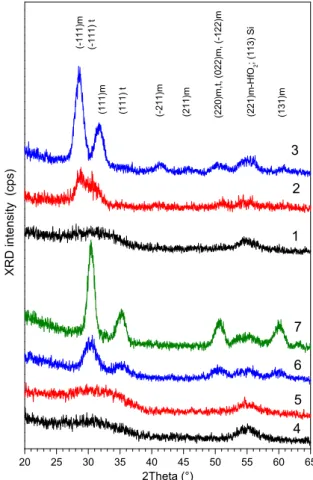
It is known that XRD patterns, obtained in asymmetric grazing geometry, allow studying the distribution of structural properties across thin layers. The monoclinic HfO2phase is usually revealed in
XRD patterns by the most intense peaks in the range of 2θ=15–65° at 2θ=28.37° and 31.67° (for (111) planes), 2θ=34.34°, 34.66° and 35.55° (for (200) planes), and 2θ=49.59°, 50.49° and 50.91° (for (220) planes)[42]. The decrease of HfO2 grain sizes results in the
broadening of XRD peaks and for the case of amorphous structure only one broad peak in the range of 2θ=28–32° is usually observed
[14,15].
The as-deposited pure HfO2and HfSiOfilms show a broad peak in
the range of 2θ=25–35° with a maximum intensity at about 2θ=32° (Fig. 3), which is consistent with the amorphous nature of both pure
and Si-richfilms. The annealing of pure HfO2film at 800 °C results in
the transformation of the shape of broad XRD peak and an appearance of two overlapped peaks at 2θ=28.5° and 2θ=31.7°, that can be considered as a formation of monoclinic phase. This annealing does not lead to the crystallization of HfSiOfilms. At higher TA, a formation
of the HfO2monoclinic phase is evident by an increase of the observed
peaks' intensity with their concomitant narrowing and an appearance of some peaks in the range of 2θ=40–65° (Fig. 3). Annealing of HfSiO film at 1100 °C results in the appearance of the peaks at 2θ=30.3°, 2θ=35.3° and 2θ=50.6°, that become to be more pronounced for longer annealing time. These peaks can be ascribed to the (111), (200) and (220) crystalline planes of the tetragonal HfO2phase. The peak at
2θ=59.8° can be considered as an overlapping of the reflections from (311) and (222) planes of the same phase.
Usually, tetragonal HfO2phase is observed for ultrathinfilms, but
annealing treatment at temperatures as high as 800 °C favors its transformation to monoclinic one[43]. However, in our case, longer annealing treatment (up to 30 min) at 1100 °C results in the increasing of the intensities of observed XRD peaks only and does not lead to an appearance of other peaks. This can be an evidence of thermal stability of the tetragonal HfO2phase in our samples. Since it
has higher dielectric constant in comparison with that of monoclinic one, such afilm can be used as a gate material for the structures that need high-temperature annealing process such as some nanomemory structures with embedded Si nanoparticles[44].
The analysis of optical properties of the HfSiO layers showed a decrease of their refractive index with annealing treatment. Regarding the structural properties, the phase separation is confirmed by the ATR spectra, whereas the crystallization of HfO2phase is demonstrated by
the XRD data. Since an increase of n is expected with the HfO2
Fig. 3. XRD patterns measured for pure HfO2(1–3) and HfSiO (4–7) layers: as-deposited
(1, 4) and annealed at TA= 800 °C (2, 5) and 1100 °C (3, 6, 7) for 15 min (1–6) and
30 min (7).
crystallization, we concluded that the refractive index of HfSiOfilms decreases continuously due to an increasing contribution of the SiO2
phase. At the same time, neither ATR nor XRD studies can reveal unambiguously where the SiO2phase is located, i.e. atfilm/substrate
interface or embedded in thefilm volume. However, based on these results and on the estimate of the film density, we can admit the presence of SiO2phase inside the volume of HfSiO layer. The latter will
be confirmed by TEM observations of as-deposited and annealed films. 4.2. TEM observation
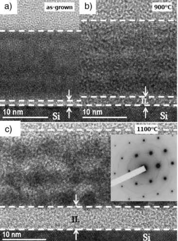
TEM images of cross-sections of as-deposited and annealed samples are shown inFig. 4a. As-deposited samples are homogeneous, smooth enough (roughness does not exceed 1 nm) and do not have thick interfacial layer (the thickness being lower than 1 nm). These observations corroborate the results obtained by fitting of ellipso-metry spectra. The increase of the annealing temperature up to 900 °C leads to the increase of totalfilm thickness. However, this occurs not only due to the increase of the interfacial SiO2layer thickness, but also
due to the expansion of HfSiOfilm itself (Fig. 4b). The appearance of bright and dark alternated lines parallel to thefilm/substrate interface is seen. This can be explained by the Hf segregation process, whereas thefilm remains amorphous (Fig. 4b).
Further increase of annealing temperature up to 1100 °C results in the formation of a thicker SiO2interfacial layer (up to 5 nm) as well as
a higher contrast between bright and dark regions (Fig. 4b,c). They correspond to SiO2-rich and HfO2-rich phases that are an evidence of
the HfSiO phase separation. Besides, the crystallites appear in the dark regions as demonstrated byFig. 4c. The formation and crystallization
of HfO2phase usually leads to the increase of thefilm density. At the
same time the appearance of SiO2phase results in the decrease of the
film density and can be considered as a main reason of the decrease of the total density of the HfSiOfilm upon annealing.
It is known that thick pure HfO2has usually the monoclinic phase,
whereas tetragonal and cubic phases appear at 1670–2200 °C[35]. When the layer thickness decreases down to a nanometer scale, the presence of the tetragonal phase can be observed in pure HfO2layers
[36]. However, it transforms easily to the monoclinic one at moderate temperatures[36]. The analysis of crystallized HfO2phase of HfSiO
films was also performed. The inset in Fig. 4c presents a typical selected area electron diffraction (SAED) pattern corresponding to the film and a part of the [110] oriented silicon substrate. Apart from the well defined dots, rising from the silicon substrate, four weak rings appeared. The lattice plane distances estimated from SAED were 2.95 Å, 1.80 Å and 1.53 Å. These distances are compatible with lattice planes of the HfO2tetragonal phase: d[111]= 2.95 Å, d[220]= 1.82 Å.
and d[311]= 1.59 Å. Thus, TEM observations of HfSiOfilms show that
the tetragonal phase is stable in suchfilms upon annealing at 1100 °C, confirming the XRD study.
5. Conclusion
The effect of annealing treatment on the properties of HfO2-based
layers has been investigated. It is demonstrated that silicon incorporation into the HfO2matrix leads to a decrease in the thickness of interfacial layer
down to 1 nm and improves the thermal stability of the layers upon annealing at 900–950 °C. The film density was estimated with respect to annealing temperature. Its decrease with temperature is explained by a phase separation of HfSiO on HfO2and SiO2phases over its volume and the
increase of the contribution of the latter with annealing. The formation of the HfO2tetragonal phase was also revealed. The latter was found to be
stable offering a possibility to use such HfSiO materials for microelectronic applications, for example, for nanomemory structures with embedded Si nanoparticles requiring high-temperature annealing. The formation of the Si-rich/Hf-rich multilayer structure upon annealing treatment was observed.
Acknowledgments
This work is supported by the French National Research Agency (ANR) through Nanoscience and Nanotechnology Program (NOMAD Project n°ANR-07-NANO-022-02) and by the Conseil Régional de Basse Normandie through the CPER project— Nanoscience axe (2007–2013). References
[1] G.D. Wilk, R.M. Wallace, J.M. Anthony, J. Appl. Phys. 87 (2000) 484. [2] G.D. Wilk, R.M. Wallace, J.M. Anthony, J. Appl. Phys. 89 (2001) 5243. [3] C. Krug, G. Lucovsky, J. Vac. Sci. Technol. A. 22 (2004) 1301.
[4] M. Houssa, L. Pantisano, R. Degraeve, T. Schram, G. Pourtois, S. De Gendt, G. Groeseneken, M.M. Heyns, Mat. Sci. Eng. R 51 (2006) 37.
[5] G. Pant, A. Gnade, M.J. Kim, R.M. Wallace, B.E. Gnade, M.A. Quevedo-Lopez, P.D. Kirsch, A. Gnade, S. Krishnan, Appl. Phys. Lett. 89 (2006) 032904.
[6] M. Gutowski, J.E. Jaffe, Ch.-L. Liu, M. Stoker, R.I. Hegde, R.S. Rai, P.J. Tobin, Appl. Phys. Lett. 80 (2002) 1897.
[7] H. Kato, T. Nango, T. Miyagawa, T. Katagiri, K.S. Seol, Y. Ohki, Appl. Phys. Lett. 92 (2002) 1106.
[8] J.-H. Kim, V.A. Ignatova, M. Weisheit, Microelectron. Eng. 86 (2009) 357. [9] S.K. Dey, A. Das, M. Tsai, D. Gu, M. Flyod, R.W. Carpenter, H. De Waard, C.
Werkhoven, S. Marcus, J. Appl. Phys. 95 (2004) 5042.
[10] B.K. Park, J. Park, M. Cho, C.S. Hwang, K. Oh, Y. Han, D.Y. Yang, Appl. Phys. Lett. 80 (2002) 2368.
[11] M. Lui, L.Q. Zhu, G. He, Z.M. Wang, J.X. Wu, J.-Y. Zhang, I. Liaw, Q. Fang, I.W. Boyd, Appl. Surf. Sci. 253 (2007) 7869.
[12] K. Yamamoto, S. Hayashi, M. Kubota, M. Niwa, Appl. Phys. Lett. 81 (2002) 2053. [13] G. He, Q. Fang, L.D. Zang, Mat. Sci. Semicond. Proc. 9 (2006) 870.
[14] L. Pereira, A. Marques, H. Águas, N. Nedev, S. Georgiev, E. Fortunato, R. Martins, Mat. Sci. Eng. B 109 (2004) 89.
[15] L.-P. Feng, Z.-T. Liu, Y.-M. Shen, Vacuum 83 (2009) 902.
[16] L. Khomenkova, C. Dufour, P.-E. Coulon, C. Bonafos, F. Gourbilleau, Mater. Res. Soc. Symp. Proc. 1160 (2009) 69–72.
Fig. 4. TEM cross-sections of HfSiO layer taken for as-deposited (a), annealed at 900 °C (b) and 1100 °C (c) in nitrogenflow for 15 min. Electron diffraction pattern is shown for the sample annealed at 1100 °C. IL is interfacial SiO2layer.
[17] L. Khomenkova, C. Dufour, P.-E. Coulon, C. Bonafos, F. Gourbilleau, Nanotechnology 21 (2010) 095704.
[18] L. Khomenkova, J. Cardin, X. Portier, F. Gourbilleau, Nanotechnology 21 (2010) 285707.
[19] M.R. Visokay, J.J. Chambers, A.L.P. Rotondaro, A. Shanware, Appl. Phys. Lett. 80 (2002) 3183.
[20] G.-M. Rignanese, J. Phys. Condens. Matter 17 (2005) R357. [21] D. Fischer, A. Kersch, Appl. Phys. Lett. 92 (2008) 012908.
[22] Ch.-K. Lee, E. Cho, H.-S. Lee, Ch.S. Hwang, S. Han, J. Phys. Condens. Matter 78 (2008) 012102.
[23] E. Cockayne, J. Appl. Phys. 103 (2008) 084103.
[24] D. Tsoutsou, G. Apostolopoulos, S.F. Galata, P. Tsipas, A. Sotiropoulos, G. Mavrou, Y. Panayiotatos, A. Dimoulas, A. Lagoyannis, A.G. Karydas, V. Kantarelou, S. Harissopoulos, J. Appl. Phys. 106 (2009) 024107.
[25] P. Majumder, G. Jursich, C. Takoudis, J. Appl. Phys. 105 (2009) 104106. [26] K. Tomida, K. Kita, A. Turiumi, Appl. Phys. Lett. 89 (2006) 142902. [27] R. Beyers, J. Appl. Phys. 56 (1984) 147.
[28] http://www.horiba.com/scientific/products/ellipsometers/software/. [29] S. Charvet, R. Madelon, F. Gourbilleau, R. Rizk, J. Appl. Phys. 85 (1999) 4032.
[30] O. Buiu, W. Davey, Y. Lu, I.Z. Mitorvic, S. Hall, Thin Solid Films 517 (2008) 453. [31] D.A.G. Bruggeman, Ann. Phys. 416 (1935) 636.
[32] A.R. Forouhi, I. Bloomer, Phys. Rev. B 34 (1986) 7018. [33] G.E. Jelisson Jr., F.A. Modine, Appl. Phys. Lett. 69 (1996) 371. [34] T. Tan, Zh. Liu, H. Lu, W. Liu, H. Tian, Opt. Mater. 32 (2010) 432. [35] R. Jiang, E.Q. Xie, Z.F. Wang, J. Mater. Sci. 42 (2007) 7343.
[36] N.V. Nguyen, A.V. Davydov, D. Chandler-Horowitz, M.F. Frank, Appl. Phys. Lett. 87 (2005) 192903.
[37] M.M. Frank, S. Sayan, S. Dörmann, T.J. Emge, L.S. Wielunski, E. Garfunkel, Y.J. Chabal, Mat. Sci. Eng. B 109 (2004) 6.
[38] C.T. Kirk, Phys. Rev. B 38 (1988) 1255. [39] P. Lange, J. Appl. Phys. 66 (1989) 201.
[40] H. Ono, T. Ikarashi, K. Ando, T. Kitano, J. Appl. Phys. 84 (1998) 6064. [41] J.E. Olsen, F. Shimura, J. Appl. Phys. 66 (1989) 1353.
[42] JCPDS No.78-0050.
[43] J. Tang, F. Zhang, P. Zoogman, J. Fabbri, S.-W. Chan, P. Zhu, L.E. Brus, M.L. Steigerwald, Adv. Funct. Mater. 15 (2005) 1595.
[44] M. Perego, G. Seguini, C. Wiemer, M. Fanciulli, P.-E. Coulon, C. Bonafos, Nanotechnology 21 (2010) 055606.