Data-Driven Approach to Understanding
Exciton-Exciton Interactions in CsPbBr
3
Nanocrystals
MASSACHUSETTS INSTI
OF TECHNOLOGY
byMatthew N. Ashner
LIBRARIES
I
Bachelor of Science in Chemical Engineering Washington University in St. Louis, 2013 Master of Science in Chemical Engineering Practice
Massachusetts Institute of Technology, 2015
Submitted to the Department of Chemical Engineering on May 7th, 2019 in
the requirements for the degree of
ARCHIVES
partial fulfillment of
Doctor of Philosophy in Chemical Engineering at the
Massachusetts Institute of Technology
December 2019
D 2019 Massachusetts Institute of Technology.Signature of Author:
_Signature
redacted
Department of Chemical EngineeringMay 7th 2019
Sianature redacted
Certified by:
William A. Tisdale
ARCO Career Development Professor in Energy Studies
Thesis Supervisor
All rights reserved.
---- I--I--I
Accepted by: Patrick S. Doyle
Robert T. Haslam (1911) Professor of Chemical Engineering Chairman, Committee for Graduate Students
Signature
redacted
Data-Driven Approach to Understanding
Exciton-Exciton Interactions in CsPbBr
3
Nanocrystals
by
Matthew N. Ashner
Submitted to the Department of Chemical Engineering on May 7th, 2019 in partial fulfillment of
the requirements for the degree of Doctor of Philosophy in Chemical Engineering
Abstract
Lead halide perovskites are a rapidly developing class of materials of interest for optoelectronic applications. They have a number of desirable properties such as long carrier diffusion lengths and defect tolerance that arise from the materials' unique dielectric properties. Although much of the initial interest in lead halide perovskites was geared towards producing highly efficient solar cells from the bulk material, cubic perovskite nanocrystals are a strong candidate system for light-emitting applications. Optical gain in semiconductor nanocrystals relies on emission from biexciton or doubly excited states. Knowledge of the spectral properties of biexciton states is critical for understanding optical gain development as well as many-body interactions
between charge carriers more broadly.
In this thesis, we develop and demonstrate a data-driven approach to characterizing the energetics and dynamics of biexciton states in CsPbBr3 nanocrystals using TA spectroscopy. We then use the understanding developed using the TA data to guide experiments using other techniques and further examine the physical phenomena that influence these excited states. In Chapter 2, we describe our data-driven method in detail and demonstrate its effectiveness in extracting spectral information about CsPbBr3 nanocrystals. The method combines the target analysis fit commonly employed in organic systems with Bayesian inference and a Markov chain Monte Carlo sampler to accurately characterize the model uncertainty and vet the model itself. In Chapter 3, we apply the analysis developed in Chapter 2 to a size-series of CsPbBr3
nanocrystal size. We find that the exciton and biexciton spectra have distinctive shapes, in
contrast with the common assumption about these spectra. The biexciton spectra a broader
and slightly blue-shifted from the exciton spectrum, and the broadening and blue-shifting both
increase as the nanocrystal size decreases. We verify this with our own time-resolved
photoluminescence experiments. In Chapter 4, we propose and discuss in detail the
development of an experiment to verify our hypothesis for why the exciton-exciton interaction
is repulsive - the effect of polaron formation. We describe the development of a femtosecond
stimulated Raman spectroscopy experiment to directly observe polaron formation and the
challenges of performing this technique at high repetition rate. The central goal of this thesis is
to describe a more careful approach to analyzing spectroscopic data.
Thesis Supervisor: William A. Tisdale
Title: ARCO Career Development Professor in Energy Studies
Acknowledgements
There are numerous people I would like to thank for making this thesis and my success at MIT possible. I would like to begin by thanking my sources of funding: The National Defense Science and Engineering Graduate Fellowship, The National Science Foundation, and The Department of Energy via the MIT-Harvard Center for Excitonics.
First and foremost, I am beyond grateful to my PhD advisor, Will Tisdale, for making my
graduate school experience so positive and fostering my professional growth as a scientist and engineer. From the very beginning, Will believed in me more than I believed in myself and gave me the confidence to dive into trust in the work I was doing. Along the way he provided
constant mentorship and technical guidance while being a fun and engaging person to work with on a personal level. Will also took great care to create a positive and supportive work environment in the lab as a whole that shaped my time in graduate school.
I would like to thank my thesis committee, Michael Strano and Gabriela Schlau-Cohen for providing me with guidance at critical junctures during my PhD. Michael always helped me keep a birds-eye view of what my thesis could be, and Gabriela gave me much advice on several key technical points throughout the process that made for a stronger body of work.
From the Tisdale Lab, I would like to begin by thanking Katie Shulenberger for being the best collaborator and data buddy I could have ever asked for. Much of the work in this thesis began with her approaching me with these materials and a problem to solve. This led to an amazing collaboration far greater than the sum of its parts, and the basis of Chapter 3 is published as co-first authored papers with Katie as a result. Many thanks to Katie for being my guide to photon counting and the nanocrystal literature, for the countless hours of brainstorming, for always being a listening ear and source of moral support throughout this process, and of course for technical contributions to this work. I would also like to thank Sam Winslow for bringing the MCMC tool to my attention and helping with the implementation as this work would not have been possible without it. Many thanks to Rachel Gilmore and Aaron Goodman for teaching me
so much about optics and ultrafast spectroscopy in my early days. In addition to Rachel and Aaron, I would like to extend a thank you to Dan Congreve and Yunan Gao being sources of advice, perspective and support when I needed it most. I would like to thank Eric Powers for being a pleasure to work with as a mentee and always offering to lend a hand with data collection through the course of his training. Many thanks to Barb Balkwill for her help with many logistical needs and for being an endless source of moral support. Finally, I would like to thank each and every member of the Tisdale Lab for being such great colleagues and for making
our group what it is - Ferry, Jolene, Mark, Liza, Nabeel, Oat, SK, Wenbi, Nannan, Pooja, Kris, (Dr.) Katie, Dahin, Robert, Michael, Deepankur, Leo, and Alexia.
I would like to thank my collaborators from ETH-Zurich, Maksym Kovalenko and Franziska Krieg for providing the materials and samples that made this work possible.
A big thank you to my roommates throughout my time in Boston for making my home life as wonderful as my work life. In particular, I want to thank Maia Bageant for always being a source of advice, perspective, and climbing stoke, and for simply being an amazing friend through thick and thin. I also want to thank Lauren Chai for always being a source of cheer and lively
discussion at home.
I want to thank my MIT ChemE cohort for being a consistent source of fun and support. I also want to thank the many friends I have made through the MIT Outing Club and the Boston-area climbing community more broadly for joining me on great adventures and being such
wonderful people to spend time away from work with.
Finally, many thanks to my Mom and Dad for their boundless support, and for encouraging and enabling me to do what I love and do it well. Thanks to my brother and sister, Louis and Becca for their love and for always challenging me to be the best I can be. Thanks to my grandparents for always being a source of unconditional love when I need it most.
Table of Contents
A b stra ct ... 3 Acknow ledge m e nts... 5 Table of Contents ... 7 L ist of Figures ... 10 List of Tables ... 15 Chapter 1 Introduction ... 171.1 Lead Halide Perovskites ... 17
1.2 Dielectric Properties and Polaron Form ation ... 18
1.3 Nanostructured Perovskite M aterials... 20
1.4 Electronic Structure of Sem iconductor Nanocrystals... 22
1.5 Biexcitons and Optical Gain in Nanocrystals ... 25
1.6 Experim ental Characterization of Biexciton States in Nanocrystals... 26
1.7 Thesis Overview ... 31
Chapter 2 Modeling Transient Absorption Data by Markov Chain Monte Carlo Sampling and Target Analysis ... 33
2.1 Introduction ... 33
2.2 Fluence-Dependent Transient Absorption Spectroscopy... 35
2.3 Target Analysis Algorithm ... 36
2.4 Bayesian Inference and M arkov Chain M onte Carlo Sam pling ... 40
2.5 Visualization of M odel Outputs ... 43
2.6 Application of M CM C to M odel Selection ... 46
2 .8 C o n clu sio n s ... 5 1
2.9 Appendix A: Affine Invariant Ensemble Markov Chain Monte Carlo Sampling... 51
2.10 Appendix B: Further Details on the MCMC Implementation ... 53
2.11 Appendix C: Experimental methods ... 58
Chapter 3 Size Dependent Exciton-Exciton Interactions in CsPbBr3 Nanocrystals ... 61
3 .1 Intro d u ctio n ... 6 1 3.2 Size Dependent Transient Absorption Spectra ... 63
3.3 Size Dependent Biexciton Spectrum... 69
3.4 Biexciton Emission in Time-Resolved Photoluminescence... 72
3.5 Air and Light-Induced Sintering of CsPbBr3 Nanocrystals... 76
3.6 Physical Origin of Repulsive Exciton-Exciton Interactions... 79
3 .7 C o n clu sio n s ... 8 0 3.8 Appendix A: Experimental Methods ... 81
Chapter 4 Probing Structural Dynamics with Femtosecond Stimulated Raman Spectroscopy.. ... 8 5 4 .1 In tro d u ctio n ... 8 5 4 .2 Instrum ent D esign ... . 86
4 .2 .1 O ptical layo ut ... . 86
4.2.2 Detection and Electronic Synchronization... 88
4.2.3 Data Processing... 90
4.3 Time-resolved femtosecond stimulated Raman spectroscopy of Fluorescein ... 91
4.4 Optimizing signal-to-noise ratio at high repetition-rates... 91
4.4.1 Sample degradation and refresh ... 91
4.4.2 Scatter artifact and improved chopping scheme ... 93 8
4.4.3 Signal-to-noise im provements at high re petition-rates ... 95
4.5 Femtosecond Stimulated Raman Spectroscopy of CsPbBr3 Nanocrystals ... 97
4.5.1 Experim ental Configuration ... 97
4.5.2 Data Processing and Background Subtraction... 99
4.5.3 Stim ulated Raman Dynam ics and Discussion ... 100
4.6 Conclusion ... 102
Chapter 5 Outlook ... 103
List of Figures
Figure 1.1. Schematic of the lead halide perovskite unit cell... 17
Figure 1.2. (a) Transmission electron micrograph of a film of 10 nm CsPbBr3 nanocrystals. (b) Closer view of the same nanocrystals. (c) Linear absorption and photoluminescence spectra of a size series of CsPbBr3 nanocrystals showing weak size dependence... 20Figure 1.3. Schematic of a transient absorption experiment and a typical differential spectrum. ... 2 7 Figure 1.4. Schematic of the three contributions to a transient absorption spectrum... 28 Figure 1.5. Transient absorption spectra of 7.5 nm CsPbBr3 nanocrystals normalized to the same b le a ch inte nsity ... 2 9 Figure 2.1. Sample femtosecond transient absorption data. (a) Two-dimensional color plot displaying the full transient absorption trace at 200 IW of applied pump power. (b) Transient absorption spectra at a pump-probe time delay of 2 ps (the break between the linear and
logarithmic scales in panel a) and 30 - 200 pW of applied pump power (2.8 - 18.7 pJ/cm2). (c) Transient absorption intensity at the bleach peak (502 nm, 2.47 eV, dotted white line in panel a) over the same range of pump fluences normalized to the same amplitude at long pump-probe tim e d e lay s... 3 6
Figure 2.2. Schematic demonstrating the target analysis fitting algorithm. In general terms, the algorithm can be considered to have two independent parts indicated by the large boxes: an optimization algorithm that controls the parameter proposals and a model evaluation that the optimization operates on. This schematic depicts the details of the target analysis model within the "m odel evaluation" section... 38
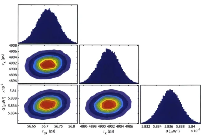
Figure 2.3. Corner plot displaying projections of the posterior probability distribution sampled by the MCMC method applied to the model in Equation 2. The diagonal panels show histograms for each of the individual parameters. The off-diagonal panels show the cross-correlations
between each pair of parameters produced by applying a kernel smoothing estimation
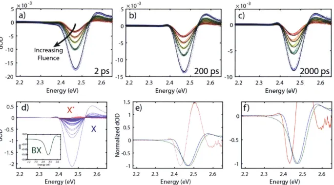
algorithm to the MCM C samples. The contour lines are 10% intervals... 43 Figure 2.4. Results of the global fit using the model in Equation 2 and the MCMC sampler. (a)-(c) Comparison of the fitted and raw data. The colored circles are raw TA spectra at a pump-probe time delay of 2, 200, and 2000 ps respectively, and the colors indicate differing pump powers from low (red) to high (blue). The black lines are the fitted spectra extracted from 100 random states of the Markov chain overlaid with some transparency. (d) Close-up view of a data point from panel a demonstrating the blurring of the fit line. The data point is not on the same scale, and its error bar is 1.17x10⁻⁵ dOD, well outside of the field of view. (e) Component spectra of the biexciton (green) and exciton (blue) states extracted from 100 random states of the Markov chain overlaid with some transparency. (f) Component spectra normalized to have the same
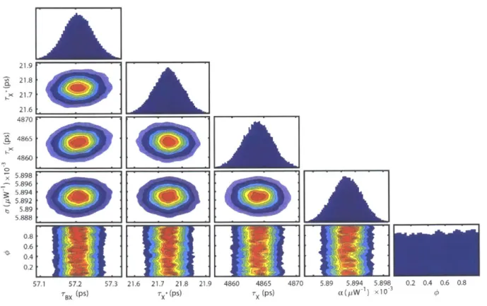
bleach am plitude for visual com parison... 45 Figure 2.5. Example of an over-specified model. Corner plot displaying projections of the
posterior probability distribution sampled by the MCMC method applied to the model 10
proposed by Equation 7. The diagonal panels show histograms for each of the individual
parameters. The off-diagonal panels show the cross-correlations between each pair of variables produced by applying a kernel smoothing estimation algorithm to the MCMC samples. The contour lines are 10% intervals. The flat posterior distribution of the parameter (p indicates an ove r-specifie d m o d el . ... 4 7 Figure 2.6. Example of an over-specified model. Results of the global fit using the model in Equation 7 and the MCMC sampler. (a)-(c) Comparison of the fitted and raw data. The colored circles are raw TA spectra at a pump-probe time delay of 2, 200, and 2000 ps respectively, and the colors indicate differing pump powers from low (red) to high (blue). The black lines are the fitted spectra extracted from 100 random states of the Markov chain overlaid with some transparency. (d) Component spectra of the two exciton states, X (blue) and X* (red), extracted from 100 random states of the Markov chain overlaid with some transparency. (inset)
Component spectra for the biexciton state. (e) Component spectra normalized to have the same bleach amplitude for visual comparison. (f) Normalized component spectra zoomed-in for better com parison of the X and BX line shapes... 48 Figure 2.7. Corner plot comparing the trion fraction parameter 0 to the minimum intensity of the X and X* component spectra. The off-diagonal panels show little random spread and a very
strong correlation between the yield parameter and both intensities as well as a strong
correlation betw een the 2 intensities. ... 49 Figure 2.8. Schematic showing the 3 components of a transient absorption signal for a
semiconductor nanocrystal prepared in the exciton (left) and biexciton (right) state... 50 Figure 2.9. Trajectories of the posterior probability for 100 walkers from (a) the tempered MCMC run used to find the global probability maximum, and (b) the non-tempered run used to sam ple the shape of the posterior probability density. ... 57
Figure 3.1. (a) Linear absorption and photoluminescence spectra for the 3 samples studies. (b) Transmission electron micrograph of a film of 10 nm NCs and (inset) high resolution TEM of a single NC. (c) Transient absorption spectra over at a series of pump-probe time delays of the 7.5
nm NCs at a pump fluence that excites an average of 1.1 excitons per NC per pulse. (d)
Transient absorption spectra at a pump fluence that excites an average of 0.2 excitons per NC p e r p u lse . ... 6 3 Figure 3.2. Transient absorption spectral dynamics of 7.5 nm NCs with a pump fluence that generates an average of 1.1 excitons per NC per pulse. The schematics illustrate the dominant
physical processes during the pump-probe delay times of the corresponding spectra. (a) Hot carrier cooling and structural relaxation, 0-2 ps. (b) Biexciton recombination (2-200 ps). (c)
Exciton recom bination (>200 ps)... 65 Figure 3.3. Comparisons of the raw data and a sample of the fits extracted from the MCMC ensemble. The colored circles are the data collected at a series of pump fluences, and the black
lines are 100 superimposed sample fits. The individual fits are indistinguishable on this scale as they all lie within the thickness of the individual lines. (a), (d), and (g) are the fits for the 10 nm
the fits for the 7.5 nm NCs at the same time delays, and (c), (f), and (i) are the same for the 6 n m N C s... 6 6 Figure 3.4. Corner plot displaying the probability distributions for each parameter and
parameter pair extracted from the MCMC analysis for the 10 nm NCs. The diagonal panels show histograms for each of the individual parameters. The off-diagonal panels show the cross-correlations between each pair of parameters produced by applying a kernel smoothing
estimation algorithm to the MCMC samples. The contour lines are 10% intervals... 68 Figure 3.5. Corner plot for the 6 nm NCs... 69 Figure 3.6. Normalized component spectra for the exciton (black trace) and biexciton (red trace) states for the (a) 10 nm, (b) 7.5 nm, and (c) 6 nm NCs. Raw component spectra for the (d) 10 nm, (e) 7.5 nm, and (f) 6 nm NCs The plots were generated by superimposing the component spectra recovered from 100 random samples of the Markov chain, and the variation among the sam ples is w ithin the w idth of the traces... 70 Figure 3.7. Size dependent properties extracted from the component spectra in Figure 3. (a) Energy difference between the biexciton and exciton component spectrum peak positions. (b) Full width a half maximum of the biexciton (red) and exciton (black) component spectra... 71 Figure 3.8. (a) Fluorescence intensity trace throughout solution-g(2
) measurement (blue). Dotted
lines denote the ranges which are independently fit to a diffusion model. Two representative fits (b-c) are shown with the corresponding biexciton to exciton quantum yield ratios. Red crosses are the average focal volume occupation parameters extracted from the diffusion fit corresponding to each sub section... 73 Figure 3.9. (a) Low-flux (0.75 pj/cm2) time-resolved emission spectrum of 7.5 nm NCs excited at 400 nm. (b) High-fux (75 pJ/cm2) time-resolved emission spectrum of 7.5 nm NCs excited at 400
nm. (c) Spectrally integrated high (purple)- and low (orange)-flux PL dynamics showing lifetime quenching at early times corresponding to multiexciton emission. The inset shows equivalent long time high- and low-flux dynamics confirming that exciton dynamics are unperturbed. (d) Comparison of spectral slices corresponding to high-flux early (0-1 ns) time (green), high-flux late (5-6 ns) time (magenta), low-flux early (0-3 ns) time (orange), and low-flux late (5-6 ns) time (cyan). The spectral positions are labeled with arrows in (a) and (b). (e) High-flux time-resolved spectrum of 7.5 nm NCs exposed to air with the inset showing early time spectra. (f) Spectral slices of an air-exposed, high-flux sample corresponding to 0-1 ns (green) and 5-6 ns (magenta). The difference between the green and magenta traces is in black. The blue dotted trace is a single Gaussian fit to the difference spectrum. A bulk CsPbBr3 perovskite emission spectrum is plotted in grey for reference... 75 Figure 3.10. Time-resolved photoluminescence traces of air-exposed samples showing the irreversibility of the red-shift. (a) Full TRPL spectrum at low flux before high flux illumination. (b) Spectrum under high-flux illumination. (c) Spectrum at low-flux after high-flux illumination. (d) PL spectrum of the 0-1 ns tim e window for (a)-(c)... 77 Figure 3.11. (a) Steady-state absorption spectra of 7.5 nm NC samples before (dotted) and after (solid) irradiation for both an air-free (blue) and air-exposed (red) sample. The inset shows the
normalized changed in the excitonic peak for the air exposed sample. (b) Representative TEM images for air-free, unirradiated (blue) and air-exposed, irradiated (red) samples. (c) Dynamic
light scattering data size distribution fits for air-free, unirradiated (blue dotted), air-free,
irradiated (blue solid), and air-exposed, irradiated (red solid) samples. ... 77 Figure 3.12. Exciton emission maxima extracted from low-flux emission spectra and aggregation emission maxima extracted from high-flux early-time spectra (demonstrated in Figure 3.9f) for three nanocrystal sizes. The inset shows the size dependent difference between the exciton and aggregate em ission features... 79
Figure 3.13. Schematic of the proposed mechanism for a repulsive interaction. As the NC size decreases, the lattice distortions associated with the individual charge carriers begins to
overlap, reducing the ability of the lattice to solvate each individual carrier... 80 Figure 4.1. (a) FSRS pulse sequence. (b) Ground-state FSRS spectrum and time-resolved FSRS gain at -6 ps and +1 ps. (c) Optical layout for the FSRS instrument. BS - beamsplitter; WP1, WP2, and WP3 - half-wave plates; PBS - polarizing beamsplitter; BBO - barium borate; YAG yttrium aluminum garnet; TEL telescope; SDC 750 nm shortpass dichroic beamsplitter; ETL -etalon; C1 and C2 - optical choppers; ND - variable ND wheel; L1-L6 - lenses (f = 1000 mm, 100
mm, 50 mm, 100 mm, 200 mm, and 50 mm respectively); POL polarizer; RR1 and RR2
-retroreflectors; OAP - off-axis parabolic mirror (f = 50.8 mm); CM1, CM2, and CM3 - concave mirror (f = 100 mm, 50 mm, and 200 mm respectively); BD - beam dump; PC - prism
compressor; ND - variable neutral density wheel; SC - sample cell... 87 Figure 4.2. (a) Schematic layout of the electronics connections. (b) Illustration of a typical data collection scheme applied to a high repetition-rate system depicting the synchronization signals and the modulation of the pump beams. The 4 interleaved spectra are labeled A-D. (c)
Illustration of the improved chopping scheme proposed in this work. Again, the 4 interleaved spectra are labeled A-D and their position at the beginning or end of the long chopping phase is d e n o te d 1-2 ... 8 9 Figure 4.3. Low-fluence FSRS data (0.95 mJ/cm2 RP, 1.75 mJ/cm 2 AP). (a) Full time-resolved FSRS
gain spectrum of fluorescein. (b) Offset FSRS gain spectra at selected time points. The ground state Raman spectrum acquired during the measurement is shown in black at the bottom of the pa nel, fo r refe re nce . ... 9 2 Figure 4.4. High-fluence FSRS data (4.0 mJ/cm2 RP, 3.5 mJ/cm2 AP). (a) Full time-resolved FSRS
gain spectrum of fluorescein. (b) Offset FSRS gain spectra at selected time points. The ground state Raman spectrum acquired during the measurement is shown in black at the bottom of the panel, fo r refe re nce . ... 9 3 Figure 4.5. (a) FSRS gain spectra at t = 6.7 ps acquired with the typical chopping scheme and the flow cell peristaltic pump turned off (orange) and on (green). The blue trace was acquired with the flow cell running and the improved chopping scheme, showing superior signal-to-noise performance. (b) Comparison of transient absorption traces collected in the chopping window A (blue) and window B (red) phases of the chopping scheme shown in Fig. 2(b) (Raman pump blocked) as described in the m ain text... 94
Figure 4.6. FSRS gain spectra at t = 6.7 ps as a function of laser repetition-rate, using 0.95
mJ/cm2
Raman pump and 1.75 mJ/cm2
actinic pump pulse fluence. (a) Data collected with constant 8 second acquisition time. (b) Data collected with the integration time scaled so that all acquisitions include the same number of pulses. The integration time was set according to the number of pulses that fall within a camera detection window, and don't scale strictly with th e re p etitio n-rate . ... 9 6 Figure 4.7. Preliminary experiments for determining the Raman pump power and time delay. (a) Ground state FSRS spectrum on the stokes side at 122 pW of applied Raman pump power over a range of stage positions. (b) Same data as (a) depicting both the stokes and anti-stokes sides. (c) Ground state FSRS spectrum at 2 different Raman pump powers at a stage position of -0.32 m m ... 9 9 Figure 4.8. Background subtraction of the time-resolved FSRS spectrum. These spectra are not normalized by the ground state FSRS spectra (i.e. they are calculated as Raman pump
on/Raman pump off with the actinic pump on). The data (green trace) and background fit from the rloess algorithm with a window size of 100 points (blue trace) are shown for an actinic pump-probe time delay of (a) 1 ps and (b) 3ps. (c) Background subtracted FSRS spectra. Peaks associated with the toluene solvent are indicated by a *, and residual Raman pump transmitted
by a side band of the etalon is indicated by **. ... 100 Figure 4.9. Time-resolved FSRS spectra of 10 nm CsPbBr3 nanocrystals, not normalized to the ground state FSRS spectrum. (a) Early-time dynamics depicting the effects of the changing resonance and polaron formation. (b) Longer time dynamics showing no change in the spectrum, and the onset of decay of the overall intensity consistent with charge carrier
reco m b in ation ... 10 2
List of Tables
Table 2.1. Kinetic parameters fit from the target analysis model with 90% credible intervals extracted from the M CM C sam pler... 43 Table 3.1. Parameters recovered from the MCMC ensembles with the 90% credible intervals
indicated, and the absorption cross-section at 400 nm calculated from the fit parameter and experim e ntal co nd itio ns. ... 67
Chapter 1 Introduction
1.1 Lead Halide Perovskites
Despite perovskite's reputation as a next-generation material, they have a long history with origins in minerology. The original perovskite material was calcium titanate, discovered in 1839 by Gustav Rose. The crystal structure was later named by another mineralogist, Lev Perovski.1 Organometal halide perovskites were developed much later in the 1990's, beginning with tin-based perovskites2 followed shortly thereafter by lead-based perovskites.3 For some time, these perovskite materials were mostly of interest for fundamental study of their electronic and magnetic properties. The use of lead halide perovskites in solar cells began in 2009, when Kojima et. al.4 first used methylammonium lead bromide and iodide perovskites as a sensitizer
in a TiO2-based solar cell. It was later discovered that lead halide perovskites are effective absorbing layers in single-junction solar cells, and the record perovskite solar cell efficiencies have risen extraordinarily quickly to 23.7% at the time of this writing.5
*Pb
Cs, MA, FA
Figure 1.1. Schematic of the lead halide perovskite unit cell.
The term "perovskite" refers to the 3-component crystal structure shown in Figure 1.1 with an ABX3 composition. The sub-lattice of the X component forms corner-sharing octahedra, with the B component in the middle of the octahedra and the A component occupying the
interstitial spaces between them. The lattice shown is a cubic perovskite lattice, where all of the angles in the octahedra are 90*, and the edge lengths are all equal. The octahedra can also be distorted, forming tetragonal or orthorhombic perovskite phases. In lead halide perovskites, the
X component forming the octahedra is a halide ion (chloride, bromide, or iodide). The B
component is generally lead for perovskites proven to be useful in device applications, but
perovskites containing other bivalent metal cations have also been synthesized. The A
component can be a cesium or an organic cation. Perovskites featuring an organic cation are
sometimes referred to as organometal halide perovskites or hybrid perovskites.
Lead halide perovskites are distinctive among bulk semiconductors in their ease of synthesis
and fabrication. Most bulk semiconductors must be grown as high-quality single crystals with
few defects. This usually requires sophisticated, energy-intensive processing involving high
vacuum or high temperatures. In contrast, a high-performing perovskite film can be fabricated
by simply spin-coating a solution of precursor components onto a substrate at room
temperature.
67Such solution processability could enable roll-to-roll or inkjet printing of small
devices. High quality single crystals of lead halide perovskites can also be grown at room
temperature via slow precipitation from a liquid solution.
The band gap of bulk lead halide perovskites varies with the halide cation. Chloride, bromide,
and iodide perovskites have band gaps in the deep blue (405 nm)
8, green (561 nm) and
near-infrared (821 nm)
9regions respectively. Alloyed perovskites can be easily synthesized by mixing
the halides used in the precursor mixtures, and they have a band gaps between the those of the
pure components.
6"
0This allows for continuous tuning of the band gap through the visible
range by synthesizing mixed Cl/Br or Br/I perovskites with different ratios of the halide
components.
1.2
Dielectric Properties and Polaron Formation
Lead halide perovskites are distinct from many other semiconductors in that the atomic lattice
is very soft, and the atomic motions are strongly anharmonic and disordered." This is most
clearly manifested in the dielectric function. Most semiconductors have a sharp resonance and
a small jump in the dielectric function in the THz region around the optical phonon frequency.
In contrast, lead halide perovskites have much broader resonances and order of magnitude
jumps in their dielectric function around the multiple phonon resonances. This feature is also
seen in ferroelectric materials. Ferroelectrics support macroscopic polarization of the atomic lattice due to correlation and ordering of microscopic dipoles."
Although perovskites may not be fully ferroelectric, these polarization effects cause the atomic lattice to respond strongly to the presence of charge carriers. The polar lattice, specifically the lead-halide octahedra, distorts around electrons and holes to "solvate" the charges in the lattice and form a polaron, a quasiparticle consisting of the charge carrier and its associated lattice distortion that moves as a unit. Polarons come in two varieties, depending on the spatial extent of the lattice deformation. Small polarons involve very strong distortions over roughly a single unit cell in the crystal. In order for the polaron to move, it must overcome a large reorganization energy, so small polarons migrate via a hopping transport mechanism. This is process is sometimes referred to as self-trapping. In contrast, large polarons involve smaller lattice distortions spanning many unit cells. Large polarons can migrate in the same way as normal charge carriers in a band-edge state, though the migration is still affected by the lattice distortion.'
Lead halide perovskites are thought to form large polarons. This results in charge carriers being protected from scattering with each other, static traps, and phonons. It is thought that this effect is partially responsible for the high performance of perovskite solar cells. The exciton binding energy is weak due to screening of the electron-hole coulomb interaction, so charge carriers can be separated easily. Screening of interactions with trap states is thought to suppress non-radiative recombination pathways, allowing for the solar cell to operate efficiently even when the perovskite material itself has a high defect density. 13-16
Although the distortion of the lead halide lattice is responsible for most of the screening in the lattice,'s there is an additional contribution when a polar organic cation, such as
methylammonium or formamidinium, is used as the A-component. The polar cation can freely rotate within its site and orient itself in response to electric fields, much like a polar liquid. Indeed, the dielectric function of methylammonium lead iodide shows another large jump in the GHz region, and the dielectric function is similar to liquid water at frequencies less than around 100 GHz.1 This reorientation is also present within the large polaron and further
-4
screens the charge carriers, although the effect is smaller than the screening due to distortion of the lead halide lattice.7
1.3 Nanostructured Perovskite Materials
Lead halide perovskites can be synthesized in a variety of nanoscale morphologies that all have distinctive properties. These take the form of OD, 1D, and 2D structures in either colloidal nanostructures or networked solids. Replacing some of the A-site cations with long chain alkylammonium salts in a slow precipitation results in the formation of a bulk quantum well-like structure consisting of 2D sheets of perovskite lattice a few unit cells thick separated by a spacer layer formed by the long-chain organic molecules.18 This can also be done in a rapid antisolvent precipitation to produce colloidal nanoplatelets lateral sizes of hundreds of
nanometers. These 2D structures exhibit strong quantum confinement with band gaps that vary dramatically with layer thickness, especially with layers between 1 and 3 unit cells thick."
Lower dimensional variants of perovskite networked solids have also been synthesized.
Adjusting the stoichiometry to ABX4 and choosing an appropriately sized organic ligand forms a networked solid of 1D perovskite nanowires separated by organic spacers. Similarly, adjusting the stoichiometry to ABX6 and choosing a suitably large organic cation forms a network of perovskite nanoclusters, where each cluster is a single unit cell. These 1D and OD structures also exhibit strong quantum confinement and have their own distinctive properties.8
a)
b)c)
-Abs
3
PIL
0CL7.5 nmr~0
< 10nm2
2.5
3
3.5
Energy (eV)
Figure 1.2. (a) Transmission electron micrograph of a film of 10 nm CsPbBr3 nanocrystals. (b) Closer view of the same nanocrystals. (c) Linear absorption and photoluminescence spectra of a size series of CsPbBr3 nanocrystals showing weak size dependence.Like many other semiconductors, colloidal perovskite nanocrystals can also be synthesized via a hot-injection method. They take the form of cubes that vary from 4-15 nm in edge length (Figure 1.2a-b).20 When made with other semiconductors, such nanocrystals are often referred to as "quantum dots." The hallmark of a quantum dot is quantum confinement that varies with the size of the nanocrystal that allows continuous tuning of the band gap over a wide range simply by changing the size of the nanocrystal. All semiconductor materials have a parameter that determines the approximate nanocrystal size where these effects become significant, known as the exciton Bohr diameter.
Lead halide perovskite nanocrystals are distinct from other semiconductor nanocrystals in that perovskites have relatively small Bohr diameters (7 nm for CsPbBr3)20, and it is difficult to synthesize colloidal nanocrystals smaller than the Bohr diameter. As a result, they are no true quantum dots, and they will not be referred to as such in this thesis. The quantum confinement effects are weak, and there is only a slight change in the absorption and emission wavelengths with nanocrystal size (Figure 1.2c).
Despite the weak confinement, perovskite nanocrystals can be made to have extremely high photoluminescence (PL) quantum yields, up to 90%. This is remarkable because perovskite nanocrystals consist of a perovskite core and ligands only. In contrast, specially engineered shells are required to produce such high PL quantum yields in other quantum dot systems. This property makes perovskite nanocrystals a material of interest for light-emitting applications, and perovskite nanocrystal LEDs have already been fabricated.
A key advantage of using a colloidal nanocrystal in a device is that numerous properties that affect device performance can be tuned by modifying the synthesis. Such properties include the size of the nanocrystal, the composition, and the surface chemistry. In this way, nanocrystals can be thought of as designer materials whose properties can be modified to suit the intended application. Unlike in a solar cell, the performance of a nanocrystal-based LED or laser depends on the nature of multiply excited states in the material, because such applications involve high carrier injection rates. Knowledge of how the synthetic handles affect the energetics and
dynamics of these excited states would enhance our ability to design a perovskite nanomaterial best suited for light emitting applications.
The subject of this work will be CsPbBr3 perovskite nanocrystals. Like other colloidal
semiconductor nanocrystals, CsPbBr3 nanocrystals are synthesized via a hot-injection synthesis. A solution of precursors and the desired surface ligand is heated to a controlled temperature, and a concentrated solution of the remaining precursor is rapidly injected into the mixture. The size of the nanocrystals is generally controlled by adjusting the precursor stoichiometry,
reaction temperature, or reaction time. In the case of CsPbBr3, the growth is quite fast, and the size is best controlled using the reaction temperature.20 The key recent innovation in CsPbBr
3 synthesis is the use of the surface chemistry to improve stability. Most semiconductor
nanocrystals are capped with a labile surface ligand with a long alkyl chain and charged capping group. For CsPbBr3, this would be an alkylammonium ligand. The stability was improved by using a strongly bound zwitterionic ligand.2'
1.4 Electronic Structure of Semiconductor Nanocrystals
When calculating the electronic structure of a bulk semiconductor to get the shapes of the valence and conduction bands, the crystal is assumed to be infinite and a periodic boundary
condition is employed. Although the CsPbBr3 nanocrystals are not strongly quantum confined in the same way as traditional quantum dots, they are small enough that they should not be assumed to be infinite. As such, we use the same picture as for other quantum dots for
modeling the electronic structure, as developed by Hu et. al.2 2
We begin by evaluating the single-body electron and hole states which describe the manifold of filled and empty states in the ground state. They also effectively describe the energy of a lone electron or hole on a charged nanocrystal. As in any quantum mechanical system, these are
described by the time-independent Schrodinger equation. 'H = ET
E is the energy of each state represented by the wavefunction, 4W. The Hamiltonian, R, which
describes the system can be broken up into kinetic energy, electron-lattice interaction potential, and confinement potential portions. The effects of the electron-lattice interaction potential, Viattice, can be well approximated by offsetting the energies calculated from the other components by the bulk band edge positions. This just leaves the kinetic energy (RKE) and
confinement potential (Vconfinement) portions. As a first approximation, we can assume an infinite well potential that is 0 inside the nanocrystal and oo outside of it. In this case, the confinement potential and kinetic energy terms together form the classic particle-in-a-box problem. Since perovskite nanocrystals are cubes, we use the solution for a cubic box. The confinement energies are simply the sum of the energies for a one-dimensional particle in a box for each of the three dimensions. By convention, we set the bulk valence band maximum to be the point of zero energy, which offsets the energies of the electron states by the bulk band gap, Eg. Thus the single-body electron and hole energies are as follows.
E,= h 2
(n
+n2+ )n + E+me 2(0.2)
h2
The energies are a function of the nanocrystal edge length, L, the plank constant, h, and the effective mass of each carrier, m*. The "e"and "h" subscripts indicate the electron and hole energies respectively. Finally, each state is defined by three independent quantum numbers, nx, ny, and n, which can values of positive integers (1,2,3...). In the case of CsPbBr3, the electron and hole have near-identical effective masses, so the electron and hole energy states are very similar other than the band gap offset.
When a nanocrystal absorbs a photon, an electron in the conduction band and a hole in the valence band are created simultaneously. Taken together, they are often referred to as an exciton. Since both the electron and hole are present in the exciton state, we can construct pair states that describe the exciton as a hole. We refer to these as confinement states to indicate
that they contain only the confinement potential. The total energy, Ex, is then the sum of the electron and hole energies.
Ex = E +Eh (0.3)
However, in addition to the terms described in the Hamiltonian above, we must now add the electron-hole coulomb interaction to obtain the correct energies. This problem is impossible to solve analytically but can be solved approximately. This is done by using the confinement states described above as a basis set and calculating the interaction potential matrix element for each combination of electron and hole states. This gives an exciton Hamiltonian matrix, Nx.
(Ti V_, IT) (T, V,-h I 2) --- (T e-h nT,)1
-= 2 V- I,) (T 2 V -hI 2) .. (T2 V-_ IT,) (0.4)
Lj are pair wavefunctions that represent the electron and hole in states defined by the 6 quantum numbers in equation 1.2. Ve-h is the electron-hole coulomb potential. Once the matrix
has been calculated, the state energies including the coulomb interaction can be calculated by diagonalizing the Hamiltonian matrix. The reason this is an approximation is because we have had to truncate the calculation at a finite number of the confinement states.
The difference in energy between the lowest-lying exciton state with and without the electron-hole coulomb interaction can be thought of as the exciton binding energy. This represents the energy difference between having a bound exciton on one nanocrystal and an unbound electron and hole on two separate nanocrystals. Note that this is different than the exciton binding energy in a bulk semiconductor, which is the energy difference between a bound exciton and a free electron and hole in delocalized continuum states. There are no true continuum states in a nanocrystal as it is too small for the electron and hole to separate far enough to not be influenced by coulomb attraction, so a "free carrier" state does not exist on a single isolated nanocrystal in solution.
These single exciton states can be used to describe optical absorption and emission under the weak optical excitation conditions that are relevant for solar cell applications or in most photoluminescence experiments. However, under stronger optical or electronic excitation, as might be encountered in a laser or LED, higher excited states can be created where multiple excitons reside on a single nanocrystal. For the purposes of this work, we focus on the biexciton states, where two excitons are generated on the nanocrystal.
1.5 Biexcitons and Optical Gain in Nanocrystals
The energies of the biexciton states can be modeled in the same fashion as the exciton states in the previous section. This time, each biexciton states contains two electrons and holes, and the coulomb potential for all 4 carriers is used to calculate the matrix element. This includes
electron-electron repulsion, hole-hole repulsion, and electron-hole attraction interactions. Once again, matrix diagonalization gives the energies of the states. As with the exciton, we can define a biexciton binding energy as the energy difference between the lowest-lying biexciton state and twice lowest-lying exciton state. This represents the energy difference between a
bound biexciton and two excitons on separate nanocrystals.22-2 4
Since the biexciton binding energy represents the coulomb interaction between two neutral excitons, it is generally small and can be either sign (i.e. it can be either attractive or repulsive). The sign of the interaction depends on the interplay between the coulomb interactions among all 4 carriers and other higher-order effects. As an example, theoretical calculations based on small CdSe quantum dots found that the biexciton binding energy is always positive (attractive) in that system and increases with decreasing quantum dot size.22,23
Optical gain in semiconductor nanostructures is understood to be highly dependent on the properties of multi-excitonic states. For example, optical gain in CdSe quantum dots has been characterized extensively. Measurements of the optical gain threshold in this system revealed that quantum dots begin to lase when an average of more than 1 exciton is injected into each dot. Therefore, optical gain results from a transition between the biexciton and exciton states.2 4
,25 CdSe quantum dots have a bound biexciton state with a binding energy of 5-30 meV2 3
exciton-to-biexciton optical transitions that aids in the buildup of optical gain as the emission competes less strongly with absorption. Due to this effect, a more strongly bound biexciton should lead to a lower optical gain threshold. Here, CsPbX3 NCs show great promise, as biexciton binding energies of 30-100 meV have been reported.28- 0 However, the proposed presence of a strongly bound biexciton conflicts with other known characteristics of these materials. For one, the exciton binding energy metal halide perovskites is quite low, <12 meV in the bulk material and around 20 meV in NCs, due to strong dielectric screening in these materials.3 1
-3 3 More broadly,
the dielectric properties of the lattice as well as polaron formation are thought to suppress coulombic interactions between carriers, defects, and phonons.1 1,1s,3 4
An exceptionally strong biexciton binding energy is thus surprising since coulomb interactions are intrinsically weak due to screening by the perovskite crystal lattice. Furthermore, most perovskite NCs are only weakly quantum confined leading to very little enhancement of exciton and biexciton binding energies. Similarly, phenomenological studies of several properties including hot carrier relaxation, electron-phonon coupling, and optical gain show that the carrier dynamics in perovskite NCs are often well represented by bulk-like continuum models rather discrete excitons and multiexcitons.33 3s,36 The case of optical gain stands out in
particular where Geiregat et. a/. states that the gain threshold expressed as a carrier density is independent of NC size over a wide range.3s In contrast, strongly bound excitons and
multiexcitons would imply a gain threshold that is constant in the number of excitations per NC, resulting in a gain threshold that varies with NC size.
1.6 Experimental Characterization of Biexciton States in Nanocrystals
Femtosecond transient absorption spectroscopy (TA) has proven to be an effective technique for observing excited states in semiconductor materials. It has sufficient time resolution to capture the sub-ns dynamics that such multiply excited states often have and the sensitivity of the spectra to electronic dynamics yields significant useful information. Like most ultrafast spectroscopy techniques, TA is a pump-probe experiment involving two laser pulses separated by a controllable time delay. The first pulse, the pump, excites the sample and creates the excited states of interest. The second pulse, the probe, interrogates the state of the sample
after a known time delay. For TA, the pump pulse is set to be at or above the band gap of the sample to generate excitons. The probe is a broadband supercontinuum pulse that measures the optical absorption of the sample over a range of wavelengths. By modulating the pump and comparing the transmitted probe light with and without the pump pulse, we can measure a differential absorption spectrum (Figure 1.3).
-o0
-2--3x1
-2.2 2.3 2.4 2.5 2.6
Energy (eV)
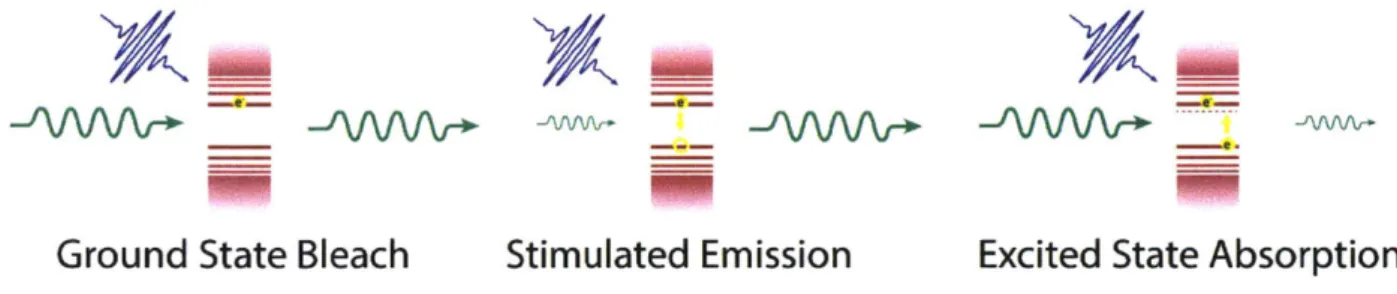
Figure 1.3. Schematic of a transient absorption experiment and a typical differential spectrum. Figure 1.4 shows an illustration of the 3 components that contribute to a TA signal. The first, ground state bleach, arises because once an exciton has been excited by the pump, the same exciton cannot be excited again. This leads to a bleach or loss of absorption that appears as a negative signal in the TA spectrum. The second is a stimulated emission signal, where the excited exciton can recombine and emit into the probe beam. This will also appear as a
negative feature in the TA spectrum. The third is excited state absorption (ESA), where a second photon is absorbed to create a higher excited state. In the measurements in this work, ESA creates a new exciton which will have a different absorption spectrum than the first exciton. This will appear as a positive feature in the TA spectrum.
-/&rnJ-
_rGround State Bleach
Stimulated Emission
Excited State Absorption
Figure 1.4. Schematic of the three contributions to a transient absorption spectrum.
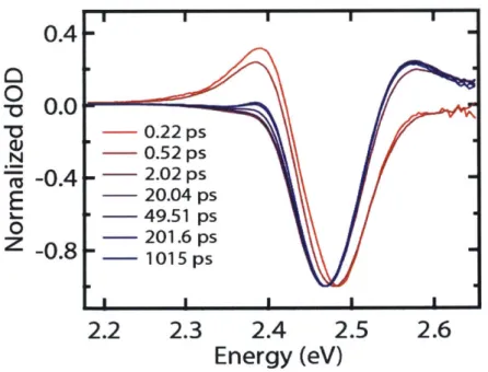
The depiction of ESA in Figure 1.4 shows how the TA spectrum can contain information about the biexciton state, as ESA in a nanocrystal with one exciton probes the exciton-to-biexciton transition involved in optical gain. The typical strategy for extracting this information involves a first-principles-driven approach, where a model for the states and their dynamics is first assumed to fit parameters to the data. A series of TA spectra of CsPbBr3 nanocrystals at several pump-probe delay times is shown in Figure 1.5. The feature of note here is the induced
absorption on the red side of the main peak that appears immediately after photoexcitation and decays in 1-2 ps. This feature is universally seen semiconductor systems when excited well above the band gap. The following physical picture is thus invoked: Immediately after
photoexcitation, the spectral shift due to the biexciton binding energy becomes visible in the red-side induced absorption. Its visibility is aided because the bleach signal due to filling of the band-edge exciton does not occur until the exciton created by the pump relaxes to the band edge, a process that generally takes 1-2 ps.
I
0.4
0
-
0.
0-0
0.22 ps
N- 0.52 ps -0.4 . -2.02ps
E
--
20.04 ps
-
49.51 ps
0
-
201.6 ps
-0.8 --
1015 ps
2.2
2.3
2.4
2.5
2.6
Energy (eV)
Figure 1.5. Transient absorption spectra of 7.5 nm CsPbBr
3nanocrystals normalized to the same bleach
intensity.
The overall shape
2 7or dynamics
3 7of this induced absorption feature are fit to extract
information about this biexciton-induced shift. Although this is not the true biexciton binding
energy, its dependence on material parameters is thought to correlate with the behavior of the
true biexciton binding energy. A shape for the absorption spectrum of the exciton-biexciton
transition must be assumed to execute the fit. In the case of CdSe, the spectrum was assumed
to be identical to the measured linear absorption spectrum shifted in energy by a biexciton
shift. Sewall et. al. estimated biexciton binding energies of 10-30 meV in CdSe quantum dots,
and combined measurements on a size-series of quantum dots with a theoretical
understanding exciton state manifold's fine structure to draw several in-depth conclusions
exciton and biexciton dynamics in these materials.
37More recently, a similar strategy has been applied to cesium lead halide nanocrystals. In this
case, the shape of the of both the linear absorption and the biexciton absorption spectra are
assumed to be gaussians with the same width, shifted by a biexciton binding energy.
28,2 9,38
A
biexciton binding energy is then extracted by either directly fitting the two gaussians to a TA
spectrum immediately after photoexcitation or by extracting the information just from the
relative magnitudes of the bleach and ESA features. Such strategies led to the conclusion that
I I
biexcitons in perovskite nanocrystals have a binding energy of 40-100 meV, which would make them exceptionally strongly bound. As noted in section 1.6, these strong binding energies are inconsistent with empirical observations of free-carrier-like behavior in these nanocrystals. Thus, this physical understanding of TA data and the information it contains about biexciton states is too simplistic to accurately capture the physics of the systems.
The assumption that the exciton and biexciton absorption spectra are identical in shape or line width is particularly problematic because it makes many assumptions about the underlying of the physics of the material. The shape of the absorption spectrum is determined by adding up the many possible transitions between each manifold of states. The width of each transition has contributions from homogeneous and inhomogeneous broadening. Homogeneous broadening arises due to quantum mechanical coupling of the state of interest to other electronic states as well as vibrational states (phonons) in the material. Inhomogenous broadening arises from differences in the average position of each energy level between nanocrystals in the ensemble. Size dispersity is usually the main contributor. Postulating that the exciton and biexciton absorption spectra are identical, shifted versions of each other presupposes that these effects have identical influences on the optical properties of the exciton and biexciton states and that each state has an identical manifold.
Another problem is that the TA data at sub-ps pump-probe time delays will not reflect the energetics of a biexciton state when it emits in an LED or a laser. The emission process is much slower, generally on a hundreds of ps time scale. Furthermore, there are ultrafast processes that are actively occurring within the first ps that are not relevant to biexciton emission, including the decay of electronic coherences excited by the pump pulse and hot carrier relaxation.36 The perovskite materials also undergo considerable structural relaxation on this time scale, and it generally takes 1-2 ps for the polarons to fully form. Extracting information about the biexciton states from TA spectra at longer time delays would yield a more accurate characterization of the emission from those states.
These complexities inherent in the excited state dynamics and energetics of perovskite nanocrystals make it impractical to use a first-principles-driven approach to interpreting TA
data. There are too many factors to consider and it is not clear how each will affect the
measured spectra. Furthermore, extracting a single parameter in the biexciton binding energy or spectral shift does not provide sufficient information to understand how the TA spectra are consistent with other empirical observations of the material properties. Instead, we require a data driven approach where we extract the full spectrum of the biexciton state without making any postulate as to its shape. Such an approach should require as few assumptions as possible and provide a framework to vet and verify these assumptions. The richer information content of the full biexciton spectrum allows for a more thorough analysis of the energetics of the biexciton state and how it relates to other known fundamental physics in these materials.
1.7 Thesis Overview
In this thesis, we develop and demonstrate a data-driven approach to characterizing the energetics and dynamics of biexciton states in CsPbBr3 nanocrystals using TA spectroscopy. We then use the understanding developed using the TA data to guide experiments using other techniques and further examine the physical phenomena that influence these excited states. In Chapter 2, we describe our data-driven method in detail and demonstrate its effectiveness in extracting spectral information about CsPbBr3 nanocrystals. The method combines the target analysis fit commonly employed in organic systems with Bayesian inference and a Markov chain
Monte Carlo sampler to accurately characterize the model uncertainty and vet the model itself. In Chapter 3, we apply the analysis developed in Chapter 2 to a size-series of CsPbBr3
nanocrystals to extract the biexciton and exciton component TA spectra as a function of nanocrystal size. We find that the exciton and biexciton spectra have distinctive shapes, in contrast with the common assumption about these spectra. The biexciton spectra a broader and slightly blue-shifted from the exciton spectrum, and the broadening and blue-shifting both increase as the nanocrystal size decreases. This suggests that the exciton-exciton interaction is repulsive rather than binding, but red-shifted optical gain can still be observed from the broader red tail of the biexciton emission spectrum. We verify this with our own time-resolved photoluminescence experiments. In contrast to other reports, we do not see a dramatically red-shifted emission feature when exposure to the sample to the environment is well controlled, and we conclude that previously observed red-shifted emission features arose from sintering of
the nanocrystals into bulk-like microcrystallites. In Chapter 4, we propose and discuss in detail
the development of an experiment to verify our hypothesis for why the exciton-exciton
interaction is repulsive - the effect of polaron formation. We describe the development of a
femtosecond stimulated Raman spectroscopy experiment to directly observe polaron formation
and the challenges of performing this technique at high repetition rate. We conclude with a
brief discussion of the stimulated Raman spectra of CsPbBr
3nanocrystals, which require further
experiments to yield the desired information. The central goal of this thesis is to describe a
more careful approach to analyzing spectroscopic data. In short, using first-principles to
generate a series of assumptions about a complex system can lead to incorrect interpretation
of the data. Instead, the data should be first be parsed to separate the information relevant to
the experiment using as few assumptions as possible. Once this is done, the data can guide the
use of first-principles in the interpretations.
Chapter 2 Modeling Transient Absorption Data by Markov Chain Monte
Carlo Sampling and Target Analysis
The basis of this chapter has been published as:
M.N. Ashner, S.W. Winslow, J.W. Swan, and W.A. Tisdale, "Markov Chain Monte Carlo Sampling for Target Analysis of Transient Absorption Spectra." J. Phys. Chem. A
2.1 Introduction
Transient absorption (TA) spectroscopy is a broadly used technique for characterizing excited-state dynamics in a large variety of chemical systems. A small sampling of applications include understanding charge carrier transport in photosynthetic complexes,39,40 exciton multiplication processes in small organic molecules,4 1
,4 2 and optical gain in semiconductor
nanomaterials. 2
,2 8,35 Analyzing TA data often involves performing some kind of fitting routine that can vary in complexity depending on the characteristics of the spectra and information desired. In the simplest case, with a single or few well-separated spectral features, the data at selected wavelength points can be fit to one or more exponential decay models. However, TA spectra tend to be broad and have complex line shapes, so the spectra of different components often partially overlap. A common technique to disentangle the overlapping TA spectrum and simultaneously recover the spectra and dynamics of each component is to perform global or target analysis.43 Because the component spectra often have some distinguishing features in organic systems, the model results can be qualitatively verified against the raw data.
Inorganic and solid state systems provide a challenge because their excited state characteristics are often encoded in subtle changes of the spectral line shape and complex dynamics. For example, the system considered in this work is the energetics and dynamics of biexciton states in CsPbBr3 perovskite nanocrystals. 20,21 Several studies have used TA spectroscopy to attempt to measure the biexciton lifetimes and binding energies in these materials. 28
-30
,38 The data
analysis generally involves invoking a physical argument to propose a feature assignment to obtain the binding energies and fitting the intensity of the single bleach feature to some number of exponential decays to obtain the biexciton lifetimes. In contrast, a global or target analysis technique like that used for organic systems would allow interpretation of the data without having to propose a feature assignment a priori. However, given that the spectral
features are nearly entirely overlapping with few to no independent parts, qualitative
evaluation of the fit quality is much more difficult, complicating model selection and making it more difficult to evaluate if data have been overfit. Overcoming this challenge requires a method to characterize the uncertainty of the fit in a way that is straightforward to interpret. There are two common methods for performing a global fit, each with their own procedures for characterizing uncertainty. The first uses a linear least-squares algorithm to find the component spectra nested within a nonlinear least-squares optimization to fit a proposed kinetic model.4 3 Although many nonlinear optimizers will assign goodness-of-fit metrics, these are calculated from the Hessian of the objective function (matrix of second-order partial derivatives), or effectively its curvature. Due to the nested linear least-squares problem, the Hessian cannot be analytically evaluated. Numerical estimations of the Hessian depend on the step size at
convergence, and may not accurately capture the uncertainty in the fit parameters if the
objective function is non-monotonic on the relevant scale. Furthermore, the solution yielded by a nonlinear optimizer can vary with the initial guess, especially if multiple disparate solutions give similar amounts of error.
The second method employs a singular value decomposition (SVD) of the data yielding a set of component spectra and amplitudes that can be fit to a kinetic model if desired.4 4 46 SVD is powerful because it requires no assumption of a physical model, and the number of significant components can be determined from the decomposition. It is also robust to noise in the data, and there are statistical methods for characterizing uncertainties in the spectra and amplitude vectors produced in the decomposition.4 '47 However, SVD is a purely mathematical
construction that is not bound by physical constraints. Consequently, SVD can sometimes yield non-physical results. For example, applying SVD to the data in this work produced amplitude profiles for major components that changed sign and did not decay to zero amplitude at long times. Furthermore, a multiple parameter fit to the amplitude vectors suffers from many of the same problems noted above, such as the lack of a reliable way to determine the uncertainty in extracted fit parameters.