Combined Impact of Heterogeneous Lifetime
and Gettering on Solar Cell Performance
The MIT Faculty has made this article openly available.
Please share
how this access benefits you. Your story matters.
Citation
Morishige, Ashley E. et al. “Combined Impact of Heterogeneous
Lifetime and Gettering on Solar Cell Performance.” Energy Procedia
77 (2015): 119–128.
As Published
http://dx.doi.org/10.1016/j.egypro.2015.07.019
Publisher
Elsevier
Version
Final published version
Citable link
http://hdl.handle.net/1721.1/107393
Terms of Use
Creative Commons Attribution-NonCommercial-NoDerivs License
1876-6102 © 2015 The Authors. Published by Elsevier Ltd. This is an open access article under the CC BY-NC-ND license (http://creativecommons.org/licenses/by-nc-nd/4.0/).
Peer review by the scientific conference committee of SiliconPV 2015 under responsibility of PSE AG doi: 10.1016/j.egypro.2015.07.019
Energy Procedia 77 ( 2015 ) 119 – 128
ScienceDirect
5th International Conference on Silicon Photovoltaics, SiliconPV 2015
Combined impact of heterogeneous lifetime and gettering on solar
cell performance
Ashley E. Morishige
a, Hannes Wagner
a, Jasmin Hofstetter
a, Ibrahim Avci
b,
Carlos del Cañizo
c, Tonio Buonassisi
a,*
aMassachusetts Institute of Technology, 77 Massachusetts Ave., Cambridge, MA 02139, USA bSynopsys, Inc., 690 East Middlefield Road, Mountain View, CA 94043, USA cInstituto de Energía Solar, Universidad Politécnica de Madrid, 28040 Madrid, Spain
Abstract
We couple numerical process and device simulations to provide a framework for understanding the combined effects of as-grown wafer impurity distribution, processing parameters, and solar cell architecture. For this study, we added the Impurity-to-Efficiency simulator to Synopsys’ Sentaurus Process software using the Alagator Scripting Language. Our results quantify how advanced processing can eliminate differences in efficiency due to different as-grown impurity concentrations and due to different area fractions of defective wafer regions. We identify combinations of as-grown impurity distributions and process parameters that produce solar cells limited by point defects and those that are limited by precipitated impurities. Gettering targeted at either point defect or precipitate reduction can then be designed and applied to increase cell efficiency. We also visualize the post-processing iron and total recombination distributions in 2D maps of the wafer cross-section. PV researchers and companies can input their initial iron distributions and processing parameters into our software and couple the resulting process simulation results with a solar cell device design of interest to conduct their own analyses. The Alagator scripts we developed are freely available online at http://pv.mit.edu/impurity-to-efficiency-i2e-simulator-for-sentaurus-tcad/.
© 2015 The Authors. Published by Elsevier Ltd.
Peer review by the scientific conference committee of SiliconPV 2015 under responsibility of PSE AG.
Keywords: efficiency; iron; lifetime; phosphorus diffusion gettering; photovoltaics; processing; Sentaurus TCAD; silicon; simulator; solar
* Corresponding author. Tel.: +1-617-324-5130
E-mail addresses: [email protected]; [email protected]
Available online at www.sciencedirect.com
© 2015 The Authors. Published by Elsevier Ltd. This is an open access article under the CC BY-NC-ND license (http://creativecommons.org/licenses/by-nc-nd/4.0/).
1. Introduction
Multicrystalline silicon (mc-Si) wafer quality varies widely. Total impurity concentrations and the area fraction of high defect density [1-3] both impact solar cell performance. Poorly performing areas are disproportionately detrimental [4], and wafers with higher defect concentrations are not sufficiently remediated by standard gettering [5]. Thus, treating all mc-Si wafers with the same process results in lower average efficiencies with a wider standard deviation [6]. Sorting wafers by quality, defined by the area fraction of high dislocation density, with inline photoluminescence imaging can enable better statistical process control and smaller standard deviations in cell performance [1-3]. A fast, 1D gettering model, the Impurity-to-Efficiency (I2E) Simulator [7] is a powerful tool for process optimization [8,9], but it does not capture 2D effects. Additionally, 2D simulations enable analysis of gettering in advanced cell architectures including Passivated Emitter and Rear Cell (PERC) and Interdigitated Back Contact. For this study, we developed a 2D version of the I2E Simulator for use with Synopsys, Inc.’s Sentaurus TCAD simulation software. We couple 2D phosphorus diffusion gettering (PDG) and solar cell device simulations to define effective gettering of mc-Si wafers for two different wafer sets. Wafers in Scenario A have different total iron concentrations [Fe0] but the same area fraction of dislocation-rich grains (e.g. from different ingot heights but
similar crystal structure). Wafers in Scenario B have different area fractions of dislocation-rich grains but the same [Fe0] (e.g. same ingot height but from different bricks). Our results present a pathway for manufacturers to identify
optimal processing for wafers sorted by total impurity content and by the area fraction of defective regions.
2. Simulation models
To simulate in 2D the redistribution of iron impurities during solar cell processing, we added the kinetics and thermodynamics of precipitates, interstitials, and their redistribution during phosphorus diffusion gettering as defined in the Impurity-to-Efficiency Simulator [7,10] to Synopsys’ Sentaurus Process via the Alagator Scripting Language [11]. The process simulation results are passed to Sentaurus Device [12] to simulate the performance of a PERC solar cell architecture. The wafer is p-type, with a resistivity of 2 :-cm and a thickness of 180 μm. A distance of 1.2 mm is assumed between two front grid finger contacts, while local rear contacts are 600 μm apart. Further details of the device architecture and simulation input parameters can be found in [13,14]. We explicitly calculate recombination due to interstitial iron (Fei) and the carrier lifetimes associated with iron-silicide precipitates (Fep),
and we assume a uniform 2 ms background lifetime to account for other homogeneously distributed recombination sources. The rest of the model parameters are taken from well-known physical models or fitting to experimental values.
3. Simulation scenarios
We simulated three PDG time-temperature (t-T) profiles, each tailored to optimize iron removal for different [Fe0]. All three profiles consisted of a 30-minute isothermal phosphorus diffusion step at 840°C followed by a linear
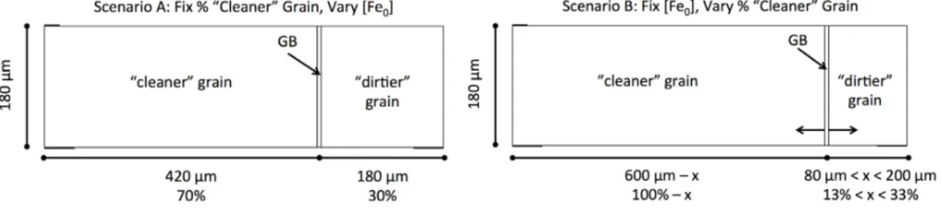
cool to 500°C. The cooling rate was varied such that the cool took 5, 20, or 100 minutes, with longer cooling times tailored to higher impurity contents. To analyse the effect of different post-processing iron distributions on efficiency, we simulated two different material Scenarios. In both Scenarios, we simulate a 600 μm-wide simulation domain with three wafer regions: (1) a lower impurity content “cleaner” grain, consistent with low dislocation density; (2) a 6 μm-wide grain boundary (GB); and (3) a higher impurity content “dirtier” grain, consistent with high dislocation density. We assumed spherical iron-silicide precipitates with an initial radius of 30 nm [8]. From the initial precipitate radius and the initial [Fep] in each wafer region, we calculated a spatial precipitate density, which
remains constant as the simulated process proceeds. The precipitate densities vary several orders of magnitude across the three wafer regions.
In Scenario A (Fig. 1 (left)), the fraction of the wafer that was “cleaner” (low dislocation density) was fixed at 70%, and the as-grown total wafer-level iron concentration, [Fe0], was varied between 4×1012 cm-3 (middle of a
mc-Si ingot) and 1×1015 cm-3 (top of a mc-Si ingot). [Fe
0] as a function ingot height was calculated as in [8], and these
Fe concentrations are typical for a cast mc-Si ingot [8]. The average [Fei] for the chosen impurity levels varies
between 5×1010 cm-3 and 7.5×1012 cm-3 [8], so we defined the “cleaner” grain as having [Fe
Ashley E. Morishige et al. / Energy Procedia 77 ( 2015 ) 119 – 128 121
average while the “dirtier” grain has twice as much [Fei] as the average. The “cleaner” grain was defined as having
[Fep] = [Fei]/10. The “dirtier” grain (high dislocation density) had [Fep] = [Fei]×50. The “cleaner” grain [Fep] thus
varies between 5×109 cm-3 and 7.5×1011 cm-3, and the dirtier grain [Fe
p] ranged from 1×1013 cm-3 to 1.5×1015 cm-3,
consistent with experimentally observed impurity variations within an ingot [15]. The GB was modelled with a low [Fei] = 1010 cm-3 because the high spatial density of precipitates facilitates precipitation. Finally, the [Fep] in the
grain boundary was calculated to achieve the target wafer-level [Fe0]. The GB [Fep] varied from 9.5×1013 cm-3 to
5.4×1016 cm-3, consistent with experimental and simulated values [16].
Fig. 1. Simulated PERC wafer structure cross-section views for Scenarios A (left) and B (right). The thick, short black horizontal lines at the upper left and bottom corners of the structure are metal contacts.
In Scenario B (Fig. 1 (right)), the as-grown wafer-level [Fe0] was fixed, and the area fraction of the cleaner grain
was varied between 67% and 87%. Two cases with different total [Fe0] were simulated: 1) 2×1013 cm-3 representing
wafers in the middle of a typical mc-Si ingot, and 2) 1.65×1014 cm-3 representing wafers from near the top of the
ingot [8]. The [Fei] in each part of the wafer was selected as in Scenario A. The [Fep] values for the [Fe0] = 2×10¹³
cm-3 and 1.65×1014 cm-3 from Scenario A were used in the 70% “cleaner” grain simulations in Scenario B. Then, as
the area fraction of the “cleaner” grain was increased, the [Fep] in the “cleaner” grain was decreased while that in the
“dirtier” grain was increased to maintain a constant wafer-level average [Fe0]. Precipitated iron in the “cleaner” grain
thus ranged from 4×1011 cm-3 down to 1×1010 cm-3 while that in the “dirtier” grain ranged from 3.5×10¹⁴ up to
9.3×1014 cm-3.
4. Simulated solar cell efficiencies
The solar cell efficiencies for each of the above-described scenarios were simulated. For both scenarios, the combination of initial iron distribution and gettering time-temperature (t-T) profile influences device efficiency.
For Scenario A (Fig. 2), as the total as-grown [Fe0] increases, the efficiency decreases. The 5 min cool results in a
wide efficiency range of 3.5% absolute. A process that is just 15 min longer results in significant increase in efficiency and decrease in variation. For a 5 min cool, only wafers from near the middle of the ingot reach an efficiency 20%, while for a 20 min cool, all wafers up to 85% ingot height reach an efficiency 20%, increasing the yield of high-performance wafers. For example, for a specific ingot height of 90% (as-grown [Fe0] = 1014 cm-3), the
20 min cool achieves a 2% absolute gain in efficiency compared to the 5 min cool. The 100 min cool achieves another 1% absolute, but at the expense of a significantly longer process. These results are consistent with those in [8], with the results updated to explicitly include the effect of recombination due to iron-silicide precipitates, an effect that is especially important for high [Fe0] found at high ingot heights.
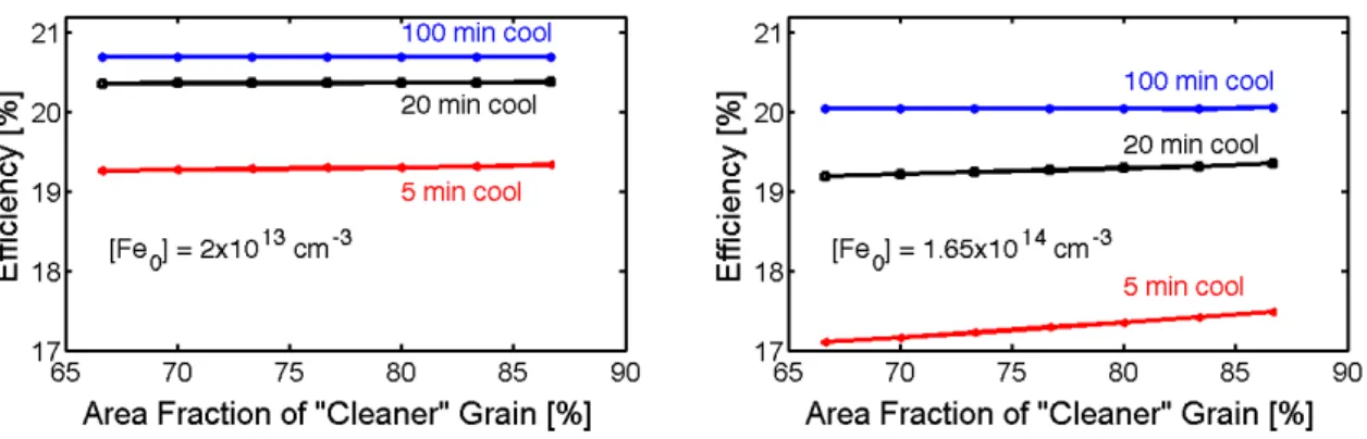
For Scenario B (Fig. 3), for a given cooling time, as the area fraction of “cleaner” grain area increases, efficiency is unchanged except for the 5 min cool for the higher [Fe0] = 1.65×1014 cm-3. For the lower [Fe0] = 2×1013 cm-3, as
cooling time increases, the efficiency increases, but the area fraction of “cleaner” grain appears to have no effect. For the higher [Fe0] = 1.65×1014 cm-3, as the area fraction of “cleaner” grain increases, the efficiency increases by 0.4%
absolute for the 5 min cool and 0.16% absolute for the 20 min cool. The slow 100 min cool shows no visible difference as the area fraction of “cleaner” grain increases.
Fig. 2. Scenario A – Cell efficiency vs. % ingot height and as-grown total [Fe0] for different PDG t-T profiles. As the [Fe0] increases, cell
efficiency decreases significantly. As the cooling time from 840°C to 500°C increases, the cell efficiency noticeably increases.
Fig. 3. Scenario B – Cell efficiency vs. area fraction of “cleaner” grain for different PDG t-T profiles. For lower [Fe0] = 2×1013 cm-3, efficiency
does not change with area fraction of “cleaner” grain, but a longer cooling time does increase efficiency. For the higher [Fe0] = 1.65×1014 cm-3, a
larger area of “cleaner” grain is predicted to increase efficiency, but the length of the cool down has a much larger effect.
5. Discussion
Solar cell efficiency depends on both the initial Fe distribution and the applied gettering process. For all the scenarios considered here, two important trends hold: 1) The “dirtier” grain (on the right) is highly recombination active and 2) as the cooling time increases, the fraction of the cell that is significantly recombination active decreases. These trends are illustrated by a representative example in Fig. 4.
Fig. 4. Total Recombination Rate across the wafer cross-section – Scenario A, 75% ingot height after each gettering process. For the 5 min cool, much of the bulk is highly recombination active. For the 100 min cool, the back contacts (lower corners) and the “dirtier” grain (right side of
Ashley E. Morishige et al. / Energy Procedia 77 ( 2015 ) 119 – 128 123
We observe that there are two main lifetime-limiting components after processing: one related to point defects and one related to precipitates. Once we identify which of these dominate after a given process, we can design gettering that is targeted at either point defect or precipitate reduction to increase solar cell efficiency [9]. Recombination at precipitates increases with precipitate size and spatial density [7]. The precipitate spatial density is high in the “dirtier” grain and the area fraction of the “dirtier” grain is at least an order of magnitude greater than that of the GB, so the precipitate-limited lifetime in the “dirtier” grain can limit efficiency. Fe point defects are highly recombination active in p-type Si [17], and they are more continuously distributed throughout the bulk of the wafer. To understand the overall lifetime trends, we consider an average bulk [Fei] to represent this distribution. Our
simulations model Fei atoms as single defect with an energy level at 0.38 eV with capture cross sections of 1.3×10⁻¹⁴
cm2 (electrons) and 7×10-17 cm2 (holes) [18,19]. In Sentaurus Device, the trap models explicitly account for the
occupation and the space charge stored on traps while SRH lifetime models neglect these effects [12]. Nonetheless, we compare the electron lifetime due to precipitates in the “dirtier” grain and Shockley-Read-Hall (SRH) recombination due to the average [Fei] in the bulk. The precipitate lifetime model is from [7], and we assume a
homogenous injection level of 4×1013 cm-3 in the device at maximum power point and capture cross-sections of Fe i
as stated above for the SRH lifetime. Differences in the trap recombination and SRH lifetime models may account for any discrepancies between the efficiency trends in Fig. 2 and 3 and the lifetime trends in Fig. 5 and 6.
For a given combination of initial Fe distribution and gettering process, the defect lifetime that is lower (point defects or precipitates) limits the effective lifetime. The point defect-related and precipitate-related minority carrier lifetimes and the total effective lifetime given by the inverse of the harmonic sum of the precipitate, point defect, and background lifetimes are shown in Figs. 5 and 6.
For Scenario A (Fig. 5), Fei limits the lifetime when external gettering of point defects to the phosphorus-rich
layer is insufficient. For the 5 min cool, Fei limits lifetime with the exception of the most impure wafer at 97.5%
ingot height with a total [Fe0] = 1015 cm-3. The effective lifetimes for the 5 min cool range from 124 μs to 3 μs. For
the 20 min cool, Fei limits lifetime up to 90% ingot height with a total [Fe0] = 1014 cm-3. The effective lifetimes for
the 20 min cool are higher and range from 343 μs to 5 μs. Finally, for the 100 min cool, Fep is predicted to always
limit the lifetime because the slow cool effectively decreases the point defect concentration. The effective lifetimes are the highest of the three processes, ranging from 655 μs to 5 μs. For all three processes, above 80% ingot height ([Fe0] = 1014 cm-3), the precipitate lifetime starts to sharply decrease because the post-processing [Fep] is significant.
Fig. 5. Scenario A - Minority carrier lifetimes associated with: average bulk [Fei] (interstitial, triangles), average “dirtier” grain [Fep] (precipitate,
circles), and both Fe species and background (total, solid line) after each gettering process as a function of ingot height and total [Fe0].
For Scenario B, the lifetime values vary less because the wafer-level [Fe0] is held constant. For the lower [Fe0] =
2×1013 cm-3, Fe
i limits for the 5 min and 20 min cools, and, due to effective point defect gettering, Fep limits the 100
min cool. As the cooling time increases, the effective lifetime increases from several μs to 500–600 μs. For the higher [Fe0] = 1.65×1014 cm-3, point defects limit the 5 min cool, and precipitates limit the 20 min and 100 min
cools. Additionally, the lifetimes for both [Fe0] levels follow similar trends, but the high [Fe0] lifetimes are much
Fig. 6. Scenario B – Minority carrier lifetimes associated with: average bulk [Fei] (interstitial, triangles), average “dirtier” grain [Fep] (precipitate,
circles), and both Fe species and background (total, solid line) after each gettering process as a function of different fractions of “cleaner” grain for “middle” and “top” [Fe0].
In both simulation Scenarios, the simulation results likely overestimate the effect of gettering on dirtier grains because the simulations do not explicitly account for the difficulty of gettering impurities from structural defects. Thus, the efficiency may be more strongly affected by the total [Fe0] and the area fraction of dislocation-rich grains
than these results indicate. Nonetheless, there are clear benefits to combining tailored phosphorus diffusion gettering with sorting wafers by [Fe0], and there may also be benefits to sorting by area fraction of defective regions.
To elucidate the Fe distribution underlying the lifetime trends discussed above, we visualize the redistribution of Fe during processing in 2D maps (Figs. 7 and 8). We focus on the post-gettering [Fei] and the iron-silicide
precipitate radii because the radius illustrates the precipitated iron distribution in a continuous manner. In Figs. 6 and 7, we show the post-gettering [Fei] and precipitate radius for four extreme cases. We show the highest and lowest
[Fe0] (% ingot heights) considered in Scenario A and the distributions for the smallest (67%) and largest (87%) area
fraction of “cleaner” grain for the higher [Fe0] = 1.65×1014 cm-3 in Scenario B.
Three forces simultaneously drive redistribution of iron during phosphorus diffusion gettering of mc-Si. 1) External gettering to the phosphorus-rich layer has a “flattening” effect on the initially discrete step-function Fe distributions, leading to generally horizontal contours. 2) Fei diffuses down concentration gradients toward the
phosphorus-rich layer and toward regions of lower [Fei], including the grain boundary during initial stages of
gettering and the “clean” grain during advanced stages of gettering. For these simulations, both of the grains always have an initial [Fei] greater than that at the grain boundary. 3) Precipitates dissolve, smoothing the [Fei] distribution
and increasing [Fei]. The temperature is uniform across the wafer, so when the wafer is at high processing
temperature, precipitates throughout the wafer can partially dissolve if the local [Fei] is lower than the solid
Ashley E. Morishige et al. / Energy Procedia 77 ( 2015 ) 119 – 128 125
Fig. 7. Wafer cross-section maps of the post-gettering [Fei] and precipitate radius for the highest and lowest [Fe0] (% ingot height) in Scenario A.
Initial [Fei] and [Fep] values in units of cm-3 for each wafer region are below each 5 min cool map. Note that the colour bars represent a different
range of values in each of the four rows.
The relative effects of each of these three factors depend on the processing temperatures, the amount of time spent at each temperature, and the initial concentration differences. For example, overall, the [Fei] decreases as the
cooling time increases because point defects have more time to segregate to the phosphorus-rich layer at the wafer surface, consistent with many experimental findings [7-9,20]. The precipitate radius slightly decreases as the cooling time increases because more time is spent at temperatures that are high enough to noticeably dissolve precipitates, and the stronger concentration gradient created by point defect segregation to the phosphorus-rich region allows for further precipitate dissolution.
In the Scenario A simulations, for the low [Fe0], the [Fei] concentration remains highest in the “dirtier” grain, but
for the high [Fe0], the [Fei] ends up highest in the “cleaner” grain with a spatial bias toward to grain boundary. This
pattern occurs because in the low [Fe0] case, the initial [Fei] are fairly similar while in the high [Fe0] case the initial
[Fei] range over three orders of magnitude with the GB as the minimum. Thus, in the low [Fe0] case, [Fei] diffuses
from the “dirtier” grain to the “cleaner” grain with minimal disruption by the GB, and simultaneously, phosphorus diffusion gettering is removing [Fei] from the bulk. In the high [Fe0] case, [Fei] that starts in the “cleaner” and the
“dirtier” grains diffuses to the grain boundary, which ends up with 1.5–2 orders of magnitude more [Fei] than it
starts with. The superposition of the external phosphorus diffusion gettering and the flow from both grains to the GB results in two areas of high [Fei] after gettering. For both simulated cases, the precipitate radius remains high in the
grain boundary and the “dirtier” grain because precipitates do not diffuse, so they grow and shrink in their initial locations.
Fig. 8. Wafer cross-section maps of the post-gettering [Fei] and precipitate radius for smallest and largest area fraction of “cleaner” grain in
Scenario B for [Fe0] = 1.65×1014 cm-3. Initial [Fei] and [Fep] values in units of cm-3 for each wafer region are below each 5 min cool map. The GB
initial conditions are the same for the 67% and 87% “cleaner” simulations.Note that the colour bars represent a different range of values in each of the four rows.
In the Scenario B simulations, the same forces are at work and thus patterns similar to those in Scenario A are observed. One perhaps counterintuitive phenomenon is that the “dirtier” grain in the 67% area fraction of “cleaner” grain case has a higher post-gettering [Fei] than that in the 87% area fraction of “cleaner” grain case. As the “dirtier”
grain in the 87% case starts with a higher [Fep], one might assume that it should end up with a higher [Fei]. The
pattern shown by the simulations occurs because a smaller impure grain has a smaller volume from which to diffuse a given impurity concentration. A smaller volume can be “cleaned up” and smooth the concentration gradient more quickly than a larger volume. The [Fei] conditions considered here are the same initially for each [Fe0] in Scenario B,
so the initial total wafer-level average [Fei] is lower for the 87% than the 67% area fraction of “cleaner” grain. This
pattern in the initial [Fei] may account for the increase in efficiency observed in the [Fe0] = 1.65×1014 cm-3
simulations. In contrast to the [Fei], the [Fep] is initially higher in the 87% “cleaner” case than in the 67% cleaner
case and remains higher after processing. The relative recombination activity of point defects and precipitates determines which species limits device performance. For example, the lifetime patterns seen here may be different for n-type Si, in which [Fei] is less recombination active than in p-type Si.
6. Conclusions
We coupled 2D process and device simulations by adding the Impurity-to-Efficiency simulator to Synopsys’ Sentaurus Process software using the Alagator Scripting Language to understand and visualize the combined effect
Ashley E. Morishige et al. / Energy Procedia 77 ( 2015 ) 119 – 128 127
of as-grown wafer impurity distribution, processing parameters, and solar cell device architecture on device performance for two different sets of mc-Si wafers. In Scenario A, we varied total iron concentration ([Fe0]) and
maintained the same area fraction of “dirtier” grains (e.g., different ingot height from the same brick). In Scenario B, we varied the area fraction of “dirtier” grains but maintained the same [Fe0] (e.g., same ingot height but from
different bricks).
From Scenario A, we confirm that increasing [Fe0] results in decreasing solar cell efficiency, and that slower
cooling after phosphorus diffusion gettering can confer significant efficiency increases (a few % absolute) by gettering Fei. The updated efficiency calculations shown herein explicitly account for the detrimental effect of
precipitated and interstitial iron, especially for high iron concentrations. From Scenario B, we conclude that the spatial distribution of the same total amount of iron can affect solar cell device performance with a large area fraction of “cleaner” grains increasing efficiency for the parameters considered here. However, the cooling rate after gettering is a much more important factor. The 2D maps of the post-gettering Fe distribution allow us to visualize the superposition of 1) Fei segregation to a gettering layer, 2) Fei diffusion down concentration gradients to a
phosphorus-rich layer and the grain boundary, and 3) iron-silicide precipitate dissolution, which increases [Fei].
We identify combinations of as-grown impurity distribution and process parameters that produce solar cells limited by point defects and those that are limited by precipitated impurities. Gettering targeted at either point defect or precipitate reduction can then be designed and applied to increase cell efficiency. There are clear benefits to combining tailored phosphorus diffusion gettering with sorting wafers by [Fe0], and there may also be benefits to
sorting by area fraction of defective regions.
The Alagator scripts developed for this paper are freely available online at http://pv.mit.edu/impurity-to-efficiency-i2e-simulator-for-sentaurus-tcad/. PV researchers and companies can use these scripts to carry out analyses similar to the ones we demonstrate here using their own initial iron distributions, processing parameters, and solar cell device design.
Acknowledgments
We thank Drs. Pavel Fastenko, Nelson Braga, Pratheep Balasingam, and Terry Ma of Synopsys, Inc. for enabling the development of the I2E Model in the Alagator Scripting Language and its use with Sentaurus TCAD. This work was supported by the U.S. National Science Foundation (NSF) and the U.S. Department of Energy under NSF CA No. EEC-1041895 and by the U.S. Department of Energy under Award Number DE-EE0006335. AEM acknowledges the support of the Department of Defense through the NDSEG fellowship program. JH acknowledges the support of the Feodor Lynen Research Fellowship granted by Humboldt Foundation. CdC acknowledges the support of the Department of Mechanical Engineering at Massachusetts Institute of Technology through the Peabody Visiting Professorship and of the Spanish Ministerio de Economía y Competitividad through the Crysthin (TEC2011-28423-C03) project.
References
[1] T. Trupke, J. Nyhus, and J Haunschild, “Luminscence imaging for inline characterisation in silicon photovoltaics," Physica Status Solidi Rapid Research Letters 5(4), pp. 131-7 (2011).
[2] J. Haunschild, I. E. Reis, T. Chipei, M. Demant, B. Thaidigsmann, M. Linse, and S. Rein, “Rating and sorting of mc-Si as-cut wafers in solar cell production using PL imaging,” Solar Energy Materials and Solar Cells 106, pp. 71-75 (2012).
[3] R. A. Sinton, J. Haunschild, M. Demant, and S. Rein, “Comparing lifetime and photoluminescence imaging pattern recognition methodologies for predicting solar cell results based on as-cut wafer properties,” Progress in Photovoltaics: Research and Applications 21(8), pp. 1634-9 (2013).
[4] H. Wagner, M. Müller, G. Fischer, and P. P. Altermatt, “A simple criterion for predicting multicrystalline Si solar cell performance from lifetime images of wafers prior to cell production,” Journal of Applied Physics 114, 054501 (2013).
[5] O. Schultz, S. W. Glunz, S. Riepe, and G. P. Willeke, “High-Efficiency Solar Cells on Phosphorus Gettered Multicrystalline Silicon Substrates,” Progress in Photovoltaics: Research and Applications 14(8), pp. 711-19 (2006).
[6] Y. M. Yang, A. Yu, B. Hsu, W. C. Hsu, A. Yang, and C. W. Lan, “Development of high-performance multicrystalline silicon for photovoltaic industry,” Progress in Photovoltaics: Research and Applications 23(3), pp. 340-351 (2015).
[7] J. Hofstetter, D. P. Fenning, M. I. Bertoni, J.-F. Lelièvre, C. del Cañizo, and T. Buonassisi, “Impurity-to-efficiency simulator: predictive simulation of silicon solar cell performance based on iron content and distribution,” Progress in Photovoltaics: Research and Applications 19(4), pp. 487-497 (2011).
[8] J. Hofstetter, D. P. Fenning, D. M. Powell, A. E. Morishige, H. Wagner, and T. Buonassisi, “Sorting Metrics for Customized Phosphorus Diffusion Gettering,” IEEE Journal of Photovoltaics 4 (6), pp. 1421-8 (2014).
[9] D. P. Fenning, J. Hofstetter, A. E. Morishige, D. M. Powell, A. Zuchlag, G. Hahn, and T. Buonassisi, “Darwin at High Temperature: Advancing Solar Cell Material Design Using Defect Kinetics Simulations and Evolutionary Optimization,” Advanced Energy Materials 4(3), 1400459 (2014).
[10] P. Pichler. Intrinsic Point Defects, Impurites, and Their Diffusion in Silicon (Computational Microelectronics). Ed. S. Selberherr. New York: Springer-Verlag/Wien, 2004.
[11] Sentaurus Process User Guide, version J-2014.09, Synopsys, Inc., Mountain View, CA. [12] Sentaurus Device User Guide, version J-2014.09, Synopsys, Inc., Mountain View, CA.
[13] H. Wagner, T. Ohrdes, A. Dastgheib-Shirazi, B. Puthen-Veettil, D. König, and P. P. Altermatt, “A numerical simulation study of gallium-phosphide/silicon heterojunction passivated emitter and rear solar cells,” Journal of Applied Physics 115(4), 044508 (2014).
[14] P. P. Altermatt, “Models for numerical device simulations of crystalline silicon solar cells—a review,” Journal of Computational Electronics 10(3), pp. 314–330 (2011).
[15] A. Bentzen, A. Holt, R. Kopecek, G. Stokkan, J. S. Christensen, and B. G. Svensson, “Gettering of transition metal impurities during phosphorus emitter diffusion in multicrystalline silicon solar cell processing,” Journal of Applied Physics 99, 093509 (2006).
[16] J. Schön, A. Haarahiltunen, H. Savin, D. P. Fenning, T. Buonassisi, W. Warta, and M. C. Schubert, “Analyses of the Evolution of Iron-Silicide Precipitates in Multicrystalline Silicon During Solar Cell Processing,” IEEE Journal of Photovoltaics 3(1), pp. 131-137 (2013). [17] A. A. Istratov, H. Hieslmair, and E. R. Weber, “Iron contamination in silicon technology,” Applied Physics A 70, pp. 489-534 (2000). [18] D. Macdonald, T. Roth, and P. N. K. Deenapanray, T. Trupke, and R. A. Bardos, “Doping dependence of the carrier lifetime crossover point
upon dissociation of iron-boron pairs in crystalline silicon,” Applied Physics Letters 89, 142107 (2006).
[19] D. Macdonald, J. Tan, and T. Trupke, “Imaging interstitial iron concentrations in boron-doped crystalline silicon using photoluminescence,” Journal of Applied Physics 103, 073710 (2008).
[20] J. Hofstetter, J.-F. Lelièvre, D. P. Fenning, M. I. Bertoni, T. Buonassisi, A. Luque, and C. del Cañizo, “Enhanced iron gettering by short, optimized low-temperature annealing after phosphorus emitter diffusion for industrial silicon solar cell processing,” Physica Status Solidi C 8(3), pp. 759-762 (2011).
![Fig. 5. Scenario A - Minority carrier lifetimes associated with: average bulk [Fe i ] (interstitial, triangles), average “dirtier” grain [Fe p ] (precipitate, circles), and both Fe species and background (total, solid line) after each gettering process as](https://thumb-eu.123doks.com/thumbv2/123doknet/14377407.505325/6.816.82.741.613.803/scenario-minority-lifetimes-associated-interstitial-triangles-precipitate-background.webp)
![Fig. 6. Scenario B – Minority carrier lifetimes associated with: average bulk [Fe i ] (interstitial, triangles), average “dirtier” grain [Fe p ] (precipitate, circles), and both Fe species and background (total, solid line) after each gettering process as](https://thumb-eu.123doks.com/thumbv2/123doknet/14377407.505325/7.816.72.736.105.499/scenario-minority-lifetimes-associated-interstitial-triangles-precipitate-background.webp)
![Fig. 7. Wafer cross-section maps of the post-gettering [Fe i ] and precipitate radius for the highest and lowest [Fe 0 ] (% ingot height) in Scenario A](https://thumb-eu.123doks.com/thumbv2/123doknet/14377407.505325/8.816.84.741.101.567/wafer-section-gettering-precipitate-radius-highest-lowest-scenario.webp)
![Fig. 8. Wafer cross-section maps of the post-gettering [Fe i ] and precipitate radius for smallest and largest area fraction of “cleaner” grain in Scenario B for [Fe 0 ] = 1.65×10 14 cm -3](https://thumb-eu.123doks.com/thumbv2/123doknet/14377407.505325/9.816.73.731.87.558/section-gettering-precipitate-smallest-largest-fraction-cleaner-scenario.webp)
