Emergence of intraband transitions in colloidal nanocrystals
Texte intégral
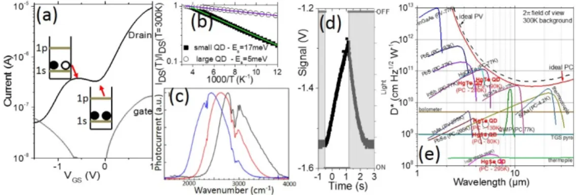
Figure

![Fig. 3. (a) Absorption spectra of HgSe CQD films with different surface chemistries, adapted with permission from [35], Copyright (2016) American Chemical Society](https://thumb-eu.123doks.com/thumbv2/123doknet/14394067.508756/8.918.255.670.390.604/absorption-different-chemistries-permission-copyright-american-chemical-society.webp)
![Fig. 5. (a) Infrared absorption spectrum of Ag2Se CQDs. (b) Absorption spectrum of Cr-Sn Doped In 2 O 3 CQDs, adapted with permission from [59], Copyright (2014) American Chemical Society](https://thumb-eu.123doks.com/thumbv2/123doknet/14394067.508756/10.918.248.665.308.496/infrared-absorption-spectrum-absorption-permission-copyright-american-chemical.webp)
Documents relatifs
Including Zeeman and exchange interaction terms in the Abragam-Pryce model we are able to interpret the differences between the g-values obtained by optical measurement and by
tion spectra has normally been made assuming purely sharp electronic levels (S.E.L.) and, therefore, neglecting the electron-lattice coupling, which gives. rise to more
OF the core electron with the spin upward, the exchange potential due to the hole is effective only on conduction electrons with the spin upward.. The exchange effect, of
ending at'ihe central photoabsorbing atom with n - l intermediate steps on the surrounding atoms, R P , indicates the corresponding total path length and the
This systematic investigation facili- tates the interpretation of the observed resonances and i s believed to help in the understanding of the chemi cal environment giving
A deconvolution procedure must be applied to the observed spectra which can be deeply distorted by the finite instrumental broadening.. Briefly, a syn- thetic spectrum of
Our measurements show a very small temperature dependence of the energy position of the dips in the whole range [4.2-300 K] and a small intensity of the dips,
Using additional data and an improved data analysis procedure, we have confirmed our recent observation of EXAFS in these molecules.. Results
