Design
and Analysis of a 200 Volt, High Slew Rate,
Current-Limited
Operational Amplifier
by Ignacio Estay Forno
S.B., Electrical Engineering, Massachusetts Institute of Technology, 2018
Submitted to the Department of Electrical Engineering and Computer Science in Partial Fulfillment of the Requirements for the Degree of
Master of Engineering in Electrical Engineering and Computer Science at the
Massachusetts Institute of Technology June 2019
c
2019 Ignacio Estay Forno. All rights reserved.
The author hereby grants to M.I.T. permission to reproduce and to distribute publicly paper and electronic copies of this thesis document in whole and in part in any medium
now known or hereafter created.
Author:
Department of Electrical Engineering and Computer Science May 24, 2019
Certified by:
Alec J. Poitzsch, Design Engineer, Thesis Supervisor May 24, 2019
Certified by:
Ruonan Han, Professor of Electrical Engineering, Thesis Supervisor May 24, 2019
Accepted by:
Design and Analysis of a 200 Volt, High Slew Rate,
Current-Limited Operational Amplifier
by Ignacio Estay Forno
Submitted to the Department of Electrical Engineering and Computer Science on May 24, 2019 in Partial Fulfillment of the Requirements for the Degree of Master of Engineering in
Electrical Engineering and Computer Science.
Abstract
This thesis is focused around the development of an amplifier with novel features in a 200 V silicon process internal to Analog Devices. Despite being on a closed-process, the discussion focuses on topological and architectural developments that are applicable to a wide range of high voltage processes.
The use case examined is one whereby large capacitive loads need to be driven by high voltage analog steps anywhere in a 200 V range, with ideal slew rates measuring in the kV/µs range, while having clean, adjustable current limiting and low quiescent current consumption. Several common amplifier topologies are examined, with their merits and drawbacks discussed in the context of the use case. Ultimately, a hybridized approach is taken for an input stage for the amplifier that accomplishes high slew rates at the output while maintaining accurate, adjustable current limiting.
The amplifier discussed, designed, and simulated operates at a 200 V rail-to-rail potential, with up to 1 A of continuous output current, with a slew rate exceeding 1 kV/µs, drawing only 25 mA quiescent, and user-adjustable current limiting that op-erates without the need for an inefficient in-line current-sense resistor. The current limiting blocks discussed operate with a no excess DC current or power to operate apart from a small amount supplied for current-limiting adjustability.
Thesis Advisor (Industry): Alec J. Poitzsch Title: Design Engineer, Analog Devices Inc.
Thesis Advisor (Faculty): Ruonan Han
Acknowledgements
First and foremost, I am deeply indebted to Alec. As my thesis advisor throughout my two rotations at ADI, Alec has been a great friend and mentor. In the future, I’ll look fondly at the whiteboard meetings wherein Alec would take time out of his day to sit down with me, one on one, and discuss circuit concepts and topologies with me until he was certain that I had acquired a complete grasp of the the material. It is at these meetings where my love of circuits was cemented into something that extended far beyond the scopes of a classroom or thesis topic. In these meetings I learned more than I could have learned under any amount of time spent poring over a book or other literature. I have to give a huge thanks to Alec, as through him, my fascination with integrated circuit design has grown and grown over time, to the point where I know with all of my being, that I want to make a career out of the field. Through Alec’s guidance, and the wonderful friendships with him and all of the other welcoming individuals at ADI, I truly found myself looking forward to every day where I would get to come in, be with friends, continue learning about circuits, and work on my projects.
I wish to also give thanks to professor Ruonan Han. Apart from being my faculty thesis advisor, a large bulk of my analog circuits courses throughout my time at MIT have been under professor Han in one way or another. In terms of breadth, as well as depth into the analog sphere of circuits, professor Han has had an undeniable impact on helping me learn and get to where I am today in terms of theoretical knowledge as it pertains to circuits. When it came time to pick a thesis advisor from the faculty, I knew without hesitation that I had to ask him first, and I still stand by that decision.
To my high school math and technology teacher, as well as robotics mentor, Mr. Evans, I wish to give a special thanks. To this day, I look back at my years in high school as the years where I settled in on electrical engineering as what I wished to study. Needless to say, I am grateful for the fact that, without him, I would almost certainly have majored and studied in a different field!
To Chris, Logan, and Patrick, I wish to thank for being the best friends anyone could ask for, the immense amount of emotional support throughout the years, and countless amount of memories we share across the past decade.
I’m thankful to the members of my family, for all their love and support, most of all my parents, for whom I wish to dedicate this thesis to. Without their unwavering support, this thesis would not have been possible. Through years of sacrifice and work, they’ve endeavored each and every day to give my sister and I the best lives we could possibly have. They’ve taken on the role of not just caretakers, but teachers and mentors over the years, instilling in me a sense of perseverance and diligence in the face of hardship, trouble, or challenge. In every step of the way, they’ve had my back, and done everything in their power to provide me with the strength to improve myself from a personal and professional standpoint. Their work ethic and selflessness is something that I try to emulate every day. I can only hope that they are as proud to have me as their son, as I am proud to have them as my parents.
Contents
1 Introduction 8
1.1 Motivation . . . 8
1.2 Design Goals . . . 11
1.3 Systematic Solution and Limitations . . . 12
2 Process 14 2.1 Devices . . . 15 2.1.1 HV LDMOS . . . 15 2.1.2 LV CMOS . . . 15 2.1.3 Zener Diodes . . . 16 2.1.4 LV BJT . . . 16
2.2 Design and Architecture Implications . . . 16
2.2.1 Gate-Source and Drain-Source Breakdown Considerations . . . 16
2.2.2 LV-HV Cascode Block . . . 17
3 Amplifier Building Blocks and Abstractions 19 3.1 Diamond Buffers . . . 19
3.1.1 Output Impedance . . . 21
3.1.2 Redirection of Current . . . 23
3.1.3 Input and Output Variations on the Diamond Buffer . . . 23
3.2 ZTAT Bias Cell . . . 24
3.3 Cascode-Propping Voltage Source . . . 26
3.4 Monticelli Bias Cell . . . 27
3.5 Mirrors . . . 29
4 Amplifier Architecture Considerations 31 4.1 Differential Pair Amplifier . . . 31
4.1.1 Slew Rate . . . 32
4.1.2 Current Limiting . . . 34
4.2 H-Bridge Amplifier . . . 36
4.2.1 Slew Rate . . . 37
4.2.2 Current Limiting . . . 37
5 Hybrid-Input-Stage, High Slew Amplifier 40
5.1 Input Stage . . . 40
5.2 Rail-to-rail Output Predriver . . . 41
5.3 Output Buffer . . . 42
5.4 Current Limiting . . . 44
5.4.1 Indirect Current Sampling via Mirroring . . . 45
5.4.2 Current Comparator and Adjustable Current Limiting . . . 48
5.4.3 Regimes of Operation . . . 50
5.4.4 Output Buffer Clamp . . . 53
5.4.5 Input Buffer Deactivation . . . 54
5.4.6 Transmission Gates . . . 56
5.4.7 High-Z Gain Node Manipulation . . . 56
5.4.8 Solution Constraints . . . 58
5.4.9 Current and Power Overhead . . . 60
5.4.10 Footprint . . . 60
6 Simulation Results 62 6.1 Transient Behavior and Current Limiting . . . 63
6.1.1 Slew rate . . . 63
6.1.2 Current Limiting . . . 68
6.2 AC Behavior . . . 82
6.3 Monte Carlo Sizing Variation . . . 83
6.3.1 Input Offset . . . 83
6.3.2 Current Limiting Precision . . . 84
6.4 Temperature Dependence . . . 89
6.4.1 ZTAT Current Source . . . 89
6.4.2 Input Offset . . . 90
List of Figures
1.1 AMOLED Pixel Subassembly. . . 9
1.2 Example of an AMOLED matrix with independent gate drive and column drive. 10 1.3 System-level solution for low voltage operational amplifier running on high voltage bootstrapped supplies . . . 13
2.1 Protection circuitry for n-type devices using Zener diodes . . . 17
2.2 LV common-source stage (left) and LV-HV cascode (right) . . . 18
3.1 4-Transistor Diamond Buffer . . . 20
3.2 Diamond Buffer Currents Offset from Input . . . 22
3.3 ZTAT bias cell . . . 24
3.4 VGS multiplier voltage source . . . 26
3.5 Rail-to-Rail output stage with Monticelli Cell, and Abstraction . . . 29
3.6 Cascoded Current Mirror (left) and Abstracted Symbol (right) . . . 30
4.1 Rail-to-Rail Dual-Differential Pair Amplifier. . . 31
4.2 Simplified Block Diagram of LT1970 Source-Side Current Limiting Circuitry 35 4.3 Rail-to-Rail H-Bridge Amplifier. . . 36
4.4 Simplified Hybrid Input Stage Amplifier . . . 39
5.1 Input Stage for Hybrid Amplifier . . . 41
5.2 Rail to rail predriver with Monticelli cell for DC bias . . . 42
5.3 High current drive output buffer . . . 44
5.4 Typical current sensing solutions . . . 45
5.5 Regulated cascode current mirror for sink-side output indirect sensing with gain of 1/20 . . . 48
5.6 Source-side output current comparator circuit with adjustable preload com-parison current . . . 50
5.7 Plot of different current-limiting regimes that the amplifier can inhabit . . . 52
5.8 Output buffer shutoff circuit for source-side current limiting . . . 53
5.9 Input buffer shutoff circuit . . . 55
5.10 High-Z gain node manipulation for source-side limiting . . . 57
5.11 Non-monotonic load I-V characteristic for first quadrant . . . 59
6.1 160 VP P square wave to illustrate slew rate in current limited (amber) and non-limited (green) amplifiers with no load . . . 63
6.3 Zoomed-in version of figure 6.1 to illustrate downwards slew . . . 65
6.4 Zoomed-in version of figure 6.1 to illustrate upwards overshoot . . . 67
6.5 Zoomed-in version of figure 6.1 to illustrate downwards overshoot . . . 67
6.6 Current limited output of a sinusoidal current signal . . . 69
6.7 Zoomed-in plot from figure 6.6 to illustrate regime shift . . . 69
6.8 Current limiting of a sine wave at 125 mA increments . . . 71
6.9 Current limited sinusoid at different process speeds . . . 72
6.10 Zoomed-in plot from figure 6.9 . . . 72
6.11 Current limited sinusoid at different temperatures . . . 74
6.12 Zoomed-in plot from figure 6.11 . . . 74
6.13 Current limited output of an analog step current signal . . . 76
6.14 Zoomed-in plot from figure 6.13 to illustrate step response . . . 76
6.15 Current limiting of a square wave at 125 mA increments . . . 78
6.16 Zoomed-in plot from figure 6.15 . . . 78
6.17 Current limited step response at different process speeds . . . 79
6.18 Zoomed-in plot from figure 6.17 . . . 79
6.19 Current limited step response at different temperatures . . . 80
6.20 Zoomed-in plot from figure 6.19 . . . 80
6.21 Further zoomed-in plot from figure 6.20 . . . 81
6.22 Gain and phase characteristics with annotated properties . . . 82
6.23 Histogram of input-referred offset voltages from 1000 Monte Carlo simulations 83 6.24 Distribution of current limiting with no preload. µ = 71.8mA, σ = 1.36mA . 84 6.25 Distribution of current limiting with preload set for limiting at 500 mA. µ = 500mA, σ = 1.68mA . . . 85
6.26 Distribution of current limiting with preload set for limiting at 1000 mA. µ = 1000mA, σ = 2.53mA . . . 85
6.27 Current limiting precision of 10 random Monte Carlo samples across temper-ature with 0 preload. . . 86
6.28 Current limiting precision of 10 random Monte Carlo samples across temper-ature with preload set for 500 mA. . . 87
6.29 Untrimmed vs single-point-trimmed temperature dependent drift sweeps for the same 10 random Monte Carlo samples . . . 88
6.30 Temperature-independent current source across wide range of operating tem-peratures . . . 89
6.31 Systematic input-referred offset drift across wide range of operating temper-atures . . . 90
Chapter 1
Introduction
1.1
Motivation
In the past decade, and for the foreseeable future, AMOLED (Active Matrix Organic Light-Emitting Diode) displays have been increasingly used in consumer electronics, with adoption increasing substantially in the market set to only increase in size [1]. Modern AMOLED displays work by pairs of transistors and a capacitor working together in order to power individual LED sub-pixels [2] on a thin film transistor (commonly referred to as TFT) array. Figure 1.1 displays a typical schematic for an OLED pixel subassembly.
Figure 1.1: AMOLED Pixel Subassembly.
During an update event, the gate drive input will be activated, forcing MP1 to conduct, charging MP2 and the associated capacitor to whatever value corresponding to the data sent by the column drive bus. This value is held by the capacitor once the gate drive connection is deactivated, and changes to the new column drive (data) value the next time the gate drive connection is activated. Figure 1.2 displays how, through this context, a grid of n · m of these subassemblies, can be controlled by n Gate drive channels and m column drive channels. Pixel data for a row is written to the column drive channels, and then the column drive channel corresponding to the row is driven, charging up the row of pixels with their respective values.
Figure 1.2: Example of an AMOLED matrix with independent gate drive and column drive.
One property of AMOLED panels is their tendency to “burn-in,” or have their luminance figures fade throughout the panel’s lifetime. Through manufacturing imperfections, two sep-arate panels may not necessarily have the same luminance right after production, and one may be “pre-burned” compared to another. In order to ensure consistency across different panels and devices, original equipment manufacturers will typically age panels until they are equally luminant. Aging involves sending sequences of sharp, high slew rate analog steps to activate and deactivate portions of the display in as controlled a manner as possible.
The panels undergo aging before they are cut up into their final-use size. As a result, the circuitry driving the row scan lines and the column data lines will be seeing large capacitive loads proportional to the dimensions of the panel as a whole. Thus, an ideal device to act as a buffer driving these lines would have low output impedance, a high range of output voltage, controllable slew rates, and some form of adjustable current limiting to work well under a wide array of different loads.
The purpose of this thesis will be to examine different pre-existing amplifier architectures and design methodologies to evaluate their aptness for the use case presented. Additionally, we wish to present and analyze a novel integrated circuit architecture for an IC-level design that is well-suited to this use case. The proposed architecture should be able to serve as an all-in-one amplifier and output driver, as opposed to system-level solutions that rely on separate, discrete components.
1.2
Design Goals
Based on the presented use case we can compile a list of desired specifications for the am-plifier discussed.
Specification Value
Output Voltage 200 V, ± 100 V
Slew Rate ≥ 1 kV/µs
Unity Gain Frequency MHz Range
DC Current Consumption ≤ 30 mA
Output Current 1000 mA continuous
Output Current Limiting Adjustable on range (500mA, 1000mA) Table 1.1: Desired Specifications
1.3
Systematic Solution and Limitations
Oftentimes, a monolithic amplifier capable of withstanding high operating voltages will not be available for use, as high-voltage solutions and processes are still a developing sector in the IC market. A common workaround to this issue is utilizing a bootstrapping technique whereby the output of a low voltage amplifier is connected by means of a step-up and a step-down voltage source into the gate of complementary high voltage devices that act as source followers, providing power rails for the amplifier that track the output and allow the output of the system to have a voltage swing much wider than the monolithic amplifier on its own. Figure 1.3 displays an example of a low voltage operational amplifier being used in such a configuration. In this instance, voltage sources (implemented as diostacked de-vices, or resistors) serve to give headroom on top-side and bottom-side connections that feed into high voltage devices (marked as HV) that can withstand large VDS values, providing
power rails to the amplifier referenced to its output. These power rails for the amplifier will follow the output of the amplifier and can allow an increased window of output operating voltages.
The key benefit that the systematic solutions have over a monolithic solution lies in power density with respect to area. In a monolithic solution, the die is responsible for sustaining the entire potential, with all of the quiescent power used being dissipated into the substrate as heat. In the case of a system-level solution attempting to operate at high voltages, the (low-voltage) amplifier itself would only dissipate power corresponding to its quiescent cur-rent times its power supply operating voltage. The curcur-rent would be redirected through the HV external devices that would bear the brunt of the quiescent power consumption. The sep-arate power dissipation across the different physical components allows for the amplifier to operate at a lower temperature (where it can operate at higher performance and efficiency), and allows for the majority of the heat to be dissipated through the external high-voltage devices, for which heat sink solutions are prominent and abundant on the market.
Figure 1.3: System-level solution for low voltage operational amplifier running on high volt-age bootstrapped supplies
Issues, however, exist with this systematic approach to the issue. First and foremost, this approach requires more physical components than a monolithic solution. In this partic-ular use case, two high voltage MOS devices, two external voltage sources (composed of diode-connected transistors, or resistors), and two external resistors, are needed in order to implement the setup. By comparison, a monolithic solution would not have the drawbacks of extra board space used by external devices. Furthermore, if such a design is to be used, the system must be designed such that the inputs will always be within the operating range of the variable supply rails supplied by the high voltage MOS devices. An alternative to this is to use an amplifier with over-the-top or under-the-bottom functionality at the in-puts. Regardless of the method used to preserve input integrity throughout the operating range, these limitations are still in place and hinder a multitude of applications. It is when these limitations are laid out that the need for a monolithic, high voltage solution becomes apparent.
Chapter 2
Process
Of particular interest and difficulty in this thesis will be the specific process technology being used. This process allows for the amplifier being designed to withstand the full range of 200 V from one supply to another. Within the BCDMOS (Bipolar, Complementary, Depletion, Metal-Oxide-Semiconductor) process being used, only certain devices are able to withstand the 200 V, potential across the drain-source channel. Additionally, no devices are capable of more than several volts across the gate-source terminals. The high-voltage devices involved in breaching the 200 V jumps in potential are also limited in their performance specifications compared to the low-voltage devices, having worse DC gain, higher parasitic capacitances, and worse high-frequency performance.
Due to these limitations, much of the design work done will be centered around the use of cascode cells within the amplifier to combine the high performance metrics of the low-voltage devices with the resilience of the high-voltage devices.
2.1
Devices
2.1.1
HV LDMOS
The high voltage LDMOS (Laterally-Diffused Metal-Oxide-Semiconductor) transistors are the primary device used in interfacing with voltage nodes that will have swing up to the entire 200 V range specified for the amplifier. There are several characteristics of these LD-MOS devices relevant to the project as a whole.
First and foremost, the LDMOS devices have the ability to sustain high VDS values on the
order of 200 V without experiencing breakdown. The LDMOS devices are capable of with-standing high potential across their nodes in part due to the large, spaced-out geometry (particularly length) that prevents electric fields from growing large enough in magnitude to cause breakdown. As a consequence of this expanded geometry, the small-signal gate-source capacitance, Cgs, of the devices will be relatively large and transconductance, gm, relatively
small in comparison to a traditional micron or sub-micron low voltage MOS device. As transition frequency, fT, is a function of fT = 2π(Cgsgm+C
gd), the high voltage devices will have
significantly reduced bandwidth in comparison to a smaller, low voltage device.
2.1.2
LV CMOS
Within the process being used, traditional micron-scale CMOS (Complementary Metal-Oxide-Semiconductor) devices are available. These function as standard CMOS devices and are operated at VGS and VDS values of 5 V or less.
2.1.3
Zener Diodes
Zener diodes are used throughout the circuit primarily as a protective device. Their forward voltage drop of 0.6 V and reverse bias drop of approximately 5 V are useful to prevent reverse biasing and device gate breakdown, respectively.
2.1.4
LV BJT
Low voltage BJT (Bipolar Junction Transistor) devices, though not used extensively within the signal chain of the amplifier, are used in the ZTAT bias cell due to their well-documented behavior across temperature, allowing for temperature-independent currents to be generated in order to bias the amplifier as a whole.
2.2
Design and Architecture Implications
2.2.1
Gate-Source and Drain-Source Breakdown Considerations
Due to the nature of the design blocks and topologies being used, many nodes within the amplifier(s) discussed, especially high-Z nodes, will be susceptible to large swings in voltage. Oftentimes, these nodes will be used to drive gates of gain-stage low voltage and high volt-age devices. In either case, the VGS of such a device cannot experience more than roughly5 V of potential difference before experiencing gate breakdown. In order to protect devices from a breakdown event, Zener diodes are placed parallel to gate-source connections. The asymmetric I-V behavior of the Zener diode also prevents reverse-biasing of the VGS value
for devices. In the case of the low voltage devices, Zener diodes are also placed parallel to the Drain-Source channel to prevent VDS breakdown as well as reverse-biasing of the channel.
Figure 2.1 displays the style of protection used in low voltage and high voltage n-type de-vices. P-type devices are protected using a similar, but complementary, topology. Through-out the circuits discussed in the thesis, devices are implied as having these Zener protections in place. Their absence in figures is a deliberate choice to simplify and de-clutter schematics.
Figure 2.1: Protection circuitry for n-type devices using Zener diodes
2.2.2
LV-HV Cascode Block
As a consequence of the poor gmand fT characteristics of the high voltage devices, a common
design tool employed is a cascode block with a low voltage device being the ”current-setting” device, with a high voltage device in series with it. An example setup is displayed in figure 2.2. The benefit of such a configuration is that the topology allows for the high voltage de-vice to bear the brunt of the high-swing node at its drain-source channel, ensuring that the low voltage device does not see more than (VGS,LV + Vprop) − VGS,HV across its channel. The
value of Vprop is chosen such that the low voltage device does not experience breakdown
Chapter 3
Amplifier Building Blocks and
Abstractions
Throughout the amplifier as a whole, many sub-circuits work together in order to meet performance specifications. In order to ensure understanding, this chapter is a legend of sorts, to provide important information on the makeup of the circuit blocks and abstractions used throughout the thesis.
3.1
Diamond Buffers
”Diamond”-style buffers are used at both the input and output of the amplifiers discussed in this thesis. In each situation, they take a high-impedance voltage-mode signal and buffer it to their low-impedance output. Their output leg also serves as a robust current buffer, useful for redirection, mirroring, and measurement. The amplifier discussed in this thesis uses a variation on what is commonly referred to as a diamond buffer used in bipolar processes, though the method of operation is similar. Despite bearing the same name, the topologies are slightly different. The topology for the diamonds discussed in this thesis is that of the one in figure 3.1.
The mode of operation of the diamond buffers used in this work is equivalent to that of a typical Class AB output stage biased with like-to-like diode-connected devices. In figure 3.1 (Note that this figure only shows high voltage devices, whereas typically a LV-HV cascode is used when implementing the block into an amplifier), the input is fed into a high-impedance node, where current sources direct current through diode-connected devices, MNI and MPI, creating VGS values corresponding to the current density through the devices. These VGS
values prop up the gates of output devices, MNO and MPO, with an effective VGGO = 2·VGS.
If input and output devices are matched in length, then if all devices have sufficient VDS to
remain in saturation, then the output devices will retain the same current density as the input devices when under no load or offset between input and output.
3.1.1
Output Impedance
The buffer output can be driven in 2 different types of regimes. Figure 3.2 displays the differ-ent modes of operation as they pertain to currdiffer-ents within the output devices and the output of the buffer as a whole. For simplicity, this graph assumes a VT of 1 V for both output
devices, and identical k0 WL values. The first mode of operation when the buffer operates in Class AB operation. Under this mode, both output devices have VGS ≥ VT. As output
volt-age offset from the input shifts below the input, the current through device MNO increases proportional to (VGS,n− VT)2, and the current through MPO decreases following the similar,
complementary behavior. Through this unbalanced change in currents, plus KCL, the result is that the buffer will source more current through the output node (IBuf f er,Out < 0). As
output voltage with respect to input voltage decreases further, the VGS of MPO will decrease
sufficiently such that MPO will enter its shutoff regime and the buffer will only have MNO supplying all of the current.
Figure 3.2: Diamond Buffer Currents Offset from Input
With regards to output impedance, the small-signal conductivity can be well-modelled as ZBuf f er,Out = 2g1m. Around the zero-offset point, this value remains fairly linear in slope,
however after one device enters shutoff, the quadratic behavior of the on-biased device will dominate, and its transconductance will increase, thereby decreasing the output impedance, and increasing current driving capability. This fact can be leveraged to have small-signal stability for small-signals, but also vast current-driving capability for large-scale signals.
3.1.2
Redirection of Current
In the buffer discussed, especially in large signal scenarios when one of the output devices, MNO or MPO, are in shutoff, the entirety of the current being sourced or sunk through the buffer’s output will be directed through the complementary device, MPO and MNO respectively. This current can be mirrored and used elsewhere in the amplifier for gain stages or measurement.
3.1.3
Input and Output Variations on the Diamond Buffer
These style buffers are used in both input and output stages in several of the amplifiers discussed in this thesis. Their topology in each case is nearly identical, the key difference being that the output stage buffer is sized up significantly to be able to drive up to 1 A of current continuously without breakdown.
In each case within the amplifier, the main difference from the block in figure 3.1 is that a LV-HV cascode is used for the buffer outputs in order to have the high-speed, matching, and precision characteristics of low voltage devices while having the operating range of high voltage devices. This is particularly important in the diamond buffers used within input stages, as cascode blocks allow for lower offset from buffer inputs to buffer outputs, which can manifest itself in lower input-referred voltage offset for the amplifier. Additionally, low voltage devices in the process are easier to interleave in layout compared to high voltage devices, which can further reduce process mismatch-based input referred offset.
3.2
ZTAT Bias Cell
Figure 3.3: ZTAT bias cell
The proposed monolithic amplifier will have a standby thermal power dissipation on the order of 10s of Watts, with higher power dissipation expected when put under load. Due to this highly-variable, dynamic power dissipation within the amplifier as a whole, the tem-perature of the die is reasonably expected to vary significantly over time. In order to have consistent operation and biasing of devices within the amplifier, a temperature-independent source is required.
Figure 3.3 displays a bias cell with a central mode of operation similar to that of a Brokaw-style bandgap source [6]. There are several ways in which this implementation varies com-pared to the typical bandgap reference. These modifications deal with stability, start-up
self-biasing, high-voltage operation, matching, and over-current protection.
• In figure 3.3, CComp is placed in such a way to take advantage of the Miller effect in
order to maintain stability of the biasing throughout the ZTAT cell [7].
• Rstart is placed and sized such that it will produce sufficient trickle current to bring
the self-biasing ZTAT cell into the ”on” self-biasing stable point.
• The high voltage LDMOS device in line with the output, marked ”HV,” is used as the top device in the LV-HV cascode in line with the output ZTAT current. The HV device insulates the LV device it is in line with and allows the output to as high as 200 V above the VSS rail
• Resistor RAB−M atch is sized such that when the circuit as a whole is under the ZTAT
operating point, the resistor will have a ZTAT current directly proportional to the output current running through it. From current running through the resistor, the potential at the gate of the high voltage LDMOS output device can be set higher or lower, acting as a source-follower, setting VB to be
VB = VDD,LV − IAB−M atch· RAB−M atch− VGS,HV. (3.1)
Given this equation, RAB−M atch can be set such that VB = VA, improving the
accu-racy of the current mirror that sets the output ZTAT current. This resistor can be implemented as an external resistor to allow for bias cell trim, and remove its resis-tance from the rapid temperature fluctuations that can be expected on the die itself. Alternatively, this resistor can also be set as a short internally or externally, providing a cascode for which the output leg can interface with high voltage.
• As the low voltage supplies, VDD,LV and VSS,LV, are pulled apart during turn-on of
the self-biasing portion of the ZTAT cell to experience temporary surge currents many times larger than the intended ZTAT current. Under these conditions, the current is mirrored through RAB−M atch, at which point the potential at the gate of the high
voltage LDMOS output device is brought down closer to the VSS rail. Lowering this
potential greatly limits, or even shuts off, the output current sent to the rest of the circuit as a whole. This protects the amplifier from seeing greatly increased shoot-through current turn-on that could damage biasing circuitry.
3.3
Cascode-Propping Voltage Source
Figure 3.4: VGS multiplier voltage source
A key building block used in the construction of several cascodes in the amplifier is the VGS
multiplier voltage source. In figure 3.4, a low voltage device has two resistors in parallel with its channel, a node between them connected to the gate of the device. When biased with sufficient current, the transistor in the block enters a stable state where it reaches saturation, with an associated VGS forming across RGS. From Ohm’s law, this potential difference has
a corresponding current, IR= RVGS
GS. As current cannot flow through the MOSFET’s gate, it
flows through RDG, creating a potential, VDG = IR· RDG. Substituting in for IR, we arrive
at VDG = RVGS
GS · RDG. Thus, we have VDS = VDG+ VGS =
VGS
to VDS = VGS· (1 + RRDG
GS). Based on the ratio between the resistors listed, such a setup can
be used to create an arbitrarily chosen potential anywhere where a current can be channeled through. In the amplifier, this typically presents itself as a Vprop as seen in figure 2.2. Low
voltage n-type devices are used for these VGS multipliers due to their superior high-frequency
response compared to high voltage devices.
3.4
Monticelli Bias Cell
Common issues to deal with in two-stage rail-to-rail output operation amplifiers are that, there is often not anything setting the DC bias point for the output leg devices, and that there is little-to-nothing stopping differential-mode current signals to enter in through n-side and p-side inputs, potentially leading to out-of-control current growth or shrinkage at the output leg. The circuit block displayed in figure 3.5 serves to mitigate any differential mode input error to an output predriver as well as set the DC current level in the predriver’s output leg.
The bias current displayed, IBias, serves to create potential VM N 4,G = 2VGS above the bottom
rail. This node is connected to the gate of device MN5, which serves as a source follower buffering to the gate of MN0 and the drain of MN2 and MN3. If configured properly, current densities among all the legs in the circuit should be identical, resulting in MNO to have a VGS,M N 0 that lines up almost exactly to the VGS,M N 1 generated by a fixed IBias. This sets
the DC operating condition of the output leg and allows for fine-tuned control of the current density.
In the case where such a block is not put together with a typical rail-to-rail output stage, there is no connecting path between the gate of the device MNO and gate of the device MPO. As a consequence of this, if any upstream circuitry were to send a differential amount
of current into the different input legs, the gates would not track each other. Take, for exam-ple, a positive current going into the n-side input of the rail-to-rail output stage, but not the p-side input, then the potential at the gate of MNO would quickly rise, causing MNO to sink more current, without reducing the current drive supplied by MPO. This would increase the current and power consumed by the amplifier’s output stage, bring the output node down to near-VSS,HV, and degrade performance. The displayed block solves this issue, primarily
by ”linking” the gates of MNO and MPO through the channels of devices MN5 and MP5. In the same case of deferentially high current being sourced to the n-side input, MN5 would act as a common-gate current buffer, bringing any extra current up to the node connected to the p-side input as well. This would force both nodes to move together and only ”see” effective common-mode inputs across the gates of MN0 and MP0.
This circuit block is referred to as a Monticelli Cell, after Dennis M. Monticelli’s disclosure of the technique in his patent, ”Class AB Output Circuit with Large Swing,” in US Patent 4,570,128 [8]. This particular implementation differs from Monticelli’s original work in that his original cell had solely a single input, whereas this topology is double-sided, with p-side and n-side inputs to match the complementary nature of the rest of the amplifier’s topology.
Figure 3.5: Rail-to-Rail output stage with Monticelli Cell, and Abstraction
3.5
Mirrors
Used throughout the circuit in places such as bias stages, gain stages, and shutdown circuitry are current mirrors that redirect, amplify, or attenuate current-mode signals. Typically, they are implemented as a LV-HV cascode for improved output resistance, and wide voltage swing capability at the output. In diagrams and schematics, a mirror will typically be drawn as a box with a curved arrow, as in figure 3.6. In cases where there is no 1:N ratio explicitly stated on the mirror, it can be assumed that it is a 1:1 mirror.
The stacked topology is used as opposed to a traditional high-swing MOS cascode mirror, as neither input nor output headroom are not crucial properties in the applications discussed, and a 1:1 exact LV-to-LV and HV-to-HV arrangement is more easily controlled across pro-cess variation and temperature shifts.
Chapter 4
Amplifier Architecture Considerations
4.1
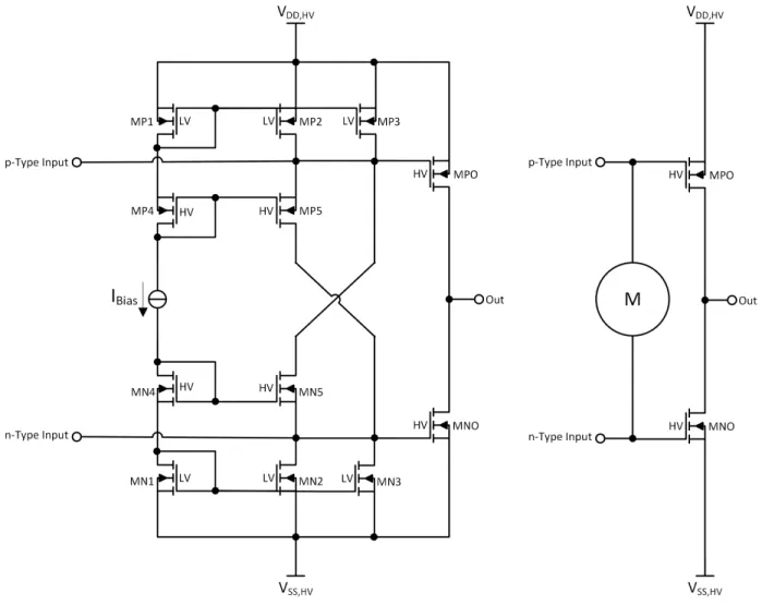
Differential Pair Amplifier
As a base case, it is helpful to examine a traditional, two-stage amplifier based on differential pair inputs. In figure 4.1, a rail-to-rail output, two-stage amplifier with Monticelli cell, is displayed. The displayed amplifier consists of two differential pair input stages, placed against their own respective mirror stages, feeding into gates of the n-type and p-type output devices. The input stages are biased with fixed tail currents, supplied by IT ail.
4.1.1
Slew Rate
An area in which the differential pair amplifier encounters significant limitation is in output slew rate. With a differential pair amplifier, a maximum slew case would be one in which almost the entirety of the tail current, IT ail, is redirected through one of the two input
de-vices each, on the n-type and p-type input sides.
In the case of the amplifier in figure 4.1, one possible full-slew case would be the one in which the non-inverting input, V +, is significantly above the inverting input, V −. In this situation, the n-type input stage has device MNP fully active and MNN fully in shutoff, whereas the p-type input has MPN fully active, and MPP in shutoff.
As MNN and MPP are both in shutoff, the entirety of their DC bias current, IT ail, is
trans-mitted through MNP and MPN. On the n-type(p-type) input, the top-side(bottom-side) current mirror mirrors the zero(full) current across to its output. Since the full brunt of IT ail is still traversing through MNP(MPN), with MNN(MPP) taking zero, all of the current
must come from node VG,T op(VG,Bot). In both cases, IT ail is being sourced from the VG nodes,
in which case the resultant shifts in potential will be common-mode, and the Monticelli cell will not have any effect. This leaves the capacitive load of the output device gates, as well as the compensation capacitors, Cc,p and Cc,n, which are tied to the output node. In this
example, both compensation capacitors are identical in capacitance. Sized to properly com-pensate the amplifier, the capacitance due to compensation devices will be significantly larger
than the capacitance presented by the output device gates. As such, it is acceptable in this case to approximate the load to be primarily capacitive with it being tied to the output node.
The rate of change of voltage across a capacitor can be modeled as
dVC
dt = IC
C, (4.1)
with VC representing voltage across the capacitor and IC representing current flow through it.
Because nodes VG,T op and VG,Bot are both high-impedance nodes tied to each other through
the Monticelli cell, the differential voltage across the compensation capacitors occurs at the output node. As a result, the maximum output slew rate of an amplifier such as the one in figure 4.1 becomes dVout dt = IT ail,p+ IT ail,n Cc,p+ Cc,n = 2 · IT ail 2 · Cc = IT ail Cc . (4.2)
Given this relationship, there are two main methods by which the slew rate of the amplifier can be improved without modifying the amplifier topology. The first method is by decreasing the size of the compensation capacitors. As the compensation capacitors are already sized such that they will provide proper stability for the amplifier, this is not possible without doing a complete rework of the amplifier. The other option is to increase the DC tail current to a higher value, such that the compensation capacitors can charge or discharge more quickly, resulting in higher output slew rates. Scaling the tail current up, however, poses issues. Take, for example, a differential pair amplifier using a 5 pF compensation capacitor. In order to reach a slew rate of 1 kV/µs with this amplifier, an IT ail value of 5 mA would
be required. If operating at 200 V, each mA unit of current consumption corresponds to a 0.2 W power consumption. In the DC case, increasing the power by the order of watts can rapidly heat up the die on which the part sits, degrade individual device performance, and quickly overrun the thermal limitations of the process, potentially leading to permanent part
damage, or thermal shutoff.
4.1.2
Current Limiting
Current limiting in the case of a differential pair amplifier with a fixed tail current can be accomplished efficiently by interrupting the signal path to modulate the output to a value that reduces the current output to a desired value. The LT1970 is a basic power operational amplifier commonly used in applications such as DIY adjustable bench top power supplies. Part of its allure in this market is its accurate current sensing and limiting, which works based off of interrupting and overpowering its own signal chain in the case of an over-current condi-tion [9]. If the amplifier is sourcing too much current (as determined by a user-configurable voltage mode pin, V CSRC), then current-limiting circuitry will pull on the high-impedance
input-side of the output buffer, fighting against its input gain stage, to pull the amplifier output down until the output current does not exceed the desired maximum current as deter-mined by the user. A simplified block diagram of the current limiting circuitry on the LT1970 is displayed in figure 4.2. In using a method such as this, the current-limiting signal chain interruption circuitry only needs to be powerful enough (from a current drive perspective) to overpower current-mode signals from the input stage operating on the high-impedance node. This lends itself well to a fixed tail current amplifier, as the footprint of the limiting circuitry can be similarly sized to that of the input stage.
In the case of the LT1970, the high-impedance node that is manipulated to perform limiting feeds into an output buffer. In the case of the amplifier displayed in figure 4.1, the input stage drives a high-impedance node feeding into an inverting gain stage at the output. The current-limiting implementation for such an amplifier is similar in function to that of the LT1970, but polarized oppositely to compensate for the inverting gain output stage. In the case where the amplifier would be sourcing too much current, limiting circuitry could work based on sinking current into nodes VG,T op and VG,Bot. If the current sunk into these nodes is
equal to or greater than the current sourced from them, IT ail, then the voltage at these nodes
will begin to rise, pulling the gates of output devices MNO and MPO upwards, causing the amplifier’s output voltage to lower until the current being sourced by the amplifier decreases to a level where it does not trigger current limiting.
4.2
H-Bridge Amplifier
Figure 4.3: Rail-to-Rail H-Bridge Amplifier.
A variation on the traditional two-stage operational amplifier uses an input stage built around the use of two diamond buffers rather than differential pairs. Figure 4.3 displays a simplified block-schematic of such an amplifier utilizing diamond buffers. This input architecture is typically referred to as an H-bridge input, for the topological shape formed by the diamond buffers and their supply legs. When a differential input is supplied, the diamond buffer inputs buffer the voltage-mode signal across a gm resistor, Rgm. This differential voltage across the
gm resistor causes a current to flow through, which is redirected through the supply legs of
each buffer, and sunk either directly into the high-impedance gates of the output devices, or into the gain mirrors above and below the buffers, which mirror the signal over into the complementary gate nodes.
4.2.1
Slew Rate
One area in which the H-bridge architecture is very effective in is in slew rate applications. Unlike a fixed tail current differential pair amplifier, the signal currents in an H-bridge amplifier are not a fixed multiple of the DC bias currents, rather they scale up quadratically with respect to the offset from the buffer inputs to their outputs. In the case of having near-ideal buffers, the gm resistor becomes the dominant limiter of the small-signal gm of
the input stage. However, in large-signal scenarios (neglecting ESD clamp diodes typically placed across the input terminals), the signal current can scale up over an order of magnitude above their DC levels. As there is no hard limit on what current can charge or discharge compensation capacitors, there’s no hard limit on the slew rate of an amplifier using such an input stage.
4.2.2
Current Limiting
The same attribute that makes an H-bridge input stage suitable for high-slew applications makes it difficult to work with in current limiting applications. In a traditional differential pair style amplifier, any feedback current limiting circuitry (such as the one in figure 4.2) would only need to supply enough current to fight the pre-determined IT ail. In the case of an
H-bridge input stage amplifier, as the limiting circuitry would pull the high-impedance node in the direction opposite to that being driven by the input stage, the output of the amplifier would be pulled away from its value were it to be an ideal operational amplifier given the feedback system in which the amplifier is placed. This, in turn, would pull the inputs apart from each other, leading to ever-increasing currents generated by the H-bridge input stage, which would fight against the limiting circuitry.
The end result of this increasing-currents-fighting-increasing-currents is that, although lim-iting is possible, it requires having the limlim-iting circuitry ramp up to and overpower the maximum-slew case. This would manifest itself as a constant magnified power consumption
within the amplifier during limiting scenarios, thereby heating the devices involved. This would perhaps be acceptable in cases where the limiting is being used as a short-circuit prevention mechanism, but if the limiting is to be used in a high-duty-cycle or accuracy-dependent application, this is solution would be both inefficient and inaccurate due to the wildly shifting die temperature.
4.3
A Hybrid Approach to Input Architecture
Given the limitations of the purely H-bridge or purely differential pair input stages as they pertain to slew rate or current limiting, it becomes apparent that neither topology is sufficient for both of the applications. Consequently, one possible solution is to utilize a hybridized architecture that exhibits the best of both worlds when it comes to current limiting and slew rate applications.
One possible hybridized implementation is displayed in figure 4.4. In this implementation, the two types of input stages are in parallel with each other. The differential pair input stage operates normally, being active regardless of current output condition. The H-bridge part of the amplifier operates selectively dependent on the output current condition. Under current output below that deemed to be over a preset limit, the switches connecting the buffers to the gm resistor are closed, allowing current to flow and boost slew rates to traditional
H-bridge levels. Under an over-current case, the switches connecting the buffers to the gm
resistor can be opened, cutting off the path by which the H-bridge increases signal current. Under this switch-open condition, the circuit is then controllable in a current limiting sense just as a traditional differential pair amplifier could be controlled.
Chapter 5
Hybrid-Input-Stage, High Slew
Amplifier
The amplifier as a whole is based on an architecture not unlike that discussed in figure 4.4 (For a more detailed overview of the amplifier schematic, see appendix figure 7.1)
5.1
Input Stage
Central to the slew and current limiting capabilities of the amplifier presented is the hy-bridized input architecture. Figure 5.1 displays the transistor-level topology of how the input stage is configured. Of particular interest is the use of transmission gates in line with the path of the diamond buffers. Under normal operation, the connections to the trans-mission gates (shown as switches in the figure) are a diode drop above the potential of the diamond buffer’s output. This effectively shorts the output nodes of the diamond buffers to each other, allowing for high slew rates under normal operation.
In parallel with the H-bridge portion of the input stage are two differential pairs biased with weak tail currents, of n-type and p-type respectively. These differential pairs are constructed of low-voltage primary devices with their gates tied directly to the amplifier inputs. The
differential pairs are equipped with high-voltage devices to create high-swing cascodes. This portion of the input stage operates regardless of whether the amplifier is in a current limiting mode, or a normal operating mode. Under normal operation, however, the bias currents are low enough such that the amplifier’s behavior is dominated by the H-bridge portion of the input stage.
Figure 5.1: Input Stage for Hybrid Amplifier
5.2
Rail-to-rail Output Predriver
The amplifier discussed uses a generic rail to rail output stage, utilizing LV-HV cascodes to drive the high-swing nodes of the output buffer. The DC current level of the predriver’s high-swing leg is set by the Monticelli cell in line with the low-voltage devices. One thing
to note is that the compensation capacitors present in this circuit block are inefficient with regards to physical layout space. As the nodes connected to the output buffer are high-swing nodes, able to swing the full 200 V between the supply rails, the capacitors must be special high voltage capacitors, that take substantially more surface area on the final die, as they must be made with far-apart metal layers rather than polysilicon layers.
Figure 5.2: Rail to rail predriver with Monticelli cell for DC bias
5.3
Output Buffer
A key requirement of the amplifier is the ability to drive high output currents on the order of 1 A continuously. Additionally, the amplifier must have a low-impedance output directly at the output node, before considering any feedback circuit. In order to fulfill these
require-ments, a LV-HV cascode diamond buffer is used at the output of the amplifier. Due to the DC output current requirements, the size of the devices is scaled up. Sizing is chosen such that under a 1 A continuous load, the output leg devices are under half of their break-down current density. This safety factor of 2 ensures that under high-slew scenarios, where temporarily increased shoot-through current occurs in the output leg, devices do not break down. Additionally, the larger-sized devices help spread heat across twice the area on the die, slightly diminishing the strength of temperature gradients across the device.
For the output buffer, a LV-HV cascode is used, with low voltage devices being used as the interface to the output for their better gm characteristic, and their resistance to breakdown
during any potential shoot-through current in the input and output legs during high-slew events. In layout, high voltage and low voltage devices can be staggered so as to further spread heat on the physical die. The output buffer is the largest single circuit block in terms of physical area in the amplifier. The output leg of the output buffer is linked to a mirror array that handles the current-measuring and limiting circuitry.
Figure 5.3: High current drive output buffer
5.4
Current Limiting
The majority of the complexity present in the amplifier occurs within the current limiting cell and its connections to the rest of the amplifier. This subsection details all the individual means by which the amplifier accomplishes current limiting. In many cases, even a single one of the discussed subsystem signal paths will be sufficient to limit the current output of the amplifier. As configured, these subsystems all trigger together, helping to ensure both ro-bustness and consistency in the current limiting process across process corners, temperature, and desired current limiting level. All the subsystems discussed exist in a complementary fashion, in order to allow for sink-side and source-side current limiting.
5.4.1
Indirect Current Sampling via Mirroring
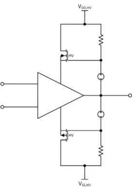
Traditionally, current sensing for an amplifier’s output is performed by nature of having a low-resistance sense resistor in-line with the output leg of an amplifier, or a similarly a small output resistor directly in line with the load itself. Figure 5.4 displays examples of output leg sensing and in-line sensing. This resistor then has the load current flowing through it, generating an associated voltage directly proportional to the output current. From here, this voltage (Absolute relative to a rail, or differential, depending on specific implementation) can be measured and used to calculate current flow, and henceforth implement a form of current limiting.
Figure 5.4: Typical current sensing solutions
In each of the traditional current sense application cases in figure 5.4, a singular resistor has to be capable of withstanding the entire brunt of the load current going through it. In the case of this amplifier’s use case, that would be up to an ampere of current in DC (and possibly more in a transient case). This presents several issues regarding physical space, manufacturing consistency, temperature independence, headroom, and dynamic range of limiting.
in DC.
• The resistor must be extremely consistent across process variation in its physical im-plementation.
• Due to the large currents being driven through it, and thus heat, the resistor must have a resistance very resilient to changes in temperature on the order of 100 ◦C or more.
• If the resistance of the resistor is too large, then under high current loads, an offset will grow between the direct output of the amplifier and the output to the load. This offset would restrict high-current output at voltages close to the rails of the amplifier.
• Any internal circuits measuring the voltage offset across the sense resistor would have to be physically small and operate under low DC power (as they would take the role of support circuitry). With these restrictions, their measurement accuracy (including factors like temperature and process variation) can only be on the order of about ±10 mV. If the headroom restriction is to be kept below 1V from each supply rail under maximum current load, then the largest value for the sense resistor is
RSense,M ax=
VSense
ILoad
= 1V
1A = 1Ω. (5.1)
With a voltage measurement accuracy of about 10 mV, this limits the current-limiting resolution to
IResolution =
VResolution
RSense
= 10mA. (5.2)
With a 10 mA minimum, and 1 A maximum current measurement, this gives only 2 decades of dynamic range.
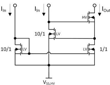
Due to the limitations of resistor-based current measurement, especially for on-die situations, an alternate method is explored in this implementation. One key thing to note is that, for current limiting applications, the exact magnitude of the current drive at the output is not a required piece of information. Realistically, it is sufficient to know if the current being driven is above or below a certain predefined threshold. Knowing this, it is possible to construct a limiting circuit that is triggered based off a current comparator. A regulated cascode is used due to its consistent current output characteristics across current densities, temperatures, and process variation, all while maintaining low input voltage headroom. Additionally, the high current gain accuracy allows for the regulated cascode mirror to be used without any degeneration resistors.
Use of a current comparator opens up the possibility for indirect sensing of the output cur-rent. With a low-operating-voltage current mirror placed in line with the output legs of the output buffer (See appendix figure 7.1), many of the limitations inherent to resistor-based measurement can be avoided. In the amplifier discussed, the output buffer is split up into 20 identical miniature buffers. Two of these miniature buffers have their supply rails sent through the inputs of a regulated cascode current mirror (pictured in figure 5.5) with an overall gain of 1/20 of the total mirror input current and 1/200 of the total amplifier output current. A regulated cascode mirror is used, as in the process it was more accurate across temperature and process variation compared to the LV-HV cascode mirrors used elsewhere in the amplifier. Additionally, the current measurement circuitry is not part of the direct signal chain of the amplifier, so the high-frequency poles introduced compared to a LV-HV cascode mirror are not an issue.
Figure 5.5: Regulated cascode current mirror for sink-side output indirect sensing with gain of 1/20
The other miniature buffers that are not mirrored over have their supply rails tied to diode-connected devices that set their effective supply voltage to a diode drop above or below the power rail. This condition allows all the miniature buffers to continue having near-identical supply behavior despite two of them being sent to a sampling mirror. With this countermeasure in place, the amplifier function is completely unaffected by the mirroring and limiting circuitry when the current limiting is not triggered.
5.4.2
Current Comparator and Adjustable Current Limiting
A key feature of the proposed amplifier is that the current-limiting circuitry is capable of limiting the current at an arbitrary level from near-zero current output, up to the 1 A working maximum load current for the amplifier. In order to accomplish this, a current comparator is used. The current comparator used (displayed in figure 5.6) consists of a user-adjustable current, IP reload, fed into a mirror. This mirror’s output connects to the output of the 200:1mirror that provides a scaled-down version of the amplifier output current. Additionally, the comparison node of the two mirror outputs is fed into the input of a third mirror. The result of this topology is that the mirror being driven by IP reload will pull the comparison node
down to the VSS,HV potential in any situation where the amplifier output source current is
less than 200 · IP reload. As current sourced to the output by the amplifier becomes greater
than 200 · IP reload, then the ”excess” current causes the potential at the comparison node
to rise slightly, and the current is redirected into the input node of the third mirror in the series. This current has a value of
IAmp,Out
200 − IP reload = IShutof f. (5.3) This current, IShutof f, becomes the current that drives the circuit block associated in driving
the shutoff and signal interruption feedback loops that allow the amplifier to be current-limited.
The preload current, IP reload, can be implemented in a number of different ways. Realistically,
it can be implemented by nature of a user-selectable resistor, or an on-chip programmable current source.
Figure 5.6: Source-side output current comparator circuit with adjustable preload compari-son current
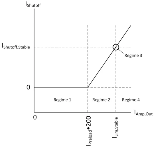
5.4.3
Regimes of Operation
As a whole, the amplifier, when equipped with current limiting systems, can operate in four main regimes, dependent upon the amplifier’s output current, the preload current selected by the end-user, and the transient behavior at its inputs and outputs. The limiting current-output current relationship and regimes are displayed in figure 5.7.
1. Regime 1 is where, before the IP reload mirrored current is overpowered by the mirrored
amplifier output output current, the amplifier functions as normal, with the current limiting circuitry completely shut off, with no current flowing through it.
2. In regime 2, as the amplifier’s output current begins to increase beyond that of 200 · IP reload, then the mirrored output current is transferred into the limiting circuitry.
The limiting circuitry then begins to shut off buffers, clamp buffer outputs into cutoff, disable transmission gates, and interrupt the signal at high-impedance nodes. The current responsible for these behaviors is directly proportional to the amplifier’s output current above the 200·IP reloadvalue. This regime is characterized by decreased amplifier
performance, as the H-bridge portion of the input stage gradually shuts off and the low-power differential pair input begins to dominate the behavior of the amplifier as a whole. Midway through this regime, the H-bridge portion of the amplifier input stage is completely shut off and the system as a whole can be analyzed as a current-limiting system working on a differential pair amplifier.
3. In regime 3, as the output current continues to increase, the limiting current increasing proportionally with it will eventually reach a point where it meets or slightly exceeds the equivalent currents being driven by the differential pair input stage. From here, the current limiting signal chain can be analyzed as a system not unlike that of the LT1970 current limiting system in figure 4.2. This regime is characterized by the inputs of the amplifier being significantly apart (typically at the point where input protection diodes trigger), with the output current sitting at a stable, limited amount. The amplifier stays in this regime until the output current decreases, at which point it returns to the third regime.
4. Regime 4 is never entered in the DC case, and is the situation in which, temporarily, the amplifier can source more than the stable limit current in the third regime. This can occur when the inputs of the amplifier are quickly pulled apart, especially when the amplifier is being used to drive a load with a capacitive component that would look like a zero-impedance short in response to an instantaneous step or rapid signal.
Figure 5.7: Plot of different current-limiting regimes that the amplifier can inhabit
An ideal current-limited amplifier would function uniformly across all current levels below the stable current limit, and the limiting would happen instantaneously when needed. In terms of the regimes discussed, this would equate to an amplifier that could only exist in regimes 1 and 3. In the case of the amplifier discussed, this can be approximated by increasing the slope of the shutoff limiting current in response to the output current in regime 2. However, this response cannot be accentuated past a certain point, as the feedback loop consisting of the amplifier and its current limiting system can become unstable, driving an oscillatory current into the load. In the cases where this shutoff behavior is gained too high, the current increases past the stable shutoff point in regime 3, entering regime 4, then the current limiting circuitry overcorrects, sending the system past regime 2 and back into regime 1, where the
output current begins to increase, skipping over regimes 2 and 3 and back into 4, only to repeat this behavior until the DC situation allows for the amplifier to stay in regime 1.
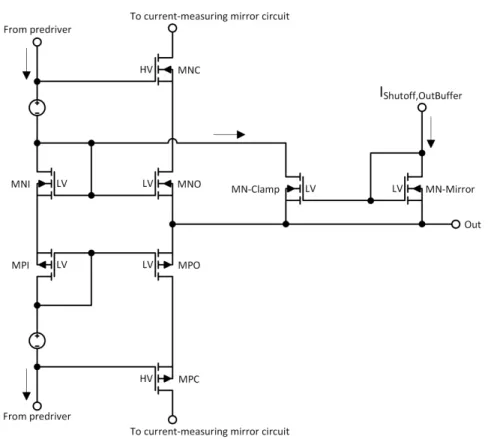
5.4.4
Output Buffer Clamp
The first method by which the current is limited is by clamping the output devices of the output buffer on the amplifier. Figure 5.8 displays the output buffer with source-side current limiting in place. As the amplifier enters and inhabits regime 2, the current IShutof f,OutBuf f er
ramps up, which is mirrored from device MN-Mirror to device MN-Clamp. This has a twofold effect in first redirecting currents, then shutting off certain devices.
Figure 5.8: Output buffer shutoff circuit for source-side current limiting
From the perspective of currents, this current mirroring steals some of the DC source current that is supplied to device MNI through the predriver, routing it through device MN-Clamp’s channel instead, through to the output. This reduction in current through device MNI causes
a reduction in the voltage it generates as a diode-connected device, reducing the total voltage prop-up from the gate of MNO to the gate of MPO, leading to a reduction in the maximum current drive capability of the output buffers.
From the perspective of voltage limiting, as the amplifier gets to the portion of regime 2 that approaches regime 3, MN-Clamp’s channel connection from the gate of device MNO to the output (the source of device MNO) becomes conductive enough such that the output device MNO has its gate tied to the output potential, lowering the VGS of the device sufficiently
such that it enters the cutoff regime and stops conducting current to the output.
5.4.5
Input Buffer Deactivation
To properly limit the current at the output, it is necessary to take the H-bridge portion of the input and remove it from the signal chain. After this is accomplished, then the amplifier acts as a weak differential pair amplifier and current can be limited as a normal amplifier would.
Part of taking the H-bridge portion out of the signal chain is disabling the input buffers for the H-bridge. The first method by which this can be done is through starving the diode-connected devices that serve to prop-up the input of the buffers. Figure 5.9 displays one input buffer with a current source representing the shutoff circuitry. In regime 1, the current source, IShutof f,InBuf f er is disabled, and does not conduct. As the amplifier-limiter system enters
regime 2, IShutof f,InBuf f er ramps up, redirecting some of IBias through it. By redirecting
the IBias current through it, less current goes through low voltage devices MNI and MPI,
reducing the resultant VGS generated across them, decreasing the current drive capability
of devices MNO and MPO. Eventually, IShutof f,InBuf f er becomes large enough such that it
is greater than IBias, and the reverse-bias protection diodes, DN and DP, become forward
VG,M N I− VG,M P I = −2 · VF W D, (5.4)
where VF W D denotes the forward voltage drop of a protection diode. This negative voltage
difference from n-type to p-type devices in the buffer reverse biases the output devices MNO and MPO, driving both of them into the cutoff regime and subsequently stopping any current drive capability they had previously, leaving only the differential pair portion of the input stage to travel through the signal chain and affect the output.
5.4.6
Transmission Gates
In addition to disabling the input buffer by starving it of current, a secondary means by which to disable the H-bridge part of the input stage exists. On figure 5.9, two low voltage n-type devices have their channels connected bidirectionally with each other in series with the source outputs of MNO and MPO, as well as the H-bridge buffer output. These two devices make up the n-type transmission gate that has its control node tied to potential VA.
In regime 2, as IShutof f,InBuf f er increases to and beyond IBias, then diode devices DN and
DP become forward-biased. Through this current and associated drop across DN, VAwill sit
at a potential one diode drop below the input. In the current-starved state , the sources of devices MNO and MPO will join at the pre-switch buffer output and have a potential close to that of the input. As VAwill be below the voltage potential on each side of the transmission
gate, the transmission gate will effectively close, cutting off the H-bridge dynamic current from the signal chain.
For the transmission gates, purely n-type devices were chosen due to variations in the process that give n-type devices higher gm values for conduction, higher ftcharacteristics, and higher
breakdown current densities.
5.4.7
High-Z Gain Node Manipulation
After the H-bridge portion of the input stage has been disabled or cut from the signal chain, it becomes possible to limit current by means of interrupting the amplifier’s signal chain. As the shutoff currents from the limiting circuitry can be thought of in terms of redirecting and amplified currents once regimes 2-4 are entered, using the amplifier’s own high impedance nodes is a convenient way to alter the output.
Figure 5.10: High-Z gain node manipulation for source-side limiting
Figure 5.10 displays the mechanism by which source-side current limiting happens at the high impedance node of the amplifier. Once regime 2 (and regimes 3 and 4) is entered, IShutof f,HighZ begins ramping up. This current is mirrored onto the top-side and bottom-side
high impedance nodes linked together by the Monticelli cell. The positive current being dumped into the high impedance nodes raises the potential of gate nodes on the inverting rail to rail predriver, driving the potential of its output lower, closer to the VSS,HV rail,
low-ering the output from the output buffer, presumably helping to reduce the current output from the buffer into the load.