HAL Id: hal-02332336
https://hal.archives-ouvertes.fr/hal-02332336
Submitted on 29 Jul 2020
HAL is a multi-disciplinary open access
archive for the deposit and dissemination of
sci-entific research documents, whether they are
pub-lished or not. The documents may come from
teaching and research institutions in France or
abroad, or from public or private research centers.
L’archive ouverte pluridisciplinaire HAL, est
destinée au dépôt et à la diffusion de documents
scientifiques de niveau recherche, publiés ou non,
émanant des établissements d’enseignement et de
recherche français ou étrangers, des laboratoires
publics ou privés.
TCAD investigation of zero-cost high voltage transistor
architectures for logic memory circuits
Jordan Locati, Christian Rivero, Julien Delalleau, V. Della Marca, Karine
Coulié, Jordan Innocenti, Olivier Paulet, Arnaud Regnier, Stephan Niel
To cite this version:
Jordan Locati, Christian Rivero, Julien Delalleau, V. Della Marca, Karine Coulié, et al.. TCAD
inves-tigation of zero-cost high voltage transistor architectures for logic memory circuits. 2019 International
Conference on Simulation of Semiconductor Processes and Devices (SISPAD), Sep 2019, Udine, Italy.
pp.1-4, �10.1109/SISPAD.2019.8870384�. �hal-02332336�
978-1-7281-0940-4/19/$31.00 ©2019 IEEE
TCAD investigation of zero-cost high voltage
transistor architectures for logic memory circuits
Jordan Locati, STMicroelectronics 13106 Rousset, France
[email protected] Vincenzo Della Marca Aix-Marseille University CNRS, IM2NP UMR 7334 F-13397 Marseille, France [email protected] Olivier Paulet STMicroelectronics 13106 Rousset, France [email protected] Christian Rivero STMicroelectronics 13106 Rousset, France [email protected] Karine Coulié Aix-Marseille University CNRS, IM2NP UMR 7334 F-13397 Marseille, France [email protected] Arnaud Regnier STMicroelectronics 13106 Rousset, France [email protected] Julien Delalleau STMicroelectronics 13106 Rousset, France [email protected] Jordan Innocenti STMicroelectronics 13106 Rousset, France [email protected] Stephan Niel STMicroelectronics 13106 Rousset, France [email protected]
Abstract— In this paper, a new device architecture has been
studied by TCAD process simulations in order to provide the improvements on the electrical characteristics. We focus mainly on the drain-bulk junction breakdown voltage, of a double 130 nm poly gate transistor for Non-Volatile Memory technology. It is used as a word line select transistor, handling the drain voltage up to 13 V. The proposed structure has been implemented on silicon and the electrical measurements demonstrate the good predictability given by simulations. Finally, a new zero-cost added process asymmetric architecture is also studied to propose further improvements in terms of footprint or electrical characteristics.
Keywords—MOSFET architecture, junction engineering, junction breakdown
I. INTRODUCTION
Nowadays, as the memory density is increasing, the maintaining of low energy consumption is a major challenge for the logic circuits. The scaling of peripheral components, such as high voltage transistors (HV), remains complicated, even if it is possible to reduce the size of memory point. This is a crucial point for the memory array operation in charge storage technologies. In order to guarantee a good product functionality, the HV transistors must assure a drain-bulk junction breakdown voltage (BV) greater than 13 V with a low leakage current. The “more than Moore” [1] approach leads, in the case of HV transistors to a drastic drop in break down voltage or a strong increase of static leakage. To prevent these problems, it is necessary to explore new HV architectures. Therefore, in this work, we investigate a new double gate MOS transistor to improve performances without adding extra photolithography operations and then process cost. Two-dimensional simulations are performed using Synopsys® [2] [3] Technology Computer Aided Design (TCAD) simulator to predict and compare the fabrication process and electrical characteristics of proposed device with respect to the conventional one. First, TCAD process and electrical calibration of the standard architecture is needed to be predictive for the development of new architectures. Then, after obtaining promising simulation results on the proposed architecture, it has been manufactured in 130 nm Non-Volatile
Memory (NVM) technology node. The electrical characterizations demonstrate the good predictability given by simulations. Finally, to deeply push the study on TCAD simulations, we propose an asymmetrical HV transistor for scaled technologies.
II. DEVICES ARCHITECTURES
Fig. 1a shows the assembled TCAD/TEM (Transmission Electron Microscopy) view of the conventional 13V double gate nMOS architecture having a self-aligned (SA) gate length in a range of 0.6-0.9 μm. As the fabrication is integrated in a charge storage memory process flow, it is free to obtain a select transistor with a double-gate. The first poly1 layer, result from the floating gate deposition step, and the second layer (poly2) is a consequence of a control gate fabrication. These are shorted to obtain a single gate terminal. Both polysilicon gates are etched by a single operation called Self Aligned Etch (SAE). TCAD simulation in the Fig. 1b shows that the leakage current, when a 13 V drain voltage is applied, mainly comes from the drain-bulk junction under the gate overlap region. This is due to the doping junction profile. The aim of our study is to propose a new architecture that solves this weakness by varying the length of the poly2 layer with respect to the poly1.
In Fig. 2a a well-known architecture of drift-MOS [4] is also represented. It enables to reach a better BV. The electric field across the drain-bulk junction can be mitigated using low doped implants [5]. Moreover, the increase of the distance between the drain contact and the junction allows to obtain a
Fig. 1. Cross-section of the conventionnal double gate nMOS a) Two-dimensional Sprocess simulation and Transmission Electron Microscopy (TEM) are assembled. b) Leakage current observed during a high voltage biasing (13 V) on drain terminal using Sdevice simulation. The source, gate and bulk are grounded.
Fig. 2. Cross-section of double gate architecture: a) drift-nMOS and b) nMOS-T assembled with a Transmission Electron Microscopy (TEM) picture.
high drain resistance and thus to enhance the breakdown voltage limit [6]. After the poly1 gate etching, three consecutives boron implantation are made in order to control the punch-through current leakage [7] and the threshold voltage (Vth). Then, a phosphorus lightly doped drain (LDD) implantation is made to create source and drain regions. Oxide-nitride-oxide stack (ONO) is processed for the NVM and the second polysilicon layer is thus deposited by Low Pressure Chemical Vapor Deposition (LPCVD) at 620 °C, and etched with an overflow on both sides, followed by a heavily N+ arsenic implantation close to the surface to finally obtain the source and drain regions. The main drawback of this architecture is the footprint. The transistor length increased by 40% compared to the conventional architecture.
A new architecture studied in this paper is proposed in Fig. 2b[8]. We called it “MOS-T” [8]. The TEM picture is assembled with the TCAD sketch. This device configuration allows to use a portion of poly1 gate to implant the LDD regions saving the transistor size. Contrary to the SA architecture, the double-gate is etched by two different steps. First, the poly1 is immediately etched after the deposition. Then, the poly2 is etched after deposition shorter to an identical dimension on both sides than the poly1 gate. In this case, the drain-bulk junction under the gate overlap region has a smoothed profile to achieve an increased junction BV [9]. Fig. 3a shows the main standard process operations to develop the SA architecture. The LDD source/drain implantations are made after the SAE operation and before the poly2 etch (not used for the SA transistor). However, for the MOS-T transistor, the LDD implantations must be shifted after the poly2 etching (Fig. 3b). This is mandatory to obtain the source and drain regions, because of the higher thickness of poly2 that is two times ticker than the poly1. The shift of these operations does not impact the functioning of the other components because they are specific to the SA transistor.
Fig. 3. Main process operations of (a) Standard SA architecture (b) MOS-T architecture.
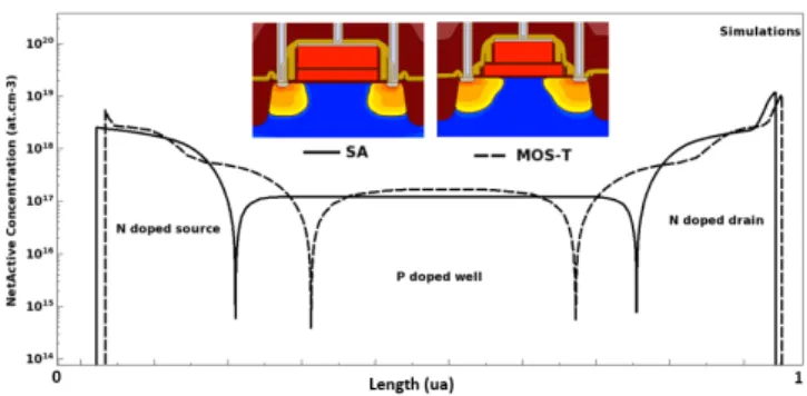
Fig. 4. Simulated NetActive Concentration in channel device versus channel length for conventional SA and MOS-T transistors.
The conventional SA and the MOS-T architectures use an identical well (EPM13V) and source/drain implants. For these last, the phosphorus implantations are made in two steps in order to achieve a smooth junction profile. In Fig. 4, the simulation of the effective channel length (Leff) for the
MOS-T and SA transistors is plotted. Because of the LDD implantations through the polysilicon gate, we can observe a Leff reduction of 35 %, for the MOS-T. This impacts the
threshold voltage with a decrease of 200 mV. Thanks to TCAD simulations, the dose of the lowest boron energy implantation localized in the channel region has been increased by 40 % with respect to the SA transistor. The implantation energy was also investigated through TCAD without significant improvements. Changing the order of the process steps and avoiding extra lithography operations, the fabrication cost is thus saved.
III. SA AND MOS-T COMPARISON
A. Electrical calibration for TCAD prediction
In order to evaluate the performances of the new architecture, the simulations were optimized on the already existing SA transistor to be predictive for the proposed one. In preamble, the device morphologic calibration such as gate oxide thickness or poly gate doping, was done before the MOS architecture investigation. For example, the boron segregation parameter [10] has been modified from 3·1018 cm-3 to 5·1017
cm-3 to adjust the boron concentration near to the silicon oxide
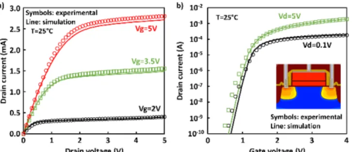
interface. Poisson and drift diffusion models are used for the simulation of carrier transport associated to an avalanche model to simulate the junction comportment at high drain voltages. We are thus able to fit experimental measurements to be predictive in the simulation of the MOS-T. Higher width gate than the real device dimensions has been used for the calibration to avoid narrow channel effect [11]. The Fig. 5a and Fig. 5b show the simulated and measured electrical characteristics of drain current (Id) versus drain (Vd) and gate (Vg) voltage (Fig. 5a and Fig. 5b respectively). In 2D simulations, the back end of line (BEOL) is not considered. A 1.3 kΩ source/drain access resistance has been used in order to be realistic in the ON state operation (Vg>Vth).
Fig. 5. Simulated and measured electrical characteristics of conventional transistor. a) Drain current versus drain voltage for different gate biasing. b) Drain current versus gate voltage for different drain bias conditions.
The MOS-T simulations have been carried out using the same models implemented for the SA transistor. The drain current as a function of the drain voltage characteristics were simulated to qualitatively verify the improvement on BV parameter. The comparison between the conventional SA and MOS-T architectures is shown in Fig. 6, no significant variation of leakage current is observed while an improvement of the BV up to 1.5 V is reached. Even if the Leff of MOST transistor is decreased, the leackage current is
limited by the triple Boron channel implantation and a double LDD step. The achieving of a smoother drain/bulk juction enables an electric field decreasing with a consequent BV increasing. This, together with the maintaining of the footprint, makes the MOS-T architecture suitable for the non-volatile memory logic circuit design.
B. Electrical characterization
Based on the good results obtained by TCAD simulations, MOS-T has been manufactured on 200 mm wafers.
The Fig. 7 shows the experimental Id-Vd characteristics of the SA and MOS-T transistors in a wide range of temperatures in the OFF-state. During these tests the gate, source and bulk terminals were grounded. The simulation prediction was accurate at room temperature. At low and room temperature, the electrical characteristics show two different slopes while the drain voltage is increased. At the beginning, the leakage current starts to increase slowly following the typical impact ionization contribution [12]. While the avalanche contribution becomes dominant for the drain voltage increasing. We can see that for the highest temperature (150 °C) the leakage current is suddenly around 30pA for both devices due to the punch through current, but
Fig. 6. Simulated drain current versus drain voltage for conventional SA and MOS-T architecture.
Fig. 7. Drain current measured of MOS-T and SA transistor as a function of drain voltage for different temperatures.
the MOS-T architecture improves the breakdown voltage up to 2.5 V. Hence, with the same footprint, both leakage current and breakdown voltage constraints have been respected. Concerning the operation in the ON-state, experimental comparison of Id-Vg characteristics is shown in Fig. 8. We can see there is no variation in the threshold voltage as desired and a difference in the conduction current (Vg>Vth) around 5 % between the SA and MOS-T explained by the higher resistance of the source and drain region induced by the LDD implants.
The promising results obtained by simulations have been confirmed by electrical characterizations. Taking advantage of implanting through the poly1 gate allows to gain up to 2.5 V on BV, 1 V more than expected by simulation.
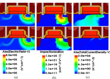
In order to explain this improvement, we took a look at different simulation results such as the electric field, the impact ionization and total current density generated during a 10 V stress applied on the drain. As we can see in Fig. 9a, the electric field is clearly mitigated by the LDD until the P-N junction for the MOS-T while it remains important and concentrated in the junction space charge region for the SA transistor.
This, if the electric field is strong enough, can results in the creation of free electron-hole pairs induced by the impact ionization mechanism (Fig. 9b) for the SA transistor thus inducing quickly the avalanche breakdown. Meanwhile, the electric field across the junction for the MOS-T is weak to improve the avalanche mechanism and it needs higher voltage on the drain. The consequences are shown in Fig. 9c, where the junction leakage current density is plotted. The current induced by the avalanche phenomenon is minimized for the MOS-T.
Fig. 8. Drain current measured of MOS-T and SA transistor as a function of gate voltage for a 0.1 V drain bias applicated.
Fig. 9. Two-dimensional electrical simulation of SA and MOS-T transistor. a) electric field, b) impact ionization and c) total current density generated during 10 V stress applied on drain terminal using Sdevice simulation. The source, gate and bulk are grounded.
IV. ASYMMETRICAL MOS-T
In order to go further in the MOS-T study, we have evaluated the impact to the poly2 gate alignment on the threshold and breakdown voltage. Several simulations were done from the initial poly2 gate position until the case where the poly1 is aligned to the poly2 gate on the source side, in order to extend the LDD implant for the drain region. No additional process steps are required to evaluate this architecture.
The consequences on the BV are shown in the Fig. 10. We can expect an increase up to 1 V taking advantage of asymmetrical architecture. No significant Vth variations have been observed (<60 mV) since there is no variation in the effective length. Furthermore, this option potentially allows to find a tradeoff between the transistor length and the BV to address different applications.
Fig. 10. Simulated drain current as a function of drain voltage for asymmetrical MOS-T.
V. CONCLUSION
This paper presents a new double gate MOS architecture. The simulation results are in agreement with the experimental electrical characterizations, demonstrating the TCAD modeling predictability. With the combination of a source and drain implantation and a shorter control gate, we were able to create LDD regions for free and so to provide with the MOS-T architecture a better breakdown voltage in regards of the SA architecture without additional lithography operations. Finally, we demonstrate that it is possible to implement an asymmetrical gate to extend the LDD region for the drain side increasing the BV allowing to explore footprint reduction.
REFERENCES
[1] Gordon E. Moore, “Cramming more components onto integrated circuits,” Electronics, vol. 38, NO. 8, pp. 114, April 1965
[2] Synopsys®, “Sentaurus Process,” Version N-2017-09-SP1 [3] Synopsys®, “Sentaurus Device,”,Version N-2017-09-SP1
[4] H. Brech et al, ”Record Efficiency and Gain at 2.1GHz of High Power RF Transistors for Cellular and 3G Base Stations,” IEEE International Electron Devices Meeting 2003
[5] R. Marjorie, G. PA, L. Kishore K, “Analysis Breakdown in New Step gate Structures with Graded LDD,” IJCSNS International Journal of Computer Science and Network Security, vol. 17, NO. 4, April 2017 [6] J. Vinson, J. Bernier, G. Croft, J. Liou , “ESD Design and Analysis
Handbook,“ Springer Science & Business Media, December 2012 [7] R. Dennard, F. Gaensslen, H. Yu, V. Rideout, E. Bassous, A. Leblanc,
“Design of ion-implanted MOSFET’s with very small physical dimensions”, Proceeding of EEE, vol. 87, NO. 4, April 1999. [8] C. Rivero, J. Delalleau, “Double-gate MOS transistor with increased
breakdown voltage”, US 2019/0027566 A1, January 2019
[9] Y. Yamaguchi et al, “Source to Drain Breakdown Voltage Improvement in Ultrathin-Film SOI MOSFET’s Using a Gate Overlapped LDD Structure”, IEEE Transactions on Electron Devices, vol. 41, NO. 7, July 1994
[10] C. Machala, R. Wise, D. Mercer, A. Chatterjee, “The Role of Boron Segregation Parameter and Transient Enhanced Diffusion on Reverse Short Channel Effect”, SISPAD’97. 1997 International Conference on Simulation of Semiconductor Processes and Devices
[11] P. Wang, “Device Characteristics of Short-Channel and Narrow-Width MOSFET’s”, IEEE Transactions on Electron Devices, vol. ED-25, NO. 7, July 1978
[12] S.M. Sze, “Physics of Semiconductor Devices”, A. John Wiley & Sons, p. 45, 1981