Publisher’s version / Version de l'éditeur:
Vous avez des questions? Nous pouvons vous aider. Pour communiquer directement avec un auteur, consultez la première page de la revue dans laquelle son article a été publié afin de trouver ses coordonnées. Si vous n’arrivez pas à les repérer, communiquez avec nous à [email protected].
Questions? Contact the NRC Publications Archive team at
[email protected]. If you wish to email the authors directly, please see the first page of the publication for their contact information.
https://publications-cnrc.canada.ca/fra/droits
L’accès à ce site Web et l’utilisation de son contenu sont assujettis aux conditions présentées dans le site LISEZ CES CONDITIONS ATTENTIVEMENT AVANT D’UTILISER CE SITE WEB.
Physical Review. B, Condensed Matter and Materials Physics, 80, 4, p. 41403,
2009
READ THESE TERMS AND CONDITIONS CAREFULLY BEFORE USING THIS WEBSITE.
https://nrc-publications.canada.ca/eng/copyright
NRC Publications Archive Record / Notice des Archives des publications du CNRC :
https://nrc-publications.canada.ca/eng/view/object/?id=b975e415-0e63-4af9-83ed-65f38fd96e58
https://publications-cnrc.canada.ca/fra/voir/objet/?id=b975e415-0e63-4af9-83ed-65f38fd96e58
NRC Publications Archive
Archives des publications du CNRC
This publication could be one of several versions: author’s original, accepted manuscript or the publisher’s version. / La version de cette publication peut être l’une des suivantes : la version prépublication de l’auteur, la version acceptée du manuscrit ou la version de l’éditeur.
For the publisher’s version, please access the DOI link below./ Pour consulter la version de l’éditeur, utilisez le lien DOI ci-dessous.
https://doi.org/10.1103/PhysRevB.80.041403
Access and use of this website and the material on it are subject to the Terms and Conditions set forth at
Surface-directed spinodal decomposition in hafnium silicate thin films
Surface-directed spinodal decomposition in hafnium silicate thin films
J. Liu,1X. Wu,2W. N. Lennard,1and D. Landheer2
1Department of Physics and Astronomy, University of Western Ontario, London, Ontario, Canada N6A 3K7 2Institute for Microstructural Sciences, National Research Council of Canada, Ottawa, Ontario, Canada K1A 0R6
共Received 13 April 2009; revised manuscript received 9 June 2009; published 16 July 2009兲
Hf distributions in as-grown and annealed 共HfO2兲0.25共SiO2兲0.75films with thicknesses in the range of 4–19
nm were investigated by high-resolution transmission electron microscopy, high angle annular dark field scanning transmission electron microscopy and angle-resolved x-ray photoelectron spectroscopy. Composition waves normal to the film surface were observed providing evidence for surface-directed spinodal decomposi-tion in the pseudobinary 共HfO2兲x共SiO2兲1−xalloy system.
DOI:10.1103/PhysRevB.80.041403 PACS number共s兲: 68.37.Og, 64.75.St, 05.70.Fh
Spinodal decomposition 共SD兲 is a diffusional phase sepa-ration whereby a local composition fluctuation reduces the overall free energy of the system.1 In the bulk of a binary mixture experiencing SD, a description of the composition in the solution will be a superposition of sine waves of fixed wavelength, but random in orientation, phase, and amplitude in the initial stage where the linear theory is applicable.2The average size of the single-phase domains then grows with time corresponding to a coarsening of the structure.3 Re-cently, it has been recognized that for thin-film geometry, SD may interact with wetting phenomena resulting in a very different structure at the surfaces compared to the bulk behavior.4–7 This phenomenon has been called surface-directed spinodal decomposition 共SDSD兲. SDSD simulations show that a composition wave perpendicular to the surface forms at the surface due to the preferential attraction of the surface to one of the two components.6 This wave then propagates into the bulk of the film and decays because of thermal noise. Most experimental studies in SDSD have been carried out in polymer mixtures where a small self-diffusion coefficient slows the SD dynamics and the associated phase diagrams can be tailored.4,5 While it is predicted that SD could occur generally in any two-component system whose phase diagram shows a miscibility gap, such as ZrO2-SiO2, HfO2-SiO2, La2O3-SiO2, Y2O3-SiO2,8 and Al2O3-SiO2, ex-perimental observations of SDSD in thin solid films have never been reported.
As complementary metal oxide semiconductor 共CMOS兲 technology progresses, scaling of the traditional gate dielec-trics, i.e., SiO2 and SiOxNy, enters the nanometer regime.9
In this thickness range, the increase in direct tunneling current through the gate oxide raises power consumption and device reliability issues. Numerous efforts have been carried out to search for materials 共so called high 兲 with
dielectric constants larger than SiO2 so that a thick gate in-sulator layer could be used to reduce the leakage current while improving transistor performance.10 Pseudobinary al-loys 共ZrO2兲x共SiO2兲1−x and especially 共HfO2兲x共SiO2兲1−x are of great interest as replacement high- dielectric materials
for SiO2 and SiOxNy in CMOS technology.11 Amorphous
thin films are suitable for CMOS transistors since grain boundaries in polycrystalline structures can become con-ducting paths.12 However, phase separation has been re-ported in 共ZrO2兲x共SiO2兲1−x and 共HfO2兲x共SiO2兲1−x systems
with x = 0.15– 0.80 at a typical dopant activation temperature with the attendant crystallization of ZrO2 or HfO2.13,14 Kim and McIntyre8 calculated the metastable extensions of the miscibility gap and spinodal for the ZrO2-SiO2system based on available phase diagrams and predicted that, upon rapid thermal annealing at conventional device processing tem-peratures, the 共ZrO2兲x共SiO2兲1−x system with composition in the spinodal 共x = 0.1– 0.6兲 will phase separate into two phases having compositions given by the metastable extensions of the miscibility gap. They further simulated the effect of the 共ZrO2兲x共SiO2兲1−x film/Si substrate interface on SD and pre-dicted a composition wave normal to the substrate surface, which decays when propagating into the bulk of the film. It is expected that the 共HfO2兲x共SiO2兲1−x system would experi-ence the same kind of phase separation during annealing due to the similarity of the chemical properties of the Hf and Zr silicates. However, such a SDSD in oxide systems has never been observed experimentally. In this Rapid Communication, we report the first observation of SDSD in thin solid films, i.e., 共HfO2兲x共SiO2兲1−x films, with x ⬇ 0.25, which is in the predicted spinodal range of the Zr共Hf兲O2-SiO2system.
Thin films with composition 共HfO2兲0.25共SiO2兲0.75 were grown on p-type Si 共100兲 substrates by atomic layer deposition 共ALD兲 using the precursors tetrakis共diethylami-do兲hafnium and tris共2-methyl-2-butoxy兲silanol. The detailed growth procedure has been described previously.15ALD uti-lizes the self-limiting reaction mechanism between gaseous precursors and the surface species to produce a thin-film one atomic layer at a time.16During a growth cycle, each precur-sor was introduced separately into the deposition chamber. Alternate precursor pulses were separated by an inert gas purge step. The precursor pulse cycles were repeated until the desired film thickness was achieved. Prior to deposition, the substrate was heated to 500 ° C for 300 s in O2 environ-ment to oxidize the H-terminated surface. In situ x-ray pho-toelectron spectroscopy 共XPS兲 data showed that the oxida-tion process resulted in a ⬍0.5 nm Si thermal oxide. Films with thickness in the range of 4–19 nm were grown while the substrates were held at 350 ° C. In order to investigate the Hf depth profiles in both the as-grown and annealed films, 具011典 cross-sectional transmission electron microscope 共TEM兲 samples were prepared using standard dimpling and ion mill-ing procedures and characterized by high-resolution trans-mission electron microscopy 共HRTEM兲 and high angle
an-nular dark field scanning transmission electron microscopy 共HAADF-STEM兲 in a JEOL JEM-2100F TEM operating at 200 kV. The HRTEM and HAADF-STEM images are re-ferred to as bright field 共BF兲 and dark field 共DF兲 images, respectively. Film compositions near the surface were also investigated by angle-resolved XPS 共ARXPS兲 using mono-chromatic Al K␣ x rays. An ex situ rapid thermal anneal
共RTA兲 was subsequently performed in N2at 800 ° C for 6 s. Figures1共a兲and1共b兲show the BF and DF images of a 5 nm as-grown film. In Fig.1共a兲, the darker area near the sur-face indicates a region of higher Hf concentration relative to the brighter area close to the substrate. The contrast in Fig. 1共b兲is reversed relative to Fig.1共a兲such that the DF image is more sensitive to the atomic number of the constituent atoms. Both images confirm the Hf-rich top region and the Hf-deficient 共i.e., Si-rich兲 bottom region of the film. Addi-tional TEM images of thinner 共⬃4 nm兲 as-grown films show a similar structure. Figures 1共c兲 and1共d兲 show the DF im-ages of 6.4 and 12 nm films, respectively. In both films, there are Hf-deficient layers at the substrate interface of thickness 0.6 and 1 nm, respectively. These data show that during the film deposition process when the film thickness increases from 5 to ⬎6 nm, some Hf atoms in the Hf-rich layer ap-parent in Fig.1共b兲diffuse toward the substrate. It is difficult to determine whether the entire Hf-deficient layer adjacent to the substrate 关see Fig.1共c兲兴 is thermal SiO2 formed initially during the substrate oxidation process. The Hf-deficient layer in Fig. 1共b兲is not all thermal SiO2 since its thickness is too large, i.e., significantly ⬎0.5 nm, and it is therefore a Si-rich layer of the film.
Figure 2共a兲shows the BF image of the 5 nm film 关Figs. 1共a兲 and1共b兲兴 after RTA. Figures2共b兲 and2共d兲 are the DF images of the films shown in Figs. 1共c兲 and 1共d兲, respec-tively, after RTA. The thickness of all films decreases slightly due to densification during annealing. The Hf profile for the 5 nm film is little changed following RTA: the film separates into two layers with the layer closer to the substrate still Si rich. The 6.4 nm film separates into three layers: a Si-rich layer sandwiched between two Hf-rich layers. The 0.5 nm interface layer in Fig.2共b兲is Si thermal oxide formed during the substrate oxidation process. An 8 nm film after RTA 关Fig. 2共c兲兴 consists of four layers starting from the bottom 共i.e., substrate兲: Si-rich, Hf-rich, Si-rich, and Hf-rich. Figure 2共d兲 shows a very thin ⬃1 nm Si-rich layer on the substrate with
a ⬃2 nm Hf-rich layer on top similar to Fig. 1共d兲. Above these two layers, Hf-rich clusters are mixed with Si-rich clus-ters.
The layered structure shown in the above TEM images provides evidence that SDSD occurs in 共HfO2兲0.25共SiO2兲0.75 films. A composition wave normal to the substrate surface is observed in post-RTA films thinner than 8 nm. If the compo-sition wavelength, C, is defined as the distance between the
centers of the two successive Hf-rich layers, then C
mea-sured from TEM images 关Figs. 2共b兲and2共c兲兴 is ⬃4 nm. If the film is thinner than 8 nm 共i.e., 2C兲, a layered structure is
observed via TEM throughout the entire film: the surface layer is Hf rich and the layer closest to the interface Si oxide can be Si rich or Hf rich depending on the film thickness. If the film thickness is Cor 2C, the layer closest to the
inter-face is Si rich. If the film thickness is 1.5C, the layer closest
to the interface is Hf rich—a surprising result. The film phase closest to the interface was expected to be Si rich since the 共HfO2兲0.25共SiO2兲0.75 films were grown on a very thin Si thermal oxide and the Si-rich phase in the films should have a lower interface energy with this oxide layer. As the film thickens to ⬎2C, a Si-rich layer followed by a Hf-rich layer
is observed at the film/Si interface and there is no continuous Hf-rich layer in the center of the film, indicating a tendency for decay of the composition wave.
Figure 3 shows the BF and DF images of a 19 nm as-grown film where HfO2 crystallites with dimension of 5–8 nm are seen in Fig. 3共a兲. This observation implies that the nucleation and growth of crystalline HfO2have followed SD during the film deposition process. The DF image 关Fig.3共b兲兴 shows that in the 19 nm film, a Si-rich layer is formed on the substrate with a Hf-rich layer above; on top of these two
FIG. 1. 共a兲 BF and 共b兲 DF image of a 5 nm as-grown film. DF images of 共c兲 6.4 and 共d兲 12 nm as-grown films.
FIG. 2. 共a兲 BF image of film shown in Fig.1共a兲after RTA; 共b兲 DF image of film shown in Fig.1共c兲after RTA; 共c兲 BF image of an 8 nm film after RTA; and 共d兲 DF image of film shown in Fig.1共d兲
after RTA.
FIG. 3. 共a兲 BF and 共b兲 DF images of a 19 nm as-grown film. Crystalline HfO2regions are encircled.
LIU et al. PHYSICAL REVIEW B 80, 041403共R兲 共2009兲
layers, Hf-rich and Si-rich clusters are randomly mixed. This image is similar to the simulation results6 for the cross-sectional images of a film experiencing SDSD.
To further study the effect of film thickness on film struc-ture, dilute HF 共0.4%兲 was used to etch back the 6.4 and 12 nm films. Before etching, the 共HfO2兲0.25共SiO2兲0.75films were subjected to the usual RTA process to reduce the etching rate17and to achieve the layered structure shown in Fig.2共b兲 for the 6.4 nm film. After etching, the RTA step was re-peated. Spectroscopic ellipsometry was used to monitor the etching rate, 共i.e., the film thickness was measured after ev-ery 4 s etch兲. For 6.4 nm film, XPS was also used to measure film thickness18 before and after etching. Figure 4共a兲shows the BF image of the 6.4 nm film after RTA, HF etch, and RTA. A 2 nm layer of the film was removed after HF etching; i.e., the top Hf-rich layer in Fig. 2共b兲 was removed. The Hf-rich layer closest to the substrate in Fig.2共b兲has diffused to the top of the film after the HF etch and following the second RTA, resulting in a structure similar to that in Fig. 2共a兲, which corresponds to a 5 nm film 共annealed兲 on a Si substrate. The thickness of the film shown in Fig. 4共a兲is 1 nm greater than expected after HF etching and RTA, which can likely be explained by oxidation of the Si substrate dur-ing the annealdur-ing process via water molecules absorbed in the film during the HF etching process. Figure 4共b兲 shows the BF image of the 12 nm film 关Fig. 1共d兲兴 after RTA, HF etch 共removing ⬃6 nm兲, and RTA. The Si-rich layer closest to the substrate is thermal SiO2formed after HF etching and the second RTA. The predominantly layered structure, which was not observed for the 12 nm film 关see Fig.2共d兲兴, appears when the film thickness is reduced to a value in the region ⱗ2C.
In SDSD, Cwill increase as the annealing time increases
corresponding to a coarsening of the phase separated structures.6,8 In order to search for this phenomenon in Hf silicate films, longer time anneals were performed for the 6.4 and 12 nm films. Figures5共a兲and5共b兲show the DF and BF images of the 6.4 and 12 nm films, respectively, after a 600 s anneal in N2at 800 ° C. Figure5共a兲shows only one Hf-rich
layer indicating a growth of single phase domain during longer time anneal. The thickness of this film has increased by ⬃2 nm compared to the thickness after RTA 关Fig. 2共b兲兴 as a result of diffusion of the O2impurity in N2to the inter-face where oxidation of the substrate occurs.19 From Fig.
5共b兲, a ⬃3-nm-thick layer of thermal SiO2has grown during the 600 s anneal. HfO2crystallites were observed in this film, again indicating that nucleation and growth occurred after SD during the annealing process. The DF image of this film was similar to Fig. 2共d兲. HfO2 crystallites are not observed for films thinner than 12 nm even after anneal at 800 ° C in N2for 600 s, which is not surprising since the onset of crys-tallization of HfO2 in Hf silicate films depends on film composition20 and thickness.21In the nucleation and growth mechanism, for a nucleus to be stable to further growth, it must reach a critical size. Smaller nuclei are unstable and may dissolve because of surface energy effects and their large surface to volume ratio. Therefore the nucleation and growth process is suppressed in thinner films and a higher temperature is needed for crystallization to occur.21
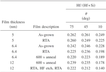
It is difficult to resolve the layer closest to the 共top兲 film surface from the glue that is used to prepare the TEM sample if that layer is Si rich. In order to examine the composition of this surface layer, ARXPS measurements were carried out and the results are presented in TableIfor various photoelec-tron takeoff angles, . The Hf concentration, which is
pro-portional to the Hf/ 共Hf+ Si兲 ratio, decreases toward the sur-face for all films 共which therefore implies an increase in the Si concentration兲. Comparing the Hf concentration in the as-grown and annealed films at= 10°, more SiO2is observed
to diffuse to the film surface during annealing, which sug-gests a wetting of the film surface by the SiO2-rich compo-nent. Previously, simulation results showed that the Si-rich phase contains ⬎98 mol % SiO2 in the 共ZrO2兲x共SiO2兲1−x system after phase separation during 900 ° C anneals.8 As-suming that the Si-rich phase in the 共HfO2兲0.25共SiO2兲0.75films is pure SiO2, then the thickness of the surface layer of the films can be estimated. The escape depth 共e兲 of Si 2p
pho-toelectrons excited by Al K␣x rays in SiO2is 3 nm,18which should be a reasonable estimate for Hf silicate films. The sampling depth then varies from 9 nm 共3e兲 at= 90° to 1.6 FIG. 4. BF images of 共a兲 6.4 and 共b兲 12 nm films after RTA, HF
etch, and RTA.
FIG. 5. 共a兲 DF image of 6.4 nm and 共b兲 BF image of 12 nm films, after 600 s anneal. Crystalline HfO2regions are encircled.
TABLE I. Hf concentration extracted from ARXPS. is the photoelectron takeoff angle.
Film thickness 共nm兲 Film description Hf/ 共Hf+ Si兲 共deg兲 75 45 10 5 As-grown 0.262 0.261 0.249 5 RTA 0.260 0.249 0.225 6.4 As-grown 0.242 0.246 0.228 6.4 RTA 0.225 0.236 0.198 6.4 600 s anneal 0.220 0.223 0.189 12 600 s anneal 0.239 0.235 0.178
nm at = 10°. Assuming that the film composition
deter-mined at = 75° corresponds to the average composition,
then the thickness of the surface SiO2layer is estimated to be ⬃0.4– 0.7 nm, i.e., equivalent to one to two layers of SiO2. The composition of the Hf-rich layer in the films shown in Fig.1共b兲or Fig.2共b兲can also be estimated from the relative thicknesses of the bright and dark layers. For example, the Hf-rich top and bottom layers evident in Fig. 2共b兲 have a composition Hf/ 共Hf+ Si兲 ⬇ 0.32. This value is much lower than the calculated composition 共Zr/ 共Zr+ Si兲 = 0.80兲 共Ref.8兲 of the Zr-rich phase in the ZrO2-SiO2 system which experi-ences SD in this temperature range.
Using grazing-incidence small angle x-ray scattering 共GISAXS兲, Stemmer et al.14 observed interference peaks in the horizontal cuts of their two-dimensional GISAXS inten-sity distribution, which correspond to a Hf concentration fluctuation in the plane of the film with Cvalues of 5 nm in
the 4 nm 共HfO2兲x共SiO2兲1−x films 共x = 0.4兲 after 1000 ° C an-nealing. The observation was confirmed by their plan-view TEM image, which shows interconnected Hf-rich and Si-rich regions. However, these authors did not try to interpret ver-tical cuts of their GISAXS data but still concluded that their observations were inconsistent with SDSD. In contrast, the TEM images reported here always show a layered structure for post-annealed films of thickness ⬍8 nm, which is con-sistent with SDSD.
The diffusion coefficient of Hf in these 共HfO2兲0.25共SiO2兲0.75 films can be estimated from our experi-mental observations. Based on the TEM images shown in Figs. 1共c兲 and2共b兲, the diffusion length of Hf atoms after RTA should be ⱖ1 nm, which suggests a diffusion coeffi-cient for Hf atoms in Hf silicate ⱖ10−19 m2/s at 800 ° C.
In summary, the observation of SDSD in thin solid films is presented. While the configurations in as-grown and an-nealed 共HfO2兲0.25共SiO2兲0.75 films are qualitatively in
agree-ment with the theory of SDSD, i.e., the composition waves normal to the film surface were observed, the observation that the composition of the film layer in contact with the substrate can be affected by film thickness has never been predicted by any SDSD simulation. Presumably, theoretical studies of SDSD could be modified to accommodate these experimental results. At this time, it is difficult to study SDSD in 共HfO2兲0.25共SiO2兲0.75films to determine whether the composition wave obeys the growth law C⬃ t1/3 共Ref. 5兲
because: 共i兲 TEM is a qualitative technique concerning atomic composition; 共ii兲 SD in oxide systems is not easily controlled since the process occurs during the film deposition process; 共iii兲 an alternative kinetic process, viz., nucleation and growth, can impede SD during the late stages of phase separation; and 共iv兲 any O2 impurity in the annealing N2 ambient may also diffuse through the film and oxidize the substrate. While SDSD in the 共HfO2兲0.25共SiO2兲0.75thin films has been confirmed, the composition range for which 共HfO2兲x共SiO2兲1−xfilms experience SD and the resultant com-positions of the phase-separated domains are still open ques-tions.
The present observation of SDSD in 共HfO2兲x共SiO2兲1−x films may present significant device performance and reliability challenges for high- gate dielectric
applica-tions of pseudobinary alloy systems including ZrO2-SiO2, Y2O3-SiO2, La2O3-SiO2,8 etc., and have effects on thin film applications of any two-component system whose phase dia-gram shows a miscibility gap. The ALD growth mechanism for two-component films could also be influenced by SDSD if the film surface is preferentially attracted to one of the two components.
The authors are grateful for the technical assistance of L. Lebrun, G. Parent, and S. Moisa at NRCC and J. Hendriks at UWO. Financial assistance to W.N.L. was provided by NSERC 共Canada兲.
1J. W. Cahn, Trans. Metall. Soc. AIME 242, 166 共1968兲. 2J. W. Cahn, J. Chem. Phys. 42, 93 共1965兲.
3F. S. Bates and P. Wiltzius, J. Chem. Phys. 91, 3258 共1989兲. 4R. A. L. Jones, L. J. Norton, E. J. Kramer, F. S. Bates, and P.
Wiltzius, Phys. Rev. Lett. 66, 1326 共1991兲.
5G. Krausch, C.-A. Dai, E. J. Kramer, and F. S. Bates, Phys. Rev.
Lett. 71, 3669 共1993兲.
6S. Puri and K. Binder, Phys. Rev. E 49, 5359 共1994兲.
7S. K. Das, S. Puri, J. Horbach, and K. Binder, Phys. Rev. E 72,
061603 共2005兲.
8H. Kim and P. C. McIntyre, J. Appl. Phys. 92, 5094 共2002兲. 9P. A. Packan, Science 285, 2079 共1999兲.
10J. Robertson, Rep. Prog. Phys. 69, 327 共2006兲.
11G. D. Wilk, R. M. Wallace, and J. M. Anthony, J. Appl. Phys.
87, 484 共2000兲.
12M. A. Quevedo-Lopez, M. R. Visokay, J. J. Chambers, M. J.
Bevan, A. LiFatou, L. Colombo, M. J. Kim, B. E. Gnade, and R. M. Wallace, J. Appl. Phys. 97, 043508 共2005兲.
13D. A. Neumayer and E. Cartier, J. Appl. Phys. 90, 1801 共2001兲.
14S. Stemmer, Y. Li, B. Foran, P. S. Lysaght, S. K. Streiffer, P.
Fuoss, and S. Seifert, Appl. Phys. Lett. 83, 3141 共2003兲.
15J. Liu, W. N. Lennard, L. V. Goncharova, D. Landheer, X. Wu,
S. A. Ruchworth, and A. C. Jones, J. Electrochem. Soc. 156, G89 共2009兲.
16T. Suntola, Mater. Sci. Rep. 4, 261 共1989兲.
17J. Chen, W. J. Yoo, and D. S. H. Chan, J. Electrochem. Soc. 153,
G483 共2006兲.
18Z. H. Lu, J. P. McCaffrey, B. Brar, G. D. Wilk, R. M. Wallace, L.
C. Feldman, and S. P. Tay, Appl. Phys. Lett. 71, 2764 共1997兲.
19J.-P. Maria, D. Wicaksana, A. I. Kingon, B. Busch, H. Schulte,
E. Garfunkel, and T. Gustafsson, J. Appl. Phys. 90, 3476 共2001兲.
20S. Stemmer, Z. Chen, C. G. Levi, P. S. Lysaght, B. Foran, J. A.
Gisby, and J. R. Taylor, Jpn. J. Appl. Phys., Part 1 42, 3593 共2003兲.
21G. Pant, A. Gnade, M. J. Kim, R. M. Wallace, B. E. Gnade, M.
A. Quevedo-Lopez, and P. D. Kirsch, Appl. Phys. Lett. 88, 032901 共2006兲.
LIU et al. PHYSICAL REVIEW B 80, 041403共R兲 共2009兲