HAL Id: hal-02007142
https://hal.univ-brest.fr/hal-02007142
Submitted on 5 Feb 2019
HAL is a multi-disciplinary open access
archive for the deposit and dissemination of
sci-entific research documents, whether they are
pub-lished or not. The documents may come from
teaching and research institutions in France or
abroad, or from public or private research centers.
L’archive ouverte pluridisciplinaire HAL, est
destinée au dépôt et à la diffusion de documents
scientifiques de niveau recherche, publiés ou non,
émanant des établissements d’enseignement et de
recherche français ou étrangers, des laboratoires
publics ou privés.
Fused deposition modeling : A new technology for the
fabrication
Younès Arbaoui, R Gingat, A Pen, P. Agaciak, D Palessonga, P Roquefort, A.
Maalouf, A. Chevalier, J. Ville, T. Aubry, et al.
To cite this version:
Younès Arbaoui, R Gingat, A Pen, P. Agaciak, D Palessonga, et al.. Fused deposition modeling : A
new technology for the fabrication. International Symposium Space Passive Components Days, Oct
2018, Noordwijk, Netherlands. �hal-02007142�
FUSED DEPOSITION MODELING: A NEW TECHNOLOGY FOR THE FABRICATION
OF MICROWAVE LOADS
Y. Arbaoui(1), R. Gingat(1), A. Pen(1), P. Agaciak(2), D. Palessonga(1), P. Roquefort(2), A. Maalouf(1), A. Chevalier(1), J. Ville(2), T. Aubry(2), P. Queffelec(1) and V. Laur(1)
(1)Lab-STICC, University of Brest, Brest, France
Email: [email protected]
(2)IRDL, University of Brest, Brest, France
INTRODUCTION
Microwave load (or termination) is a one port device which makes it possible to convert efficiently microwave energy into heat. Important parameters of a load are its Voltage Standing Wave Ratio (VSWR) and its power handling capability.
In a receiver, loads are placed at unconnected ports of hybrid couplers or power dividers to keep the VSWR of the signal path as low as possible. They are also commonly used to convert circulators in isolators by ensuring a good isolation between ports.
Coaxial and rectangular waveguide loads are commonly fabricated by using absorbing materials. Materials are chosen depending on the desired power handling capability. Low and medium power rectangular waveguide loads usually consist of lossy composites that are molded or machined in the form of a tongue, multiple steps, tapered spears or a pyramid in order to minimize VSWR over a wide bandwidth.
Molding or machining processes have a high impact on the cost of the termination. In this context, the use of 3D printing technologies appears to be a way to optimize these devices cost, especially during the prototyping step or for the production in small series. Our studies were focused on the use of Fused Deposition Modeling (FDM) which is the cheapest 3D printing method and for which a large number of composite materials that can exhibit interesting absorption properties (high loss tangent) are available.
In this paper, we will at first describe the 3D printing process and materials that were used to fabricate microwave loads. Then, demonstrators in different frequency bands will be described.
MATERIALS AND TECHOLOGIES
The use of additive technologies is a fast, low-cost and easy way to fabricate demonstrators. In recent years, FDM technique, which consists in depositing a fused polymer layer-by-layer to fabricate a 3D object, has been used to realize microwave devices such as antennas [1], filters [2] or transmission lines [3]-[4].
In the absorption domain, dielectric or magnetic losses are required and pure polymer cannot thus be used alone. Several printable composites are now available and their electromagnetic (EM) properties can be compatible with this application. For example, metamaterial absorbers were developed by using metal-filled polymer [5].
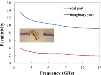
In this study, we used a conductive ABS filament, called here ABS-C, from Torwell Technologies Co. This polymer is filled with carbon particles that strongly increase its dielectric losses. At first, we printed ABS-C slabs with a Makerbot Replicator 2X printer. Toroid samples (square cross section), with an inner diameter of 3.04 mm and an outer diameter of 7 mm, were then micro-machined with a LPKF Protomat 103 milling machine for standard coaxial electromagnetic characterization. S-parameters of the APC7 coaxial line filled with these samples were computed thanks to NRW procedure [6] to extract EM properties of the printed filament. Dielectric properties of ABS-C in the 1-15 GHz frequency band are shown in Fig. 1. This printable material is strongly dispersive with a permittivity that lies between 13.6 at 1 GHz and 9.1 at 15 GHz. In this frequency range, dielectric losses are high (0.2 < tanδ < 0.29) and compatible with absorption applications. These properties were integrated in EM software to design rectangular waveguide microwave terminations at X-band (8-12 GHz).
Fig. 1. Dielectric properties of 3D-printed ABS-C between 1 and 15 GHz. Inset: coaxial air-line and toroid samples of ABS-C.
FABRICATION AND CHARACTERIZATION X-band pyramidal loads
In order to validate the concept of 3D printed loads, the first step consisted in designing and fabricating a simple pyramidal absorber that was inserted in a short-ended WR-90 rectangular waveguide (Fig. 2.a). The dimensions of the pyramid are 9.22 mm x 11.23 mm x 69.21 mm. This device was called hybrid 3D printed load.
A full 3D printed load was also designed and manufactured (Fig. 2.b). The device is self-consistent in that it can be directly connected to a WR-90 waveguide. The total length of the device is 93.3 mm. A UBR100 type flange was printed on base whose transverse dimensions are 32.7 mm x 20.3 mm.
Fig. 2. X-band (a) hybrid load and (b) full 3D printed load.
VSWR levels of these devices were measured and compared with a commercial load (HP Termination 00910-600003 from X11644A HP calibration kit) between 8 and 12 GHz (Fig. 3). A Thru-Reflect-Line calibration was performed. This calibration proved to provide the lowest uncertainties (compared to a SOLT calibration).
The hybrid 3D printed termination shows a VSWR lower than 1.075 over the whole X-band. Return losses of the full 3D printed load are significantly better with a VSWR lower than 1.025 between 8 and 12 GHz. One should note that the measured VSWR uncertainty is less than 0.008 over the measured VSWR levels range.
These performances are similar to the one measured on a precision termination coming from a calibration kit and that hybrid and full 3D printed termination performances have not to be compared because of the difference of dimensions between the two devices.
The simulated VSWR level of the full 3D printed termination is also presented in Fig. 3. Measured and simulated VSWR levels are in good agreement between 8.6 and 12 GHz. At low frequencies (f < 8.6 GHz), simulated VSWR
levels are slightly higher than the ones measured. This difference can be due to small defects of the realized full 3D printed termination whose behavior is difficult to predict in the simulation.
Fig. 3. Comparison of measured VSWR levels of a commercial HP termination, a hybrid 3D printed termination and a full 3D printed termination (with uncertainty bounds) and simulated VSWR level of a full 3D printed
termination as a function of frequency.
The power behavior of the full 3D printed load was also investigated. It was proved that this device can handle 11.5 W (maximum power of the test bench) without any degradation. Moreover, the cost of such devices was estimated to be between 10 and 100 times less than a commercial termination [7].
We then studied the possibility to increase the operation frequency of this new technology. Increasing frequency can lead to technological issues related to a decrease of the dimensions of the printed device.
K-band tapered wedge loads
The objective of this second study was to increase the working frequency of 3D printed load. We decided to design and fabricate K-band (18-26.5 GHz) devices. In this frequency band, WR-42 waveguides have small dimensions (a = 10.67 mm and b = 4.32 mm) so that the topology of the load has to be wisely selected. X-band pyramidal loads revealed that pyramid can lead to printing issues. Indeed, when printed along the axis of the pyramid, it appeared to be difficult to ensure a good definition of the tip because fused polymer did not have time to harden, even if printing speed was slow, when printing so small surfaces. Printing pyramids perpendicularly to their axis requires using a support material that leads to rough surfaces.
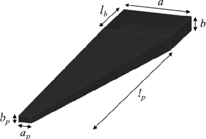
Thus, for this frequency band, we propose another topology called Asymetrical Tapered Wedge (ATW) presented in Fig. 4 [8]. This topology seems to be better suited to 3D printing as the tip of the pyramid, which can be subject to random defects, is placed in a minimum electric field.
Table 1 gives the dimensions of the ATW geometry finally selected, as these gave the best tradeoff between printability and simulated performance. It was demonstrated in [8] that a truncation of the tip do not strongly degrade reflection coefficient of the device. In simulation, these dimensions lead to a S11 parameter of less than -43 dB over the whole
K-band.
Table 1. Dimensions of the ATW geometry (in mm) used to realize microwave terminations
a b lb ap bp lp
10.67 4.32 10 1.2 0.9 40
The load that integrates ATW absorber is shown in Fig. 5. A thickness layer (elay) of 50 µm was used for all the
fabricated ATW absorbers.
Fig. 5. Exploded view of the K-band microwave termination.
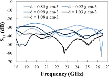
We first studied the effect of the density on the reflection parameter of microwave terminations. As the density of the contour, upper and lower layers and the internal part of the object can be different, we measured the apparent density of each of the ATW geometries by measuring their mass and knowing that the volume of the object is 1.189 cm3. When the internal density (dint) was increased from 50 to 100%, the apparent density increased from 0.85 to 1.08 g.cm
-3
. Fig. 6 shows the reflection level of the microwave termination as a function of frequency for different values of apparent density. The denser geometry (d = 1.08 g.cm-3) makes it possible to obtain a reflection level lower than 34 dB over the whole K-band. Logically, an ATW geometry with an apparent density of 0.85 g.cm-3 should give worse performance. However, in this case return losses remain lower than -27.5 dB between 18 and 26.5 GHz.
Fig. 6. Measured reflection parameter (S11) amplitude as a function of frequency for different apparent densities of
ATW absorbers.
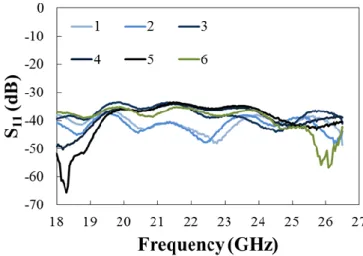
We then studied the reproducibility of the performance of these microwave terminations: six ATW geometries were printed under the same conditions (elay = 50 µm, dint = 100%) and measured. Fig. 7 presents the reflection coefficients of
these microwave terminations as a function of frequency. We observed some noticeable differences of reflection coefficient between the six different 3D-printed ATW loads. However, reflection coefficient is very sensitive to the presence of air gaps between the absorber and the metallic short circuit and it seems that this phenomenon could be mainly due to the manner of insertion of the ATW geometry in the short-circuited waveguide. In the worst case, reflection coefficient remains below -33.5 dB over the whole frequency band. Moreover, as one should recall, no post-machining was performed on the ATW geometries.
Fig. 7. Measured reflection parameter (S11) amplitude as a function of frequency for six different ATW absorbers
printed in the same conditions.
The median value of reflection coefficient is between -36.6 dB and -41.4 dB for these different devices. The small difference in reflection parameter between the terminations supports the reproducibility of this new method of fabrication for microwave terminations.
We thus demonstrated that a wise choice of geometry, that presents a trade-off between microwave performance and printing issues, can lead to reproducible 3D printed microwave loads up to 26.5 GHz without any post-machining. More recently, we interested in printable topologies that can lead to a reduction of the load length.
X-band compact loads
As it was shown previously, 3D printing technique can be used to fabricate pyramidal- or wedge-type loads that present very low reflection levels. However, these topologies are based on a progressive filling of the rectangular waveguide by a lossy dielectric that leads to bulky devices. Thus, we proposed a new concept which was initially based on studies that theoretically demonstrated that excess losses can be achieved by a partial filling of a rectangular waveguide by a lossy dielectric [9]-[10]. In these studies, the propagation constant of Longitudinal Section Magnetic (LSM) modes were investigated in the case of H-plane partially loaded rectangular waveguide. Excess losses can be achieved for a filling factor between 20 to 30% depending on dielectric properties of absorbers.
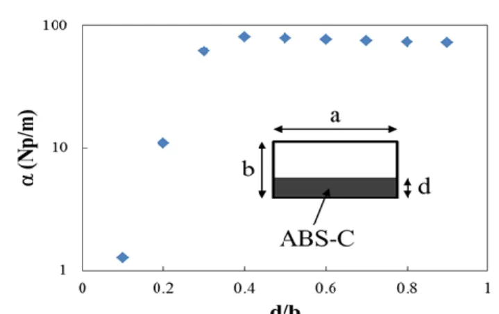
At first, we calculated real part of propagation constant of a H-plane ABS-C partially loaded WR-90 waveguide through EM simulations. Fig. 8 shows attenuation constant α at 10 GHz as a function of filling factor d/b. The evolution is very similar to the one observed in [10] and shows that attenuation constant can be as high as the one of a fully loaded rectangular waveguide for filling factor as low as 30%. Similar trend was observed for E-plane partially loaded rectangular waveguide for Longitudinal Section Electric (LSE) modes.
Fig. 8. Attenuation constant α at 10 GHz as a function of filling factor d/b for a rectangular waveguide partially filled with ABS-C.
Thus, we tried to develop the idea that massive absorption can be achieved with partially transversal loaded regions. However, as a single slab of absorber does not lead to compact microwave terminations, we went further by considering no longer slabs but blocks knowing that such complex structures can be manufactured by FDM technology. In this way, we decided to discretize transversal section of absorber material in order to create blocks of different dimensions. In this case, not only LSE and LSM modes can be excited but also higher order modes leading to a very complex field’s pattern. Such structure can only be optimized though EM simulations. In order to compare this new topology with classical ones (pyramid, wedge…), the concept was applied to the design of a rectangular waveguide termination at X-band (central frequency = 10 GHz, relative X-bandwidth = 15%).
Fig. 9 shows the example of a 4x3 topology for which the length of blocks are denoted l1 to l12. This structure was
called Manhattan-like absorber (MLA) in reference to the famous borough of New-York City. In this example, each block has the same transversal dimensions (5.715 mm x 3.387 mm). The longer block is 19.9-mm long. One should note that, compared to a classical pyramidal absorber, this topology leads to a length reduction of 60%.
Fig. 9. Manhattan-like absorber and terminology chosen for its description.
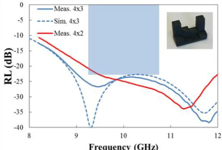
This structure was 3D-printed and measured in a short-ended waveguide from 8 to 12 GHz. Fig. 10 shows simulated and measured return loss as a function of frequency for this 4x3 MLA. This compact termination demonstrates a reflection coefficient that respects specifications and proves a good agreement with simulations.
We also design and fabricate a 4x2 MLA. Simulations show that it is possible to respect specifications with a length 2 times lower than the pyramidal topology (l = 15.4 mm). Measurements do not respect exactly specifications (Fig. 10). However, this 4x2 MLA demonstrates a reflection coefficient lower than -20 dB between 9.17 and 12 GHz.
One should note that we optimized, fabricated and measured different types of MLA (2x1, 2x2, 4x2, 3x4…). The best simulations lead to terminations as short as 7.8 mm in the case of a 2x3 topology. However, experimental validations shows that these very compact terminations are extremely sensitive to dimensional variations and air gaps leading to frequency shifts and reproducibility issues.
Fig. 10. Simulated and measured return loss of a 4x3 MLA and measured one of a 4x2 MLA. Inset: picture of the 3D-printed 4x2 MLA.
CONCLUSION
We investigated the potential FDM technique to realize microwave loads. We demonstrated that low-cost device with high performance can be fabricated by 3D-printing ABS-C composite. As an example, X-band pyramidal loads that have VSWR as low as 1.025 between 8 and 12 GHz were designed, fabricated and measured. This component proves to be stable up to 11.5 W. We also demonstrated that a wise choice of the topology (i.e. trade-off between microwave performance and 3D printing feasibility) can lead to reproducible devices up to 26.5 GHz even without any post-machining. Finally, a new compact topology, compatible with FDM technology, was proposed. We demonstrated that this new topology, called MLA, can lead to a reduction of 50% of the load’s length compared to a classical pyramidal absorber.
FDM technology appears thus to be a way to fabricate low-cost microwave loads. This 3D-printing technique, that makes it possible to realize complex geometries, paves the way to the design of complex microwave loads that allow an improvement of global performance of microwave loads (compactness, reflection coefficient, thermal stability…). However, new printable polymer composites with high temperature stability have to be developed in order to be compatible with space applications. We are currently working on the development of Polyphenylene Sulfide composites, with controlled structure and rheology, that will be soon be used to develop 3D-printed microwave loads with improved thermal stability.
Besides, 3D printing of lossy dielectrics can be applied to other microwave applications such as the fabrication of microwave absorbers for plane-wave attenuation.
ACKNOWLEDGEMENTS
This work was funded by DGA in the framework of ANR ASTRID 3DRAM project.
REFERENCES
[1] J. Castro, E.A. Rojas-Nastrucci, A. Ross, T.M. Weller, J. Wang, “Thermoplastic composites for fused deposition modeling of microwave components,” IEEE Trans. Microw. Theory Tech., vol. 65, no. 6, pp. 2073-2084, June 2017.
[2] C. Tomassoni, R. Bahr, M. Tentzeris, M. Bozzi, L. Perrigrini, “3D printed substrate integrated waveguide filters with locally controlled dieletric permittivity,” in 2016 IEEE Eur.Micr. Conf. Dig., London, UK, Oct. 2016, pp. 253-256.
[3] R. Bahr, L. Perregrini, T. Le, M.M. Tentzeris, M. Pasian, M. Bozzi, S. Moscato, “Additive manufacturing of 3D substrate integrated waveguide components,” Electronics Letters, vol. 51, no. 18, pp. 1426-1428, 2015.
[4] M. D’Auria, W.J. Otter, J. Hazell, B.T.W. Gillatt, C. Long-Collins, N.M. Ridler, S. Lucyszyn, “3-D printed metal-pipe rectangular waveguides,” IEEE Trans. Comp. Pack. Manufact. Techn., vol. 5, no. 9, pp. 1339-1349, 2015. [5] R. Kronenberg, P. Soboll, “New 3D printed microwave metamaterial absorbers with conductive printing
[6] W.B. Weir, “Automatic measurement of complex dielectric constant and permeability,” Proc. IEEE, vol. 62, no. 1, 1962.
[7] Y. Arbaoui, V. Laur, A. Maalouf, P. Queffelec, D. Passerieux, A. Delias, P. Blondy, “Full 3D printed microwave termination: a simple and low cost solution”, IEEE Trans. Micr. Th. & Tech., vol. 64, no. 1, pp. 271-278, January 2016.
[8] A. Maalouf, R. Gingat, V. Laur, “Additive Technology applied to the Realization of K-band Microwave Terminations: Reproducibility Improvement”, International Journal of Microwave and Wireless Technology, vol. 10, pp. 3-8, February 2018.
[9] V.R. Bui, R.R.J. Gagne, “Dielectric losses in an H-plane-loaded rectangular waveguide,” IEEE Trans. Microw.
Theory Tech., vol. 20, no. 9, pp. 621-623, Sep. 1972.
[10] A.C. Lynch, “Transmission loss in a waveguide partially filled with dielectric,” Proc. Inst. Elec. Eng., vol. 121, no. 10, pp. 1057-1058, Oct. 1974.