HAL Id: hal-01839543
https://hal.archives-ouvertes.fr/hal-01839543
Submitted on 15 Jul 2018
HAL is a multi-disciplinary open access
archive for the deposit and dissemination of
sci-entific research documents, whether they are
pub-lished or not. The documents may come from
teaching and research institutions in France or
abroad, or from public or private research centers.
L’archive ouverte pluridisciplinaire HAL, est
destinée au dépôt et à la diffusion de documents
scientifiques de niveau recherche, publiés ou non,
émanant des établissements d’enseignement et de
recherche français ou étrangers, des laboratoires
publics ou privés.
Bioinspired networks with nanoscale memristive devices
that combine the unsupervised and supervised learning
approaches
D. Querlioz, W. Zhao, P. Dollfus, J.-O Klein, O. Bichler, C. Gamrat
To cite this version:
D. Querlioz, W. Zhao, P. Dollfus, J.-O Klein, O. Bichler, et al..
Bioinspired networks with
nanoscale memristive devices that combine the unsupervised and supervised learning approaches.
2012 IEEE/ACM International Symposium on Nanoscale Architectures NANOARCH ’12, Jul 2012,
Amsterdam, Netherlands. �10.1145/2765491.2765528�. �hal-01839543�
Bioinspired Networks with Nanoscale Memristive
Devices that Combine the Unsupervised and
Supervised Learning Approaches
D. Querlioz, W. S. Zhao, P. Dollfus, J.-O. Klein
Institut d’Electronique Fondamentale Univ. Paris-Sud, CNRS
Orsay, France damien.querlioz@u-psud.fr
O. Bichler, C. Gamrat
CEA, LISTEmbedded Computing Laboratory Gif-Sur-Yvette, France
Abstract—This work proposes two learning architectures based on memristive nanodevices. First, we present an unsupervised architecture that is capable of discerning characteristic features in unlabeled inputs. The memristive nanodevices are used as synapses and learn thanks to simple voltage pulses which implement a simplified “Spike Timing Dependent Plasticity” rule. With system simulation, the efficiency of this scheme is evidenced in terms of recognition rate on the textbook case of character recognition. Simulations also show its extreme robustness to device variations. Second, we present a supervised architecture that can learn if the classification of every input is given. Simulations prove its efficiency. A good robustness to device variation is seen, but not to the level of the unsupervised approach. Finally, we show that both approaches can be combined, with variation robustness higher than in the supervised case. This opens important prospects, like the possibility to first train the system in an unsupervised way with unlabeled data, while still benefiting of the simplicity to program a supervised system.
Keywords: memristive devices, unsupervised learning, supervised learning, learning architecture, device variations, synapses, neuroinspired systems
I. INTRODUCTION
In recent years, the implementation of neuroinspired systems that exploit nanoelectronics has become extremely popular and has led to the emergence of major projects [1], [2]. Indeed, different nanoscale devices (like “memristive” devices [3–5]) could implement functions analogous to the biological synapses (the connections between neurons in the brain). Since the lack of a compact synapse has largely hindered the development of neuroinspired electronic systems until now [6], this raises the hope of a groundbreaking, smarter and efficient electronics. This is all the more expected, since neuroinspired approaches may not suffer from the variation issue of most nanoscale technologies [4], [7], [8].
In all this research, for using nanodevices as synapses, two competitive paradigms have emerged: the ones based on the unsupervised and supervised approaches, respectively. Currently, the prevalent approach consists in the imitation of a learning rule found in Biological synapses, Spike Timing
Dependent Plasticity (STDP) [9], either faithfully [10], [5], [11], [12] or under a simplified form [13], [14]. These approaches work under the unsupervised learning paradigm: some data used for training are presented to the network, which learns naturally to identify correlations or specific features among them, without any need for a supervisor. Because of the biological inspiration, this raises the hope of providing brain-type intelligence and efficiency to electronic system. However, how to actually unleash this potential and program such networks is still an open question, although some simulations have already suggested impressive real life applications [15].
On the other hand, schemes imitating the classical supervised neural networks have been proposed [16–19]. Such networks offer the benefit of being straightforward and natural to program. Their capabilities are also well understood thanks to several decades of research in the neural network field [20]. However, they are not as flexible and adapted to process natural and unexpected data as bioinspired unsupervised networks could be. They indeed require well identified (or labeled) data for training.
These considerations suggest how it may be useful to combine both approaches to benefit from the best of both worlds. In this work, we exploit our special purpose simulator (“Xnet”) [13], [15], to propose and validate an architecture based on nanoscale synapses that use both supervised and unsupervised paradigms and possess the advantages of both approaches.
A serious issue hindering the development of nanoelectronics is the device variation (or device mismatch) issue, which affects all memristive nanodevices particularly. Though progress towards technological maturity will improve the situation, it is expected to be intrinsic to ultra-small sizes that make the devices particularly sensitive to any variation in the fabrication process. This raises a challenge to the design of circuits and systems able to exploit their new functionalities. In this work, special attention is given to this issue, and we evaluate the robustness of our proposed strategies to device variations in detail.
The article is organized as follows. First, we introduce the unsupervised scheme. Then we assess its performance on a
This work was supported by the European Union through the FP7 Project NABAB (Contract FP7-216777) and CNRS/INSIS (PEPS Synapse).
textbook case (character recognition) and its robustness to variation. A similar work is then performed on the supervised scheme. Finally, the combination of both schemes into a single system is studied.
II. UNSUPERVISED LEARNING SCHEME
In an unsupervised learning scheme, training data is presented to the system that must learn to establish correlations and to “interpret” the data, without any information on what is being presented. To demonstrate such functionality, we build on the simplified STDP scheme introduced in [13] that can be implemented with simple voltage pulses. For implementation, it requires bipolar memristive nanodevices with intermediate resistive states like in [5], which are used as synapses. As a replacement, it may also exploit phase change memories associated in “2-PCM” circuits as evidenced experimentally in [14] (which has the advantage of good technological maturity).
CMOS input neurons
CMOS output neurons (integrate & fire neurons)
nanodevice
Figure 1. General architecture for the unsupervised case
Jittered periodic, in phase Jittered periodic, out of phase
Poissonian
(a) (b)
(c)
Figure 2. Illustration of the three stimulus coding schemes (a), (b), (c). Stimulus spikes timing for ten input neurons with the same pixel value in the three schemes. All three coding schemes give identital performance in terms
of recognition rate. (b) is used for simulations presented in the paper.
-100 -50 0 50 100 -60 -40 -20 0 20 40 60 80 100 120 Cond uctanc e chang e (% ) t = tpre - tpost (s)
Exp. data [Bi&Poo] LTP LTD LTP simulation LTD simulation Biology Classical rule Simple rule t = tinput- toutput(s)
Figure 3. Our simplified STDP rule compared with the standard biological STDP rule.
A. Basic Principle
In this architecture, CMOS input and output “neurons” are connected by the memristive nanodevices (that act as “synapses”). Their conductance plays the role of a synaptic “weight”. It is natural to lay out the nanodevices in the classical crossbar as illustrated on Figure 1 (CMOS silicon neurons and their associated synaptic driving circuitry are the dots, the squares being the nanodevices). The synapses indeed act as adaptive resistors. With the crossbar layout, if several synapses are active at the same time (i.e. receiving voltage spikes), the output receives directly the sum of the currents flowing through the synapses. In a more futuristic design, the system could also be laid out in a CMOL architecture where nanodevices crossbar is fabricated on top of the CMOS neurons and driving circuits [16].
This kind of connectivity corresponds to a “feed-forward” architecture in the neural networks community. Of particular interest, in the case of our network, it avoids the “sneak path” issue because both programming and reading are performed in parallel. This issue usually limits the competitiveness of crossbars [21] and requires complex counter-measures like complementary resistive switches [22].
The input neurons present the input (or stimuli in neural terms) as asynchronous voltage spikes using several possible coding schemes described in Figure 2 (spiking rate is proportional to stimulus intensity). All stimuli encoding schemes lead to identical performance of the final system in terms of recognition rate. These stimuli may originate for example directly from a spiking retina [23] or cochlea [24] commonly designed in the neuromorphic community that naturally present data as asynchronous spikes, similarly to biological retina or cochlea.
As a result of learning, the output neurons will become selective to the different stimuli classes that are presented in a fully unsupervised manner: the output neurons will develop selectivity to specific features contained in the input patterns.
The CMOS output neurons are Leaky Integrate and Fire type [13]. They may be implemented with CMOS analog “neuromorphic” circuits [6], or digital circuitry [25]. Additionally, the system features “lateral inhibition” and “homeostatis”, which were described in [13].
B. Simplified STDP Rule
The learning rule of the memristive nanodevices needs to be fully local, so that it can be implementable in the crossbar architecture. It consists in a “simplified Spike Timing Dependent Plasticity” rule, illustrated in Figure 3, and which works as follows. When an output neuron spikes:
If input neurons spiked within a given time window preceding the output’s spike, the conductance of the synapses connecting these input neurons and the output neuron are increased by a step G+
In any other case, the conductance of the synapses connecting the input neurons to the output neuron are decreased by a step G
-As seen in Figure 3, this constitutes an extreme simplification of the biological STDP rule, which is believed to be a foundation of learning by the brain [9].
Voltage applied on the device…
…if Output spikes while Input is still active
…if Output spikes alone
VT+ V T-Voltage Time Voltage Time Input spikes Output spikes Vinput Time Voutput Time
Figure 4. Pulses for simplified STDP (voltage pulses as a function of time). When an input neuron spikes, it applies an input pulse to the nanodevices to which it is connected. When an output neuron spikes it applies an output pulse
to the nanodevices to which it is connected. When the voltage applied on the device (difference between the voltages applied at the two ends) reaches a memristive device threshold (VT+ or VT-), its conductance is increased by a
quantity G+, or decreased by G-, respectively
Figure 4 shows a set of simple voltage pulses which may implement this learning rule. They have the advantage of extreme simplicity. When an input neuron spikes, it applies a long voltage pulse that is sufficient to drive current into the memristive devices, but not enough to change their conductance. When an output neuron spikes, it applies a specific waveform. If an input neuron connected to the output neuron is not active, this waveform causes the conductance of the memristive device connecting the two neurons to decrease. If the input is still active, the difference of the two voltages
applied on the memristive device causes its conductance to increase.
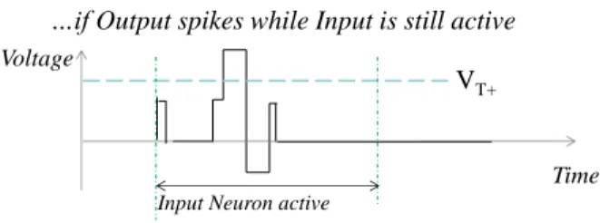
The disadvantage of the pulses of Figure 4 is the long input pulse which can be power hungry with some device technology. Figure 5 shows an alternative to these pulses, which is demanding lower power [14] for the cost of limited added complexity. The input neuron does not apply a voltage pulse during whole time it is active, but only at the beginning to drive current into the output neuron, and when a signal is sent back to it when one of the output neuron becomes active.
…if Output spikes while Input is still active
VT+ Voltage
Time
Input Neuron active
Figure 5. Low power variationof the pulses of Figure 4.
For device modeling, we use the model introduced and experimentally verified in [26] for memristive devices used as analog memories. An increase in the conductance is modeled by the equation: min max min G G G G
G
e
(1)Similarly, a decrease is modeled by: max max min G G G G
G
e
(2)Gmin and Gmax are the minimum and maximum
conductances of the nanodevices. + and _ characterize the
conductance step induced by each voltage pulse. + and - are
fitting parameters. The choice of all these parameters is inspired by the experimental measurements of [5] and is listed in Table I.
C. Results
Figure 6. Conductances learned in a simulation with 10 output neurons. Red is maximum cinductance (Gmax), blue is minimum conductance (Gmin).
For demonstration of the concept, in this paper we use the widely studied case of handwritten digits recognition. The MNIST database is used, which consists in 60,000 handwritten digits of 28x28 pixels by 250 writers [27]. Although this may not be the final application for our system, this constitutes the most studied problem in machine learning and is a mandatory step to evaluate our approach. In this paper, all simulations are system-level and are based on a C++ special purpose code (“Xnet”) [13], [15]. The code is event-based for simulation performance and runs on conventional CPUs. It simulates the equations of the network, using the voltage pulses shown in Figures 4 or 5.
40 50 60 70 80 90 100 2 104 6 104 1 105 1.4 105 1.8 105 100 10 output neurons 50 300
R
ec
o
g
n
iti
o
n
rat
e
(%
)
Iteration number during learning
(a) 40 50 60 70 80 90 100 0 100 200 300 400 500 Reco gni tion rate on the test ing s e t (% )Number of output neurons (b)
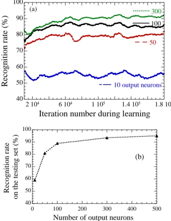
Figure 7. (a) Recognition rate during learning for simulations with different numbers of output neurons (from bottom to top: 10, 50, 100, 300). The recognition rates are running averages on 10,000 iterations. (b) Recognition
rate on the test dataset as a function of the numer of output neurons
In order to achieve learning, we present the full MNIST training database (60,000 digits) three times to the circuit. Each input neuron is connected with one pixel of the image. It emits spikes with a jittered rate that is proportional to the pixel intensity (Figure 2(b)). The initial phase is random. No kind of preprocessing on the digits is used and the set is not augmented with distortions. The network is then tested on the MNIST test database (10,000 digits), which consists in digits that have not been presented during training.
Figure 6 plots the conductances learned by the system in a configuration with only 10 output neurons. It is remarkable that without any supervision and using only our local custom STDP rule, the system has identified 9 (out of 10) different numbers, the real features of the input. Moreover it has
learned the distinctive features of the digits (and not just the most likely handwriting): it has learnt the loop of the digit two, the bottom of the six, or the horizontal parts of three and eight.
To evaluate the performance of the system, we can define a recognition rate. For that purpose, we associate output neurons with the digit for which they spike the most frequently a
posteriori. In hardware this association could be performed
with complex digital circuitry, and constitutes a difficulty. A satisfactory approach is presented in section IV of this paper, with the association of a supervised neural network.
A running average of the recognition rate during learning is shown in Figure 7(a). Whichever the number of output neurons, the network learns rapidly during the first 10,000 digit presentation and then keeps improving its performance gradually. The final performance is given as the mean recognition rate on the test database. It is actually higher than the performance on the training set seen in Figure 7(a), and is plotted in Figure 7(b). With ten output neurons the recognition rate reaches 60 %. For better performance, more output neurons are needed. With 50 output neurons the recognition rate reaches 81% and with 300 output neurons 93.5 %. A traditional artificial neural network with back-propagation with 300 hidden neurons (that has the same number of adjustable parameters) reaches 95 % [27], which compares to our rate of 93.5 %. In the literature, the best algorithm has a largely superior 99.7 % recognition rate, but has 12 million adjustable parameters (vs. 235,200 here) and uses a largely augmented training set [28]. Though our numbers are more modest, the interest here is that the network is fully unsupervised with extremely simple local learning rules.
The two variations of voltages pulses (Figures 4 and 5) gave identical performance in terms of recognition rate. All the results presented in the paper use the pulses of Figure 4.
Important, thanks to the unsupervised nature of learning, the complicated “labeling” step does not need to be performed right away. Lots of unknown data may be presented for training, and the labeling can be performed from a limited subset of well identified data. This is a strong advantage: for many problems involving natural data. Often, we have a lot of data, but that were not classified, and the system can here perform this analysis by itself.
D. Extreme robustness to device variations
One of the most important features of the unsupervised learning scheme is its extreme robustness to device variation. For every memristive devices, we considered variations in the parameters , of equations (1) and (2), the minimum
conductance Gmin, and the maximum conductance Gmax. To
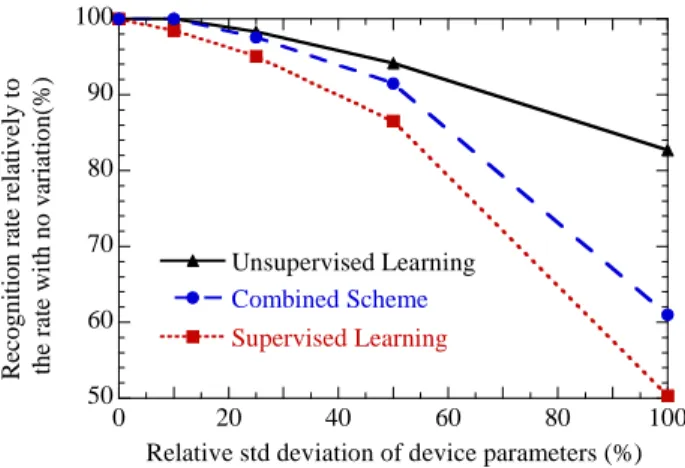
this purpose, we performed Monte Carlo simulations of our system, with all the parameters of all devices computed from a Gaussian probability law. Every simulation was repeated five times, and the average recognition rate is given. Figure 8 plots the degradation of the recognition rate, when device variation is increased. We see that the network is immune to variations up to 25% of the mean value of all these parameters, which constitutes an extremely high level of variation for an electron
device (but typical for research nanodevices [7], [8]). With 50% of variation, there is a small decrease of the recognition rate. With a dramatic variability of 100% on the synaptic parameters, the recognition rate decreases significantly, but interestingly the functionality of the network is not challenged. We should note that with a variability of 50%, 4% of the nanodevices cannot be programmed in at least one direction (i.e. they have an value of 0). The latter figure becomes 30% when parameter variability is 100%. This shows the overall tolerance to defects.
Figure 8 was computed for a system with 50 outputs. The results were similar for a system with 300 outputs (which appeared slightly more robust).
This degree of robustness to device variation is exceptional in electronic system and constitutes one of the strongest points of the approach. It takes root in the unsupervised nature of learning: output neurons learn features for which they are naturally “fit”. The variability is thus not a problem but a germ for learning. The extreme simplicity of the voltages pulses is also fundamental to ensure the robustness.
50 60 70 80 90 100 0 20 40 60 80 100 Unsupervised Learning Supervised Learning Combined Scheme R ec ogni ti on r at e r el at ivel y t o the r at e w it h no v ar iat ion( % )
Relative std deviation of device parameters (%) Figure 8. Robustness to devcie variation for the three schemes (unsupervised, supervised, combined). Degradation of the system’s recognition rate as a function of device variability. The variable parameters
are , , Gmin, Gmax.
III. SUPERVISED LEARNING SCHEME
A. Basic Principle
Using the same kind of nanodevices, a similar scheme may be developed to implement supervised learning, while retaining some variation insensitivity.
It is comparable to the unsupervised scheme and also uses the general architecture of Figure 1, but there is no voltage applied on the nanodevices when an output neuron spikes. The system works as follow. The input neurons present a digit during a given time, using one of the coding scheme of Figure 2. After this time period, input and output neurons apply a programming pulse on the nanodevices as illustrated on Figure 9. The input neurons apply a pulse only if they spiked during the period. The output neurons apply a voltage pulse depending on their situation, which can only program the
nanodevices in conjunction with a waveform on the input neuron end.
If the output neuron was expected to spike (it corresponds to the digit actually presented), the connections to the input neurons that spiked should be strengthened. The output neuron applies a negative spike that will strengthen the positive part of pre-synaptic pulses, and increase the conductances of nanodevices that present such pulses. If the output neuron was not expected to spike, inversely it should apply a positive pulse to weaken the synapses connected to input neurons that spiked. If the output neuron actually spiked (i.e. made a mistake) a pulse is applied to significantly reduce the conductances. If it did not spike (and thus was right) – which is the most typical situation – the pulse is lowered in order to only weakly weaken the conductances (and not cause the conductances to decrease too rapidly).
B. Results
A first test is to apply the scheme directly to the MNIST database. The parameters of the simulation are listed in Table I. The network performance on the testing set is 87.5%. The perceptron, a standard supervised neural network with similar complexity, has a performance of 88% [27].
If the input neuron spiked it applies….
If the output neuron was supposed to spike…
- but spiked
- and did not spike
If the output neuron was not supposed to spike…
Vinput Time Time Voutput Time Voutput Time Voutput
V
T+V
T-Figure 9. Voltage pulses used for supervised learning (voltage pulses as a function of time).
Thanks to the pass/fail approach a good variation to variability is achieved, although it is not as good as in the unsupervised scheme of section 3. With 10% variability on ,
, Gmin, Gmax performance (averaged on 5 runs) is reduced to
86.2%. With 25% variability it is reduced to 83.2%, and with 50% variability to 75.7%. This constitites impressive
robustness, but is actually not to the level of the unsupervised approach, as shown in Figure 8.
This scheme is not as robust as the previous one, because the system cannot decide which output neuron will learn which feature (this is imposed by the supervisor). Some memristive devices (connecting important pixels of the input to an output neuron) can thus play an important role. For relative standard variation of the characteristics above 50%, some devices become effectively nonfunctional, and in particular some of these important devices, causing a substantial decrease of the recognition rate.
If we compare with the unsupervised approach, the supervised one has the clear advantage of requiring less neurons and synapses, and to be simple to use. By contrast, it does not have its level of robustness to device variation. More important, it requires having every data used for training labeled since the system does not learn the distinguishable features itself as in unsupervised scheme, but based on the expected output.
IV. COMBINATION
We have proposed two schemes for designing learning-capable architectures with nanodevices. They are in fact compatible. To illustrate this we propose a two-crossbar architecture, illustrated in Figure 10. Every output of the unsupervised crossbar is fed as an input spike to the supervised crossbar. CMOS input neurons nanodevice CMOS output neurons (integrate & fire) CMOS neurons
(integrate & fire)
Unsupervised Crossbar
Supervised Crossbar
Figure 10. Architecture combining unsupervised and supervised crossbar
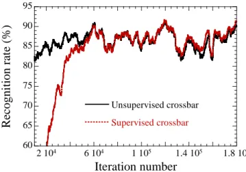
The role of the supervised layer is to label neurons trained by the unsupervised first layer of section II. It associates spikes on the output of the first layer with the actual digits presented. As illustrated on Figure 11, this works very well in practice. Until iteration 60,000 the supervised layer’s performance remains low, and then it matches the performance of the unsupervised layer, as calculated in section II. It can even become slightly become higher because the supervised layer is more adaptable than the majority rule used in section II.
Of particular interest, the problem solved by the supervised crossbar is simpler than by that of section III. This makes it less sensitive to device variations, as seen in Figure 8. Even
with variations of , , Gmin, Gmax of 25% the supervised
layer performance is matching perfectly the unsupervised layer very well. Starting with variations of 50%, the degradation of the recognition rate is slightly worse, but still better than in purely supervised problem of section III.
Globally, the supervision does not intrinsically improve the recognition rate, but provides a practical and flexible approach for the labeling operation. This opens up many opportunities. One ideal way to exploit the system is to first train the unlabeled layer on natural data, and then to perform a “labeling” on a small training set by activating the supervised layer. This works very well in the case of our MNIST dataset and identical recognition rate is obtained as with training the supervised layer with all the data when the supervised layer is trained with as little as 2,000 digits. This could be a useful way to process all kinds of natural data. We may collect tons of video, auditory and olfactory data and feed it to our adaptable electronic system. It would learn distinguishable features thanks to the unsupervised layer. Then a quick training with well identified data of the supervised layer can provide the system’s functionality.
60 65 70 75 80 85 90 95 2 104 6 104 1 105 1.4 105 1.8 105 Unsupervised crossbar Supervised crossbar
Reco
gni
tion
rat
e (%)
Iteration number
Figure 11. Two layer learning. Learning rate of the second (labeling) layer trained by variability compatible supervision (red) compared with learning of the first layer (black), as computed in the previous section. Variability of 10%
on all parameters (initial conductances, , ,Gmin, Gmax)
TABLE I. PARAMETERS USED IN THE SIMULATIONS
Unsupervised Crossbar
With conductances in normalized units (Gmax=1):
= 10-2, = 5.10-3, wmin = 10 -4,
max
w = 1,
+ = 3.0, - = 3.0, the input pulses are 25 ms long, the output pulses 0.5 ms (as inspired by [5]). Neurons
parameters are taken from [13]. When a variability of X%, is applied on a parameter, it means that the standard deviation of the parameter
is X% of its mean value.
Device variability is always applied to Gmax, Gmin,
, Supervised
Crossbar
Same as unsupervised. For the weak conductance reduction = 5.10-4
V. CONCLUSION AND PERSPECTIVES
We have presented two different learning approaches to exploit memristive nanodevices as synapses in neuroinspired systems. The STDP-based unsupervised approach can learn based on unlabeled data and has extreme tolerance to device variation (relative standard deviation of 50% may be tolerated on all significant device parameters). The supervised approach is simple to program but needs labeled data, and is not as tolerant. Both approaches can be combined, which opens the way of first training the system on a large dataset, and then of training the supervised layer on a small labeled subset to identify what has been learnt. In this situation, an excellent robustness to device variation is achieved.
Such works highlight the credibility of the new computing paradigm associating neuroinspired systems and nanoelectronics, to provider “smarter” electronics, especially for embedded applications where the ability to process natural data efficiently and in real time can be particularly useful. Future works will focus on experimental demonstration beyond single device that we have already achieved [14] and new applications like video [15], auditory or olfactory data processing or the inference in complex databases. More complex networks, with several unsupervised layers will also be considered.
ACKNOWLEDGMENT
The authors would like to thank S. J. Thorpe, P. Dollfus, M. Suri and B. DeSalvo for fruitful collaboration.
REFERENCES
[1] M. Versace and B. Chandler, “The brain of a new machine,” IEEE
Spectrum, vol. 47, no. 12, pp. 30–37, 2010.
[2] D. S. Modha, R. Ananthanarayanan, S. K. Esser, A. Ndirango, A. J. Sherbondy, and R. Singh, “Cognitive computing,” Communications of
the ACM, vol. 54, p. 62, Aug. 2011.
[3] D. B. Strukov, G. S. Snider, D. R. Stewart, and R. S. Williams, “The missing memristor found,” Nature, vol. 453, no. 7191, pp. 80–83, Mai 2008.
[4] G. Agnus, W. Zhao, V. Derycke, A. Filoramo, Y. Lhuillier, S. Lenfant, D. Vuillaume, C. Gamrat, and J.-P. Bourgoin, “Two-Terminal Carbon Nanotube Programmable Devices for Adaptive Architectures,” Adv.
Mater., vol. 22, no. 6, pp. 702–706, 2010.
[5] S. H. Jo, T. Chang, I. Ebong, B. B. Bhadviya, P. Mazumder, and W. Lu, “Nanoscale Memristor Device as Synapse in Neuromorphic Systems,” Nano Lett., vol. 10, no. 4, pp. 1297–1301, Avril 2010. [6] J. V. Arthur and K. Boahen, “Learning in silicon: Timing is
everything,” Advances in neural information processing systems, vol. 18, p. 281–1185, 2006.
[7] S. H. Jo and W. Lu, “CMOS Compatible Nanoscale Nonvolatile Resistance Switching Memory,” Nano Lett., vol. 8, no. 2, pp. 392–397, Février 2008.
[8] J. Borghetti, G. S. Snider, P. J. Kuekes, J. J. Yang, D. R. Stewart, and R. S. Williams, “`Memristive’ switches enable `stateful’ logic operations via material implication,” Nature, vol. 464, no. 7290, pp. 873–876, Avril 2010.
[9] G.-Q. Bi and M.-M. Poo, “Synaptic modification by correlated activity: Hebb’s Postulate Revisited,” Annu. Rev. Neurosci., vol. 24, no. 1, pp. 139–166, Mar. 2001.
[10] G. S. Snider, “Spike-timing-dependent learning in memristive nanodevices,” in Prof. of IEEE International Symposium on Nanoscale
Architectures 2008 (NANOARCH), 2008, pp. 85–92.
[11] D. Kuzum, R. G. D. Jeyasingh, B. Lee, and H.-S. P. Wong, “Nanoelectronic Programmable Synapses Based on Phase Change Materials for Brain-Inspired Computing,” Nano Letters, vol. 12, no. 5, pp. 2179-2186, 2012.
[12] Shimeng Yu, Yi Wu, R. Jeyasingh, D. Kuzum, and H. P. Wong, “An Electronic Synapse Device Based on Metal Oxide Resistive Switching Memory for Neuromorphic Computation,” IEEE Transactions on
Electron Devices, vol. 58, no. 8, pp. 2729–2737, Aug. 2011.
[13] D. Querlioz, O. Bichler, and C. Gamrat, “Simulation of a memristor-based spiking neural network immune to device variations,” Proc. of the
Int. Joint Conf. on Neural Networks (IJCNN), pp. 1775 – 1781, 2011.
[14] M. Suri, O. Bichler, D. Querlioz, O. Cueto, L. Perniola, V. Sousa, D. Vuillaume, C. Gamrat, and B. DeSalvo, “Phase change memory as synapse for ultra-dense neuromorphic systems: Application to complex visual pattern extraction,” in International Electron Devices Meeting
Technical Digest (IEDM), 2011, pp. 4.4.1–4.4.4.
[15] O. Bichler, D. Querlioz, S. J. Thorpe, J.-P. Bourgoin, and C. Gamrat, “Extraction of temporally correlated features from dynamic vision sensors with spike-timing-dependent plasticity,” Neural Networks, vol. 32, pp. 339-348, Aug. 2012
[16] J. H. Lee and K. K. Likharev, “Defect-tolerant nanoelectronic pattern classifiers,” Int. J. Circ. Theor. Appl., vol. 35, no. 3, pp. 239–264, May 2007.
[17] S.-Y. Liao, J.-M. Retrouvey, G. Agnus, W. Zhao, C. Maneux, S. Fregonese, T. Zimmer, D. Chabi, A. Filoramo, V. Derycke, C. Gamrat, and J.-O. Klein, “Design and Modeling of a Neuro-Inspired Learning Circuit Using Nanotube-Based Memory Devices,” IEEE Transactions
on Circuits and Systems I: Regular Paper , vol. 58, no. 9, p. 2172-2181,
Sep. 2011.
[18] D. Chabi, W. Zhao, D. Querlioz, and J.-O. Klein, “Robust neural logick block (NLB) based on memristor crossbar array,” Proc. of IEEE/ACM
Int. Symp. Nanoscale Architectures (NANOARCH 2011), pp.
137-143,2011.
[19] A. Gorchetchnikov, M. Versace, H. Ames, B. Chandler, J. Leveille, G. Livitz, E. Mingolla, G. Snider, R. Amerson, D. Carter, H. Abdalla, and M. S. Qureshi, “Review and unification of learning framework in Cog Ex Machina platform for memristive neuromorphic hardware,” in
Neural Networks (IJCNN), The 2011 International Joint Conference on,
2011, pp. 2601 –2608.
[20] S. O. Haykin, Neural Networks: A Comprehensive Foundation, 2nd ed. Pearson, 1997.
[21] J. Liang and H.-S. . Wong, “Cross-Point Memory Array Without Cell Selectors—Device Characteristics and Data Storage Pattern Dependencies,” IEEE Trans. Electron Devices, vol. 57, no. 10, pp. 2531–2538, Oct. 2010.
[22] E. Linn, R. Rosezin, C. Kugeler, and R. Waser, “Complementary resistive switches for passive nanocrossbar memories,” Nat Mater, vol. 9, no. 5, pp. 403–406, mai 2010.
[23] P. Lichtsteiner, C. Posch, and T. Delbruck, “A 128× 128 120 dB 15 μs Latency Asynchronous Temporal Contrast Vision Sensor,” IEEE
Journal of Solid-State Circuits, vol. 43, no. 2, pp. 566–576, 2008.
[24] V. Chan, S.-C. Liu, and A. van Schaik, “AER EAR: A Matched Silicon Cochlea Pair With Address Event Representation Interface,” IEEE
Trans. Circuits Syst. Regul. Pap., vol. 54, no. 1, pp. 48–59, 2007.
[25] P. Merolla, J. Arthur, F. Akopyan, N. Imam, R. Manohar, and D. S. Modha, “A digital neurosynaptic core using embedded crossbar memory with 45pJ per spike in 45nm,” in Custom Integrated Circuits
[26] D. Querlioz, P. Dollfus, O. Bichler, and C. Gamrat, “Learning with memristive devices: how should we model their behavior?,” Proc. of
IEEE/ACM Int. Symp. Nanoscale Architectures (NANOARCH 2011),
pp. 150-156, 2011.
[27] Y. Lecun, L. Bottou, Y. Bengio, and P. Haffner, “Gradient-based learning applied to document recognition,” Proceedings of the IEEE, vol. 86, no. 11, pp. 2278–2324, 1998.
[28] D. C. Ciresan, U. Meier, L. M. Gambardella, and J. Schmidhuber, “Deep Big Simple Neural Nets Excel on Handwritten Digit Recognition,” CoRR abs/1003.0358, Mar. 2010.