HAL Id: tel-01092812
https://tel.archives-ouvertes.fr/tel-01092812v3
Submitted on 16 Dec 2014
HAL is a multi-disciplinary open access
archive for the deposit and dissemination of sci-entific research documents, whether they are pub-lished or not. The documents may come from teaching and research institutions in France or abroad, or from public or private research centers.
L’archive ouverte pluridisciplinaire HAL, est destinée au dépôt et à la diffusion de documents scientifiques de niveau recherche, publiés ou non, émanant des établissements d’enseignement et de recherche français ou étrangers, des laboratoires publics ou privés.
Quantum Cutting Processes in Rare-earth doped
fluorides for Photovoltaic applications
Diana Serrano
To cite this version:
Diana Serrano. Quantum Cutting Processes in Rare-earth doped fluorides for Photovoltaic applica-tions. Materials Science [cond-mat.mtrl-sci]. Université de Caen Basse-Normandie, 2012. English. �tel-01092812v3�
U.F.R. DES SCIENCES ECOLE DOCTORALE S.I.M.E.M.
THESE Présentée par
Diana SERRANO GARCÍA
Et soutenue Le 28 Septembre 2012
En vue de l’obtention du
DOCTORAT de l’UNIVERSITE de CAEN Spécialité : Milieux dilués et optique fondamentale
Arrêté du 07 août 2006
Quantum cutting processes in rare-earth doped
fluorides for photovoltaic applications
MEMBRES DU JURY:
Mme Fabienne PELLE, Dir. de Recherche CNRS, LCMCP, Chimie ParisTech (rapporteur) Mr Bernard MOINE, Dir. de Recherche CNRS, LPCML, Lyon I (rapporteur)
Mr Xianghua ZHANG, Dir. de Recherche CNRS, EVC, Sciences Chimiques de Rennes Mr Richard MONCORGE - Professeur, CIMAP, Université de Caen (co-directeur) Mr Alain BRAUD - Maître de Conférences HDR, CIMAP, Université de Caen (directeur)
Remerciements v
List of Abbreviations vii
Résumé 1
Introduction 9
1 Current context and challenges 13
1.1 PV technologies . . . 13
1.2 First Generation: Silicon wafers . . . 14
1.3 Second generation: thin-film technologies . . . 15
1.3.1 Hydrogenated amorphous Silicon based technologies . . . 16
1.3.2 CdTe, CIS and CIGS thin films . . . 17
1.3.3 Dye-sensitized solar cells (DSSCs) and organic photovoltaic (OPV) devices . . . 18
1.3.4 III-V semiconductors for high-efficiency PV devices . . . 19
1.4 Third-generation photovoltaics . . . 20
1.4.1 Fundamental limitations of current PV technologies . . . 21
1.4.2 Multi-bandgap approaches: high-efficiency multi-junction solar cells and Quantum wells solar cells (QWSCs) . . . 23
1.4.3 Modifying the solar spectrum . . . 24
1.4.4 Concentrated Photovoltaics (CPV) . . . 27
1.5 RE based converters for silicon solar cells efficiency enhancement . . . 28
1.5.1 Energy levels of rare-earth ions in crystals . . . 28
1.5.2 Energy transfer processes . . . 32
1.5.3 Rare-earth based solar up and down converters . . . 33
1.6 Conclusions Chapter 1 . . . 44 i
ii Contents 2 Quantum Cutting in Pr3+-Yb3+ codoped KY
3F10 47
2.1 Introduction . . . 47
2.2 Experimental methods . . . 49
2.3 Optical spectroscopy experiments . . . 51
2.3.1 Emission spectra . . . 52
2.3.2 Decay curves . . . 56
2.4 First energy transfer efficiency . . . 58
2.5 Second energy transfer and quantum efficiency . . . 59
2.6 Rate equation modeling . . . 60
2.6.1 Steady-state solutions . . . 63
2.6.2 Dynamic solutions . . . 67
2.6.3 Conclusions . . . 72
2.7 Other modeling approaches . . . 73
2.7.1 Rate-equation limitations . . . 73
2.7.2 Inokuti-Hirayama model . . . 74
2.7.3 Monte Carlo (MC) methods . . . 75
2.7.4 Modeling Result . . . 77
2.7.5 MC methods incorporated to the population rate-equations . . . 78
2.8 Conclusions Chapter 2 . . . 81
3 Clusters and energy transfers in CaF2:Pr3+-Yb3+ 83 3.1 Introduction . . . 83
3.2 Rare-earth clustering in CaF2: general concepts . . . 84
3.2.1 Single ions sites . . . 85
3.2.2 Higher order aggregates or clusters . . . 87
3.3 Experimental methods . . . 90
3.4 Quantum cutting with CaF2: Pr3+-Yb3+ . . . 91
3.4.1 CaF2:Pr3+-Yb3+ spectroscopy . . . 91
3.4.2 Determination of the first energy transfer efficiency . . . 96
3.5 Preliminary conclusions and next challenges . . . 98
3.6 Spectroscopy of the Pr3+ aggregates in CaF 2 . . . 98
3.6.1 Weak luminescence of Pr3+ ions in CaF 2 . . . 98
3.6.2 Pr3+-Yb3+ and Pr3+-Lu3+ codoping . . . 100
3.7 Pr3+-Yb3+ and Pr3+-Lu3+ clusters . . . 107
3.7.1 Elimination of Pr3+ clusters . . . 107
3.7.2 Evidence of two types of clusters in the codoped samples . . . 108
3.8 Lifetimes and ETE in the ultra-fast clusters . . . 114
3.8.1 Super-exchange interaction . . . 114
3.8.2 Fast Cluster to Ultrafast Cluster ratio . . . 116
3.8.3 Consequences . . . 118
3.9 Summary of results . . . 119
3.10 QC with Pr3+-Yb3+ codoped CaF 2: Yb3+ emission and modeling . . . 120
3.10.1 Yb3+ emission and lifetimes . . . 120
3.10.2 Rate-equation modeling . . . 124
3.11 Conclusions Chapter 3 . . . 127
4 Cooperative Quantum Cutting in CaF2:Tb3+-Yb3+ 129 4.1 Introduction . . . 129
4.2 Experimental methods . . . 130
4.3 Spectroscopy of the Tb3+-Yb3+ clusters in CaF 2 . . . 131
4.3.1 Tb3+ aggregates . . . 131
4.3.2 Tb3+-Yb3+ spectroscopy . . . 133
4.3.3 Yb3+ emission . . . 134
4.3.4 Lifetimes and ETE . . . 136
4.4 Conclusions . . . 139
4.5 Sensitization . . . 140
4.5.1 Tb3+ ions sensitization . . . 142
4.5.2 CaF2 codoped Tb3+-Ce3+ and Tb3+-Bi3+ investigation . . . 145
4.6 Absolute QC efficiency in Pr3+-Yb3+ and Tb3+-Yb3+ doped CaF 2 . . . 147
4.6.1 Experimental protocol . . . 147
4.6.2 Absorbed power measurement . . . 148
4.6.3 Downconverted Yb3+ emission and absolute QE . . . 151
4.6.4 discussion . . . 153
4.7 Conclusions Chapter 4 . . . 155
General conclusions 157
iv Contents
List of figures 191
Une thèse est sans doute un travail de recherche, mais elle constitue aussi une grande formation. C’est pour cela que je tiens à remercier tout particulièrement Alain Braud pour avoir encadré cette thèse. Le grand appui et les nombreux enseignements qu’il m’a offert depuis mon arrivé au laboratoire ont été d’un grand enrichissement autant scientifique que personnel. Je tiens également à remercier Richard Moncorgé pour m’avoir accueilli dans son équipe de recherche, pour l’intérêt porté à mon travail et pour son soutien. Je voudrais témoigner ensuite ma plus sincère gratitude pour Jean-Louis Doualan, Patrice Camy, Abdel Benayad et Vivien Ménard, dont la collaboration a été aussi nécessaire que précieuse pour qu’une thèse comme celle-ci puisse aboutir. Merci à Jean Margerie, avec qui j’ai eu l’honneur de pouvoir travailler, pour partager avec moi un peu de son immense savoir et expérience. Enfin, je voudrais remercier M. Serge Bouffard pour m’avoir accueilli dans le laboratoire CIMAP aussi que pour son soutien au projet du Student chapter.
Pendant ces années j’ai eu la chance de rencontrer un grand nombre d’amis, dont la présence et compagnie est devenue très importante pour moi. Ainsi, je voudrais dédier un mot à Burcu. Merci pour ta compagnie, tes réflexions et tes bons conseils dont j’espère profiter toujours. Un grand merci aussi à Thomas et Kiki. Merci pour partager avec moi votre univers de fous, pour les rires, et pour faire maintenant partie de beaucoup de moments inoubliables. Je remercie Delphine pour son amitié, Philippe pour les sourires; Julie pour les discussions et conseils; Oliv Deb pour être lui même et en générale tous ce qui m’ont accompagné pendant cette aventure. J’ai passé des moments excellents avec vous. Merci à mes amis Elsa, Bertrand, Sheila, Luis et Arantxa. Je souviendrai le temps que nous avons passé tous ensemble comme la meilleur période de ces trois ans. A Marta, Miriam et Pilar pour faire preuve chaque jour que la distance n’existe pas pour les gens qui s’apprécient. A mes parents, pour le support qui rend simple ce qui est compliqué et même des fois, possible, ce qui est impossible.
• a.Si:H - Hydrogenated Amorphous Silicon • c-Si - Crystalline Silicon
• CPV - Concentrated Photovoltaics • CTB - Charge Transfer Band • CW - Continuous waveform • DC - Downconversion
• DSSC - Dye-Sensitized Solar Cell • ESA - Excited State Absorption • ET - Energy Transfer
• ETE - Energy Transfer Efficiency • ETU - Energy Transfer Upconversion • GSA - Ground State Absorption
• HIT - Heterojunction with Intrinsic Thin Layer • IH - Inokuti-Hirayama
• LD - Laser Diode • LT - Low Temperature
• LQY - Luminescence Quantum Yield • LPE - Liquid Phase Epitaxy
viii Abbreviations • MBE - Molecular Beam Epitaxy
• mc-Si - Multicrystaline Silicon • MC - Monte-Carlo
• MEG - Multiple Electron Generation • MPE - Multiple Photon Emission
• MOVPE - Metalorganic Vapour Phase Epitaxy • NIR - Near-Infrared
• nc-Si - Nanocrystaline Silicon • µc-Si - Microscrystalline Silicon • OPV - Organic Photovoltaics
• PLE - Photoluminescence excitation • PMMA - Poly(methyl methacrylate) • PV - Photovoltaic
• QC - Quantum Cutting
• QCE - Quantum Cutting Efficiency • QD - Quantum Dot
• QE - Quantum Efficiency
• QWSC - Quantum Well Solar Cell • QDSC - Quantum Dot Solar Cell • RE - Rare-earh
• SPR - Surface Plasmon Resonance • TCO - Transparent Conducting Oxide • RT - Room Temperature
Depuis que l’existence de matériaux luminescents avec des efficacités quantiques supérieures à l’unité fut mis en évidence, de nombreuses recherches ont été consacrées à l’étude des mécanismes physiques conduisant à l’émission de plusieurs photons de faible énergie à partir de l’absorption d’un seul photon d’énergie supérieure. Ce phénomène, habituellement connu comme “quantum cutting”, a été mis en évidence dans des matéri-aux tels que les solides inorganiques, les semi-conducteurs et les molécules organiques. Parmi les matériaux solides luminescents, les matériaux dopés terres rares sont ceux qui présentent le plus grand potentiel pour le quantum cutting et ses applications. Ces ions lu-minescents ont été tout d’abord étudiés à cause de leurs propiétés optiques remarquables. Pourtant, cela ne fut que depuis la découverte du laser, dans les années 60, que l’intérêt pour les terres rares trivalentes augmenta jusqu’à ce qu’il fut étendu à d’autres applica-tions dans le domaine de l’optique et la photonique. A l’heure actuelle, les ions terres rares se trouvent dans des très nombreux systèmes optiques tels que les amplificateurs, les mémoires quantiques et les guides d’onde entre autres.
Les recherches sur le quantum cutting ont commencé par l’étude de matériaux dopés terres rares présentant une émission en cascade. L’intérêt s’est ensuite focalisé sur des couples de terres rares où l’énergie peut-être transférée d’un des ions, appelé donneur, vers le deuxième (accepteur) par le biais d’un seul ou plusieurs processus de transferts d’énergie. Le quantum cutting a trouvé une de ses premières applications dans le développement de phosphores sans mercure pour des applications d’éclairage [102]. Depuis quelques années, le mécanisme du quantum cutting est apparu comme étant prometteur pour l’amélioration du rendement des cellules solaires à base de silicium cristallin.
Les technologies photovolta¨ıques sont habituellement classifiées en trois générations [6]. La première génération, qui est celle des cellules solaires à base de silicium cristallin, a été la première commercialement disponible et représente encore aujourd’hui plus de 90% du marché photovolta¨ıque mondial. La deuxième génération photovolta¨ıque, comprenant
2 Résumé des technologies tels que le silicium amorphe [12], les cellules CIS et CIGS [26] ou les semi-conducteurs III-V [11] est basée sur le développement les techniques de couches minces. Dans cette seconde génération, le coût de production diminue notablement par rapport à la première génération grâce à la réduction de la quantité de semi-conducteur utlilisée dans les modules photovolta¨ıques. Malheureusement une diminution importante du ren-dement de conversion accompagne cette réduction de l’épaisseur du semi-conducteur. Les efficacités record sont actuellement de l’ordre de 25% [8] pour les cellules à base de silicium cristallin mais sont largement inférieures pour les technologies de deuxième génération. Afin d’augmenter les rendements de conversion tout en gardant des côuts de production faibles, la troisième génération photovolta¨ıque comprend plusieurs approches, une des plus importantes étant la possibilité d’utiliser des convertisseurs luminescents capables de transformer l’énergie des photons solaires incidents pour adapter le rayonnement solaire à l’absorption des cellules solaires silicium. En effet, pour toute technologie solaire basée sur une seule junction semi-conductrice, des pertes intrinsèques limitent l’efficacité des modules. Ces pertes, qui fixent le rendement maximale pour une cellule silicium à 29% [34], sont issues d’une part de l’absence d’absorption pour les photons d’énergie inférieure au gap du semi-conducteur (1.12 eV dans le cas du silicium cristallin) et d’autre part sont liées aux effets de thermalisation qui ont lieu après l’absorption de photons d’haute énergie. Un convertisseur dit “basse-frequence” placé en surface de la cellule (Fig.1) qui soit capable de transformer chaque photon de haute énergie en deux photons d’énergie égale à la moitié du photon original, et idéalement, de l’ordre de la bande interdite du silicium, permettrait donc de réduire les pertes provoquées par les effets de thermalisation en générant de deux électrons dans la bande de conduction par photon incident.
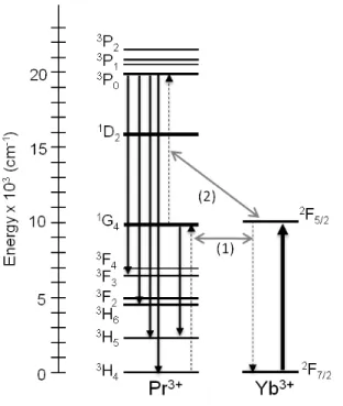
Dans ce travail de thèse des matériaux dopés terres rares sont étudiés en tant que quantum cutters efficaces pour le développement de convertisseurs solaires basse-fréquence. Avec cet objectif, le codopage Pr3+-Yb3+ a été étudié dans les matériaux
hôtes KY3F10 et CaF2. Ce codopage présente un schéma de niveaux d’énergie
perme-ttant le quantum cutting à partir de deux transfert d’énergie résonants et consécutifs, le premier transfert étant Pr3+(3P
0→1G4);Yb3+(2F7/2→2F5/2) et le deuxième transfert
Pr3+(1G
4→3H4);Yb3+(2F7/2→2F5/2) (Fig.2).
Figure 2: Schéma du quantum cutting pour le système Pr3+-Yb3+.
L’efficacité des deux transferts d’énergie décrits dépend de plusieurs paramètres parmis lesquels les plus importants sont la distance entre les ions donneurs et accepteurs et le recouvrement spectral entre l’émission du donneur et l’absorption de l’accepteur (Eq.1).
WDA =
CDA(n)
Rn (1)
Une série d’échantillons de KY3F10 et CaF2, avec la même concentration en Pr3+ (0,5%)
et des concentrations en Yb3+ différentes ont été fabriqués en utilisant la technique de
Bridgement-Stockbarger (Tableau 1). Les fluorures tels que KY3F10 et CaF2
4 Résumé non-radiative en favorisant le rendement de fluorescence des terres rares et en général, l’efficacité des mécanismes de transfert d’énergie.
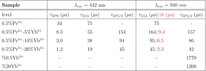
Table 1: Concentration disponibles pour les échantillons de KY3F10 et CaF2 codopés
Pr3+-Yb3+. KY3F10 CaF2 0.5%Pr3+ 0.5%Pr3+ 0.5%Pr3+-1%Yb3+ 0.5%Pr3+-0.5%Yb3+ 0.5%Pr3+-5%Yb3+ 0.5%Pr3+-1%Yb3+ 0.5%Pr3+-10%Yb3+ 0.5%Pr3+-2%Yb3+ 0.5%Pr3+-20%Yb3+ 0.5%Pr3+-4%Yb3+ 0.25%Pr3+ 0.5%Pr3+-10%Yb3+
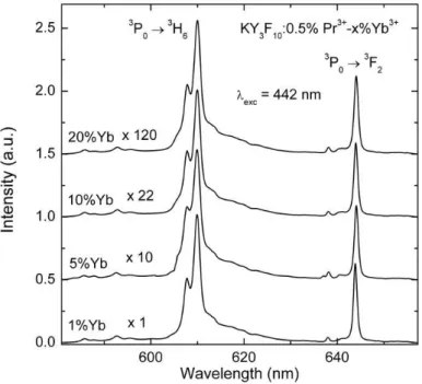
Des valeurs d’efficacité de transfert d’énergie peuvent être facilement calculées pour le premier transfert d’énergie dans les différents échantillons de KY3F10 (Tableau 2) à
partir des valeurs exprérimentales obtenues pour la durée de vie du niveau 3P 0:
Table 2: Efficacité du premier transfert d’énergie pour les échantillons de KY3F10codopés
Pr3+-Yb3+.
Echantillon Efficacité du transfert (%)
KY3F10:0.5%Pr3+-5%Yb3+ 75,6
KY3F10:0.5%Pr3+-10%Yb3+ 91,4
KY3F10:0.5%Pr3+-20%Yb3+ 96,4
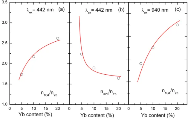
L’étude de l’efficacité pour le deuxième transfert d’énergie apparait quant à elle beaucoup plus compliquée. Un modèle d’équations de population classique a été devel-oppé et comparé aux expériences pour les différents échantillons de KY3F10:Pr3+-Yb3+.
A partir de la modélisation nous pouvons déduire la valeur du taux de transfert pour les différents mécanismes de transfert d’énergie qui ont lieu dans le système (Tableau 3). La modélisation confirme d’ailleurs l’existence d’un équilibre thermique entre les niveaux 1G
4 and 2F5/2 et donc, l’existence de transferts d’énergie dans les deux sens i.e.
Pr3+(1G
4)→Yb3+ et Yb3+→Pr3+(1G4). Le modèle met de plus en évidence l’existence de
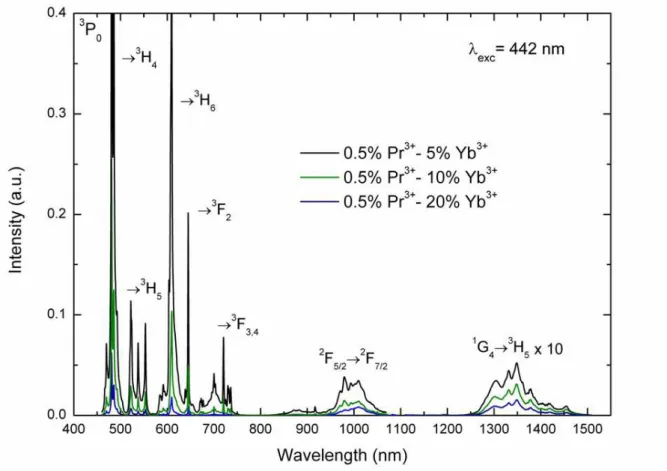
et donc l’efficacité du quantum cutting pour l’émission de deux photons autour de 1 µm. En revanche, une augmentation des émission infrarouges du Pr3+ (1.3 µm et 2 µm) est
observée, issue des transissions 1G
4→3H5 and 3H6→3H4.
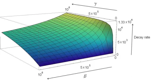
Table 3: Taux de transfert déduits de la modélisation où α représente le premier transfert d’énergie, β le deuxième transfert et γ et δ des mécanismes de dépeuplement de l’Yb3+.
Echantillon α(s−1) β(s−1) γ(s−1) δ(s−1)
KY3F10:0.5%Pr3+-5%Yb3+ 8.94×10⁴ 1.05×10⁴ 2.52×10³ 5.05×10³
KY3F10:0.5%Pr3+-10%Yb3+ 3.28×10⁵ 2.10×10⁴ 5.05×10³ 1.00×10⁴
KY3F10:0.5%Pr3+-20%Yb3+ 8.08×10⁵ 4.21×10⁴ 1.01×10⁴ 2.02×10⁴
L’étude du codopage Pr3+-Yb3+ dans CaF
2 montre que les taux de transfert et
les efficacités des transfert qui ont pu être mesurées sont encore beaucoup plus élevées dans ce matériau hôte (Tableau 1). Bien que des taux de transfert de 96,4% ont été mis en évidence pour le premier transfert d’énergie avec un échantillon de KY3F10 codopé
0.5%Pr3+-20%Yb3+ (Tableau 2), l’efficacité de ce même transfert d’énergie dans le cas des
échantillons de CaF2:Pr3+-Yb3+ est remarquablement supérieure (jusque’à 99.97% pour
CaF2 codopé 0.5%Pr3+-10%Yb3+). Cette différence est expliquée par l’existence d’une
distribution de dopants complètement différente entre les deux matériaux hôtes. Ainsi, le dopage de KY3F10avec des ions terres rares donne lieu à une distribution uniforme d’ions
dans la matrice tandis que dans le cas de CaF2, la formation de clusters de terres rares
au sein desquels la distance entre les ions est très courte (seulement quelques Å) rend les transferts d’énergie plus efficaces dans ce matériau.
Les clusters résultant du codopage de CaF2 avec Pr3+ et Yb3+ ont été analysés
en détail. Les études spectroscopiques mettent en évidence l’existence de trois types de centres différents. Ces centres sont identifiés comme étant des ions Pr3+ isolés, des
clusters de Pr3+ au sein desquels les mécanismes de rélaxation croisée sont très efficaces
ce qui rend la luminescence des ions Pr3+ dans ces clusters très faible, et finalement, des
clusters de Pr3+-Yb3+ présentant des transferts d’énergie du Pr3+ vers l’Yb3+ extêmement
efficaces. Deux types de clusters de Pr3+-Yb3+ ont été ensuite distingués. Chaque cluster
est caractérisé par un spectre d’émission différent et de plus, par des taux de transfert contrastés. Ainsi, un taux de transfert de l’ordre de 105 s−1 est mesuré pour un premier
type de clusters, dits “rapides”, tandis qu’un taux de transfert de l’ordre de 107 s−1 est
6 Résumé en particulier dipôle-dipôle, rend compte du taux de transfert obtenu pour les clusters “rapides” (Eq.1). Ce n’est pas le cas pour les clusters “ultra-rapides” dont le taux de transfert ne peux pas être expliqué que par une interaction de type échange où le taux de transfert présente une dépendance exponentielle avec la distance entre les ions (Eq.2) ce qui donne lieu à des taux de transferts beaucoup plus élevés. Ce résultat indique une différence structurelle importante entre les deux types de clusters, les distances entre les ions dans les clusters “ultra-rapides” étant nécessairement beaucoup plus courtes que dans les clusters “rapides”.
Wex = 1 τ0exp(γ(1 − R R0 )) (2)
Figure 3: Evolution des espèces avec la concentration en Yb3+.
En utilisant de nombreux résultats expérimentaux originaux, les proportions des différents centres (Pr3+ isolés; clusters de Pr3+ et clusters de Pr3+-Yb3+) ont pu être
déterminées en fonction de la concentration en Yb3+. Ainsi, seulement les clusters de
Pr3+-Yb3+ existent pour des concentrations égales ou supérieures à 4%Yb3+, étant les
clusters “ultra-rapides” devenant rapidement dominants avec une proportion de 84% par rapport au nombre total de centres luminescents pour une concentration de 10%Yb3+.
Au contraire, les clusters de Pr3+ dominent la structure à faibles concentrations
en Yb3+. Cette analyse nous permet de conclure que ce sont les échantillons avec des
concentrations supérieures à 4% qui vont être finalement intéressants pour le quantum cutting (Fig.3) bien que l’extinction de la luminescence de l’Yb3+ soit aussi constatée dans
CaF2 à hautes concentrations en Yb3+.
Les différents études réalisées autour des clusters de Pr3+-Yb3+ ont révélé l’existence
d’une équivalence spectroscopique entre le codopage Pr3+-Yb3+ et le codopage Pr3+-Lu3+
dans CaF2. Le codopage Pr3+-Lu3+ donne ainsi lieu au même type de clusters que le
codopage Pr3+-Yb3+, ce qui est dû aux similarités existantes entre l’Yb3+ et le Lu3+
(masse et rayon atomique). Le codopage avec Lu3+ conduit au remplacement des clusters
de Pr3+ par des clusters de Pr3+-Lu3+ tel qu’il est observé dans la Figure 3. Par contre,
l’absence de transfert d’énergie du Pr3+ vers le Lu3+, contrairement à l’Yb3+, provoque
une augmentation drastique de la luminescence dans ce codopage. En particulier, la luminescence est 400 fois plus intense dans CaF2 codopé 0.5%Pr3+-5%Lu3+ par rapport à
CaF2simplement dopé 0.5%Pr3+. La luminescence étant très faible dans CaF2simplement
dopé Pr3+, l’utilisation de ce matériau laser ce trouve limitée, ce qui n’est pas le cas pour
le codopage Pr3+-Lu3+.
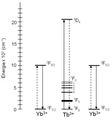
8 Résumé Le mécanisme du quantum cutting a été finalement étudié avec le codopage Tb3+
-Yb3+ dans CaF
2. Dans ce système, l’excitation de deux Yb3+ a lieu par le biais d’un seul
transfert d’énergie dit coopératif à partir du niveau 5D
4 du Tb3+ (Fig.4). Le mécanisme
coopératif est plusieurs ordres de grandeur moins efficace qu’un transfert d’énergie réso-nant. Pourtant, les études spectroscopiques réalisées accomplies avec une série d’échantillons de CaF2 codopés Tb3+-Yb3+ indiquent la formation de clusters de Tb3+-Yb3+ au sein
desquels le transfert coopératif est particulièrement efficace. Les valeurs obtenues pour l’efficacité du transfert coopératif ainsi que pour l’efficacité du quantum cutting sont présentées dans le Tableau 4. Contrairement au comportement observé dans le codopage Pr3+-Yb3+, la luminescence de l’Yb3+ augmente avec la concentration en Yb3+ pour le
système Tb3+-Yb3+, ce qui indique l’absence de mécanismes de dépeuplement de l’Yb3+
dans ce matériau et confirme l’intérêt de ce système pour l’application envisagée.
Table 4: Efficacité du premier transfert d’énergie pour les échantillons de CaF2 codopés
Tb3+-Yb3+.
Echantillon Efficacité du transfert (%) Efficacité du QC
CaF2:0.5%Tb3+-0.5%Yb3+ 18 118
CaF2:0.5%Tb3+-2%Yb3+ 22 122
CaF2:0.5%Tb3+-10%Yb3+ 47 147
CaF2:0.5%Tb3+-20%Yb3+ 53 153
L’étude du rendement absolu du quantum cutting pour les échantillons de CaF2
codopés Pr3+-Yb3+et Tb3+-Yb3+montre une efficacité 40 fois supérieure pour le codopage
Tb3+-Yb3+. Malgré ce résultat prometteur, un défi reste à résoudre concernant la faible
absorption du niveau5D
4 du Tb3+ (σabs∼10−23 cm2). Différents candidats sont ainsi
con-siderés pour la sensibilisation du Tb3+ dont la bande 5d du Ce3+. Une étude préliminaire
a été réalisée qui montre l’existence d’un transfert d’énergie efficace du Ce3+ vers le Tb3+
Since the existence of luminescent materials presenting quantum efficiencies greater than unity was first demonstrated, several investigations have been devoted to the study of the physical mechanisms leading to the generation of several low-energy photons per incident high-energy photon. This phenomenon, usually referred to as quantum cutting, is nowadays known to occur in different materials such as inorganic solids, semiconductors and organic molecules.
Among the luminescent solids, rare-earth doped materials have shown a remarkable potential for quantum cutting applications. These luminescent ions were first studied at the beginning of the last century because of their peculiar properties. However, it was after the discovery of the laser action in the early 60s that the interest in trivalent rare earth ions grew up and was also extended to optics and photonics applications other than lasers. Therefore, rare-earth ions can be currently found in various optical systems such as optical amplifiers, quantum memories and waveguides.
Investigations on quantum cutting started with singly rare-earth doped-materials capable of a cascade emission. The focus was next shifted to the combination of two rare-earth ions where the energy of one of them, usually referred to as donor, is transferred stepwise to the other one (acceptor) through a single or a series of energy transfers. The quantum cutting mechanism found one of its first applications in the development of effi-cient Hg free rare-earth doped phosphors for the lighting industry which led to an intense research activity on potential quantum cutters. More recently, quantum cutters appear to be able to notably contribute to the next generation of photovoltaic (PV) technolo-gies by converting UV-visible photons into several near-infrared (NIR) photons in order to minimize the energy losses due to thermalization of electron-hole pairs in the PV modules. This thesis is focused on the study of rare-earth doped fluoride materials presenting a strong potential for visible to infrared quantum cutting:
10 Introduction In Chapter 1, the main photovoltaic technologies are reviewed paying particular attention to the so-called third generation approaches. The aim of the PV third-generation is to reduce production costs while increasing the efficiency of the cells. Among these approaches, improving the silicon cells efficiency is planned by using rare-earth doped luminescent converters able to shift the visible-near UV incident solar radiation to the near-infrared region so as to adapt the incident light to the silicon layer absorption.
The second half of the first chapter recalls the theoretical background leading to the determination of the energy levels of rare-earth ions in crystals. The principal energy transfer theories are next summarized finishing the chapter by a detailed review of the potential rare-earth based luminescent solar converters reported so far in the literature. These systems are presented as classified within two types, namely upconverters when referring to systems able to perform an energy shift from low energy to higher energy; and downconverters, when transforming instead high energy into lower energy.
Chapter 2 presents the investigation of the quantum cutting mechanism in Pr3+
-Yb3+ codoped KY
3F10. The energy transfers taking place within the Pr3+-Yb3+ system
are here studied by a series of optical spectroscopy experiments, along with a classical rate equation modeling. Energy transfer rate values as well as quantum efficiency values are deduced from the rate equation modeling concluding that the energy transfers from Pr3+
to Yb3+ions occur in an efficient way. However, the Yb3+ emission appears to be strongly
quenched because of efficient back-transfer mechanisms taking place from Yb3+ to Pr3+
ions. A further description of the Pr3+ and Yb3+ dynamics is carried out by using
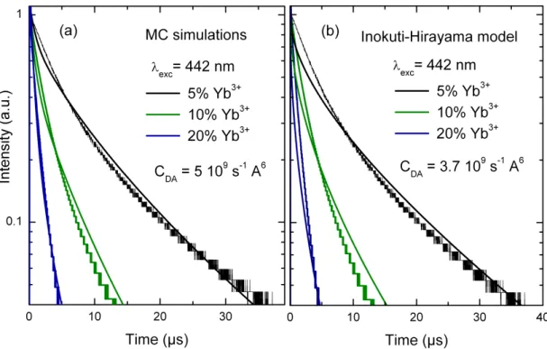
mod-eling approaches such as the Inokuti-Hirayama model and Monte-Carlo computational methods. The Monte-Carlo methods are demonstrated to present a strong potential for modeling dynamics involving energy transfers.
In Chapter 3, the quantum cutting mechanism is investigated with a series of CaF2:Pr3+-Yb3+ samples. The spectroscopic study reveals first the existence of two
dif-ferent Pr3+ centers within the CaF
2:Pr3+-Yb3+codoped crystals. These species are
identi-fied as isolated Pr3+ ions and Pr3+-Yb3+ clusters. A dominance of the Pr3+-Yb3+ clusters
is clearly observed when increasing the Yb3+ concentration in the sample. High energy
transfer efficiencies for the first energy transfer are determined in CaF2:Pr3+-Yb3+ due to
The second part of this chapter presents a further insight into the rare-earth clus-tering in CaF2. Singly Pr3+ doped CaF2 is dominated by non-luminescent Pr3+ clusters
which explain the very weak emission observed for this material. On the contrary, the codoping of Pr3+ ions with Lu3+ions avoids the formation of the Pr3+ clusters and instead
favors the emergence of Pr3+-Lu3+ clusters which emit light. The Pr3+-Lu3+ codoping
is then compared to the Pr3+-Yb3+ codoping concluding that they give rise to the same
type of rare-earth aggregates. Moreover, this investigation evidences the existence of two different types of Pr3+-RE3+ clusters (with RE3+= Lu3+ or Yb3+). These two types of
clusters are primarily distinguished by their emission spectrum and, in the case of the Pr3+-Yb3+ codoping, by their energy transfer rate and associated energy transfer
mech-anism. Indeed, the energy transfer from Pr3+ to Yb3+ in the so-called fast Pr3+-Yb3+
cluster is most likely due to a dipole-dipole interaction. On the contrary, in the so-called ultra-fast cluster, the energy transfers are demonstrated to be far more efficient, which is attributed to a super-exchange interaction. The results derived from the detailed spectro-scopic study enable a more complete evaluation of the QC mechanism in CaF2:Pr3+-Yb3+
by taking into account the impact of the ultra-fast clusters, previously unnoticed, in the energy transfer efficiencies.
Chapter 4 is devoted to the study of the cooperative quantum cutting mechanism with Tb3+-Yb3+ codoped CaF
2. The spectroscopic investigations show the formation of
Tb3+-Yb3+ clusters within which the cooperative energy transfer is particularly efficient.
On the other hand, the analysis of the evolution of the Yb3+ emission with the Yb3+
con-tent reveals a promising low impact of the Yb3+ quenching in CaF
2:Tb3+-Yb3+. The last
part of the chapter is focused on the RE3+ sensitization. The potential Tb3+ sensitizers
are finally reviewed including some promising and very recent results obtained with Ce3+
1
Current context and challenges
1.1
PV technologies
Nowadays, it is widely accepted that human activities contribute to climate change. The activities devoted to energy production are those which present the highest environ-mental impact. Carbon dioxide emissions due to burning fossil fuels increased by 53% from 1971 to 2008 [1] and, during the same period, the world surface temperature and sea level raised [2]. Coincidence or not, these types of climate change evidences, combined with the growing global energy demand, are important incentives for the development of CO2 neutral and renewable energy industries.
The term “solar energy” refers in a general way to any use of sunlight radiations for practical ends. The sun constitutes an endless source of energy whose applications are indeed multiple. For instance, the sun is a natural source of lighting, and also, so-lar radiations can be used to directly heat air, water or even cook. These soso-lar passive technologies reduce the need for alternate resources limiting thus CO2 emissions.
How-ever, besides these support technologies, solar active technologies are devoted to increase the world’s energy supply. Electrical power generation is possible with materials able to produce a voltage upon exposure to light. Those materials undergo the well-known photovoltaic effect so that, they are usually referred to as photovoltaic (PV) materials. Up until now, PV energy only represents a small contribution to the world total primary energy supply. Nevertheless, the growth rate in terms of cell production is impressive, with 27.2 GW manufactured within the year 2010, which constitutes a growth rate of 118%, the greatest annual growth in 12 years [3]. In agreement with this tendency, the International Energy Agency (IEA) [4] claims that solar power generators may produce most of the world′s electricity within 50 years, dramatically reducing the emissions of
greenhouse gases that harm the environment. Unfortunately, in spite of these global per-13
14 1.2. First Generation: Silicon wafers spectives, the costs associated with the PV energy production must still be reduced in order to enter areas of competitiveness so far unknown.
Since Russell Ohl accidentally discovered the first solar cell in 1940 (US Patent 2402662) [5], numerous materials have been investigated as potential PV devices giving rise to the current variety of solar technologies. One of the pioneer in solar cell technology, Professor Martin Green, classified the PV devices within three main generations, setting crystalline silicon wafer-type cells as PV first generation, thin-films technologies as a second generation, and any new concepts leading to improve the solar cells performance and competitiveness, in an heterogeneous third generation [6]. This classification is widely accepted nowadays.
Figure 1.1: First Silicon cell by Bell laboratory [7].
1.2
First Generation: Silicon wafers
The first solar cell was developed in 1940 but it was after the 1950′s semiconductors
revolution that the first efficient solar cell and its first commercial application appeared [7]. That primitive device made of a silicon wafer was able to convert 6% of the sun-light radiation into electricity (Fig.1.1). Since then, wafer-type silicon cells, which can be monocrystalline (c-Si) or multicrystalline (mc-Si) depending on the manufacturing tech-nique, have remained essential to PV technologies. From that low efficiency primitive device, the PV first generation has evolved to the current c-Si cells with 24.7% efficiency [8]. These wafer-type c-Si cells hold the world record efficiency among the overall single-junction technologies. Multicrystalline Si cells are indeed less efficient (19.3% [9]) than
those made from a Si single crystal. However, they have also known success since they are much simpler to produce and far less expensive to manufacture, presenting durability and longevity comparable to their monocrystalline counterparts.
During the past fifty years, crystalline and multicrystalline silicon have remained the main PV materials despite several studies pointing that other materials could become good PV candidates. Wafer-type crystalline silicon PV modules (consisting of a number of joint c-Si solar cells) were the first devices commercially available and still represent the most mature technology so that they continue to dominate the PV energy market with a share between 80 and 90 percent in 2010 (52.9% of monocrystalline and 33.2% of multicrystalline) even though the research and development of new PV technologies has notably intensified in recent years [3].
In general terms, the first generation of solar cells is successful. However, the c-Si wafer-type cells do not offer optimal performance, which should include stability, dura-bility and high efficiency combined with economical viadura-bility. Within the manufacturing costs, the price of the Silicon wafer constitutes the largest cost, with more than 50% of the global expenses [10]. This is the reason why the development of thin-film technologies opened a new way to achieve low-cost PV devices.
Figure 1.2: First generation cell (left). Second generation cell (right).
1.3
Second generation: thin-film technologies
First generation wafers are made from a cut of a silicon ingot. In the second gen-eration, the semiconductor is deposited onto a substrate glass, plastic or steel (Fig.1.2). These technologies save costs by reducing the waste of the precious semiconductor. How-ever, not only the costs but also the efficiency rates are limited in the so-called second generation (from 22.9% for a first generation c-Si module to 8.2% in a second
genera-16 1.3. Second generation: thin-film technologies tion 1-2 µm thin-film mc-Si submodule [11]) The balance between price and efficiency is without question the main challenge for the PV second generation.
1.3.1
Hydrogenated amorphous Silicon based technologies
Hydrogenated amorphous silicon (a-Si:H), introduced in the mid-1970′s, appeared
to be the best material for low-cost devices. Hydrogenated amorphous silicon cells use less than 1% of the silicon needed for a classical c-Si solar cell. Moreover, a-Si:H is a better absorber since its absorption coefficient exceeds by almost one order of magnitude that of c-Si over the 315-750 nm range [12]. Nevertheless, the adoption of this technology has been impaired by a problem of inherent instability, named the Staebler-Wronski effect after its discoverers [13], which provokes the cell efficiency to drop during the first six months of operation. As of this day, despite a better understanding of the effect, a solution has not been found. The current record efficiency for stabilized laboratory a-Si:H p-i-n1
cells is around 10% [14]. In the mid-1990′s, many research groups started to optimize
the first stages of crystallization of their a-Si:H films. This led to the development of nanocrystalline (nc-Si) silicon and microcrystalline silicon (µc-Si) films consisting of small crystalline grains (l0-500 Å) embedded in an amorphous silicon matrix. The use of these specific films to trigger the ordering process is now known to result in more stable and more efficient devices [16]. Currently, researches on a-Si are mainly focused on stacked structures such as a-Si/µc-Si, or a-Si/nc-Si (so-called “micromorph” tandem cells) [16]. Up to date, the record efficiency for this PV technology has been achieved with an a-Si/nc-Si/nc-Si tandem cell presenting 12.5% efficiency [17].
The a-Si/c-Si heterojunction (Fig.1.3), also known as HIT (Heterojunction with Intrinsic Thin layer), constitutes an interesting alternative within the a-Si technologies. It is formed by depositing extremely thin layers of intrinsic and doped a-Si:H onto a c-Si wafer. It is a simple process with relatively low manufacturing costs which gives rise to promising solar cells with improved efficiency [18]. The potential of this technology was definitely demonstrated by Sanyo in 1991 [19]. Since then, it has been continuously developed reaching outstanding efficiency results in both research laboratory cells (22% efficiency [20]]), and commercial modules (19.5% efficiency [21]).
1A p-i-n junction is a varied form of the standard p-n junction, formed at the boundary between a
p-type (lack of electrons or hole excess) and n-type (electron excess) semiconductor, in which, an intrinsic part of semiconductor is introduced between the p-zone and n-zone
Figure 1.3: HIT cell [22].
PV technologies based on a-Si:H are low-cost, light, flexible (a 1 µm thin-film can be deposited onto a flexible substrate) and with aesthetical success so that their major applications are architectural structures (solar cell roof shingles [23]) and little devices (calculators, watches, lanterns. . . ). In addition, the good efficiency results obtained with a-Si/c-Si heterojunctions (HIT) make this a-Si based technology a potential candidate for energy supply.
1.3.2
CdTe, CIS and CIGS thin films
CdTe cells dominated the first 25 years of thin-film PV technologies. Having a nearly ideal energy bandgap for a single-junction solar cell (1.41 eV at 300 K [24]), efficient CdTe cells were fabricated by different potentially scalable low-cost processes in the past. The best results showed efficiencies of 16.7% for CdTe research cells [11] and 10.9% for modules [25]. However, the usual problem associated with CdTe technologies is its acceptance in the market place. For the time being, cadmium and tellurium are not expensive materials but the availability of tellurium could become a serious inconvenience since it is an extremely rare element. In addition, Cd is toxic if ingested, inhaled or handled improperly so that manufacturing processes must be done in precise safety conditions, eventually rising the production costs.
The ternary alloy CuInSeCO2 (CIS) was also found to exhibit properties well suited
for PV converters. It is a direct band-gap semiconductor presenting a high optical absorp-tion, stable electro-optical properties and energy bandgap suited for PV applications. In the seventies, the tandem CdS/CuInSeCO2/Mo showed 12% efficiency [26]. Since then,
the structure has been under continuous development. Firstly, CIS evolved into an alloy, Cu(In,Ga)Se2 (CIGS). Progressively, the CIGS layer and the other components taking
18 1.3. Second generation: thin-film technologies part in the tandem evolved resulting in more and more efficient devices. Currently, CIGS cells present a complex stacked structure with a record efficiency of 20% [27]. Despite the good efficiency results, CIGS manufacturing remains a complex and expensive process. Current researches on CIGS try to solve these challenges, for example, by looking for low-cost deposition methods in order to avoid expensive vacuum processes [28], with the aim of providing economical viability to this PV technology.
1.3.3
Dye-sensitized solar cells (DSSCs) and organic photovoltaic
(OPV) devices
In the early 1960′s, it was discovered that many common dyes had semi-conducting
properties. Later, these dyes were among the first organic materials to exhibit PV effect [29]. In a dye sensitized solar cell (DSSC) (Fig.1.4) light absorption generates excitons (electron-hole pairs travelling as a unit). Then, the pair is separated when reaching a boundary which is, in this case, the interface between the dye and the Ti02 layer [20]. So
far, DSSCs have achieved efficiencies around 11% with research cells [31].
Figure 1.4: Gratzel-type DSSC scheme. Once separated, the Ti02 layer captures the
DSSCs cells have been in development for a relatively long period compared to other PV approaches. Most in the PV community associate the problems and issues of DSSCs with the dye itself. Dyes are expensive and, in addition, the liquid dye and the solid-liquid interface present doubts about their long-term viability. A low cost manufacturing perspective is considered as the main advantage of this PV technology. However, DSSCs remain under development; therefore, they are still far from reaching the commercial market to be able to prove their competitiveness. Besides dyes, the PV effect has been observed in many important biological molecules such as carotenes, chlorophylls and other porphyrins [29]. Also based on excitonic processes, only a few of these organic photovoltaic (OPV) devices have validated performance and still, in a very low efficiency range (3-5%). As DSSCs, the major support of this technology has always been the possibility of reaching extremely low cost devices. Organic semiconductors are a less expensive alternative than inorganic semiconductors and, in addition, organic molecules can be processed by a large number of cheap techniques which are not available to crystalline inorganic semiconductors [32]. In spite of that, the OPV approach has many challenges to overcome before becoming a real alternative in the PV market. A very recent result (December 2011), by Heliatek, a Germany-based developer of organic photovoltaic cells, is nevertheless particularly encouraging for the future of OPV cells. Heliatek has achieved 9.8% of certified efficiency. This device shows indeed far better efficiency than any other OPV device investigated so far, pointing that the major disadvantage of OPV cells i.e. the low efficiency, might be overcome in the future.
1.3.4
III-V semiconductors for high-efficiency PV devices
Binary, ternary and quaternary alloys such as GaAs, GaAlAs and GaInAsP, have been receiving a special attention in recent years because of their potential as PV convert-ers. According to the latest report, single junction GaAs thin-film research cells exhibit 27.6% efficiency [11], which is the absolute efficiency record within the thin-film technolo-gies. In addition, these cells show greater conversion efficiency than the most efficient first generation c-Si wafer-type cells. On the other hand, as it happens with CIGS cells, the economical viability of this technology has always been questioned due to the expen-sive deposition techniques needed for their production. Nevertheless, the interest in these compounds for solar applications has been renewed since they give rise to one of the most important third generation approaches: the extremely efficient multi-junction solar cells.
20 1.4. Third-generation photovoltaics
1.4
Third-generation photovoltaics
The optimal PV device should present reliability, high efficiency and low cost. The PV second generation tried to reduce costs by limiting the waste of raw material and by looking for cheap processing techniques. The cost reduction resulted in less efficient PV devices (around 10% efficiency for a-Si:H, CdTe, DSSCs and OPVs). On the other hand, more efficient solutions have been proposed (CIGS, III-V single-junction cells), although they present the disadvantage of being expensive. With the aim of achieving high efficiency and low manufacturing costs at the same time (Fig.1.5), the third generation tackles new approaches. Most of these approaches are nowadays in the first steps of research and development, however, they are expected to play a fundamental role in the future PV technologies [6,33].
Figure 1.5: Efficiency and cost projections for first (I), second (II), and third generation (III) PV technologies (wafer-based, thin films and advanced approaches respectively). The first and second generation efficiency limit range (denoted single bandgap limit) is represented for solar concentrated power [34].
1.4.1
Fundamental limitations of current PV technologies
For any solar cell based on a single p-n junction, the upper conversion efficiency the device will be able to achieve is determined by the loss mechanisms taking place within the semiconductor. Four major loss mechanisms exist in a standard solar cell: lack of absorption for below bandgap photons; losses due to thermalization mechanisms after absorption of photons in the excited states of the conduction band; losses related to the junction and contact voltage, and finally, losses due to the recombination of electron-hole pairs within the junction (Fig.1.6). Between these four mechanisms, two of them i.e. absence of below bandgap photons absorption and thermalization, significantly limit the conversion efficiency of the resulting device. Recombination losses are indeed unavoidable, but their impact can be neglected in comparison with other loss mechanisms. On the other hand, the contact voltage and junction losses can be notably reduced with well-designed devices.
Figure 1.6: Band diagram representing the four types of loss processes in a standard p-n junction: (1) Non absorption of below bandgap photons; (2) lattice thermalization losses; (3) and (4) junction and contact voltage losses; (5) recombination losses (radiative recombination is unavoidable).
Taking in account sub-bandgap transparency and thermalization losses; assuming zero contact resistance and considering the sun as a black emitting body (Fig.1.7), Shock-ley and Queisser investigated the detailed balance limit of efficiency for single junction solar cells [34]. This limit is a theoretical upper value which establishes the maximum achievable ratio between the number of extracted electrons and the number of incident photons in a semiconductor under non concentrated sunlight radiation.
22 1.4. Third-generation photovoltaics
Figure 1.7: AM1.5 Solar radiation spectrum
Shockley and Queisser obtained a limiting efficiency of 31% for a 1.3 eV bandgap optimized cell. Silicon and GaAs cells, with bandgaps of 1.12 eV and 1.45 eV respectively (Table 1.1), present the same efficiency limit (29% [34]). Thus, the record efficiencies reported in each case, i.e. 24.7% for first generation c-Si cells [8] and 27.6% for second generation GaAs thin films [11], indicate well-designed and technologically developed devices approaching their upper efficiency limit.
The detailed balance limit eventually shows that single junction solar cells are only efficient to convert solar photons within a small energy range located around the semi-conductor bandgap energy. Thus, the solar spectrum, emitting between 250 and 2500
Table 1.1: Main PV semiconductors bandgap energies. PV cell bandgap (eV) λ (nm)
CdS 2.4 516 a-Si 1.75 711 CdTe 1.56 790 GaAs 1.45 860 CIGS 1.41 880 c-Si 1.12 1100
nm (Fig.1.7) is clearly underexploited by first and second generation single junction cells. The aim of the third generation PV approaches is to go through the theoretical limit and, for that, a more efficient exploitation of the solar spectrum is required.
1.4.2
Multi-bandgap approaches: high-efficiency multi-junction
solar cells and Quantum wells solar cells (QWSCs)
Derived from the second-generation III-V single junction cells, multiple junction PV cells are among the few high-efficiency technologies that have been realized and commer-cialized. These devices, also referred to as tandem cells, are based on a stacking of p-n junctions, each junction, tuned to a specific energy of the solar spectrum as displayed in Fig.1.8. III-V semiconductors are particularly suitable for this technology due to their bandgap adjustability. Thus, the GaInP/GaAs/Ge triple-junction cell presents confirmed efficiency of 32% under one-sun2 radiation [11]. A larger number of junctions assure,
in principle, a better exploitation of the solar spectrum. Concepts of 4-6 junctions are now in the research stage [35] although each layer added entails tremendous technological complexities due to the lattice mismatch between the different semiconductors. There-fore, translating such a complex device from the laboratory to the commercial market, nowadays, is not a real option. This kind of technology can find its application in the spatial industry [36] for which the efficiency is a priority unlike costs.
Figure 1.8: Absorption mechanism in a triple-junction solar cell. From the front side to the rare side, the layers follow a decreasing bandgap energy order. Above-bandgap photons are progressively absorbed by the consecutive layers while sub-bandgap photons reach the next layer.
24 1.4. Third-generation photovoltaics Quantum wells solar cells (QWSCs) constitute an advanced approach to multi-bandgap solar cells derived from the recent development of semiconductor nanostructures [37,38]. The PV device is based on a single p-i-n structure with a number of narrow low bandgap regions or quantum wells (QWs), within the intrinsic zone of the junction. The QWs can be created by intercalating very narrow films (a few nanometers) of a lower bandgap semiconductor into the main semiconductor; or, by a semiconductor quan-tum dots (QDs) structure as displayed in Fig.1.9. These QWSCs are also referred to as Quantum dots solar cells (QDSCs). The main advantage of this structure is its enhanced absorption. Contrarily to single-junction solar cells, in QWSCs, sub-bandgap photons can be absorbed by the wells. Optimally, carriers escape next from the well (thermal escape) so that, the light absorbed by the cell in the lower bandgap regions is integrally converted into photocurrent before recombining [39]. QWSCs are based on a complex technology which could provide good efficiency results in the future. As a proof, efficiencies of 26% have been measured with a GaAsP/GaInAs nanostructured PV device [40]. Nevertheless, the biggest inconvenient of this technology is still the price of the resulting device, since it involves expensive materials and deposition methods (MBE, MOVPE. . . ).
Figure 1.9: QDs solar cell.
1.4.3
Modifying the solar spectrum
So far, we have presented third-generation technologies trying to accommodate the PV cell absorption to the solar energy range. However, instead of tuning the device absorption, modifying the incoming spectrum can be realized by incorporating energy
conversion layers or spectral converters, into existing solar cells [41-44]. Thus, a first converter could be placed on top of the solar cell for downconversion (frequency shift from high energy to lower energy), while a second layer could be placed at the back of the cell for upconversion (frequency shift from low energy to higher energy), both layers being electronically isolated from the active semiconducting layer.
Figure 1.10: (a) solar cell with downconverter added to the front side; (b) solar cell with upconverter on the rear side.
The aim of the downconversion layer (downconverter) is to split high energy photons into several lower energy photons in order to create several electron-hole pair per incident photon. This splitting, usually referred to as quantum cutting, allows a more efficient use of the incident photon energy since it reduces thermalization losses. The downconverter must be placed on the front side of the cell to be able to convert the incident photons before they reach the semiconducting layer (Fig.1.10.a). On the other hand, the role of the upconversion layer (upconverter), is to combine several non absorbable low energy photons to create a single higher energy photon with energy above the semiconductor’s bandgap energy. Since the purpose of an upconverter is to use photons transmitted by the cell, it can be placed at the rear side with a good optical coupling necessary to ensure high transmission of the low energy light to the upconverter and of the upconverted light back into the cell (Fig.1.10.b). Thus, the major loss mechanisms in single-junction solar cells (thermalization and non absorption of low energy photons), are expected to be reduced by these two layers. Indeed, the Shockley and Queisser upper efficiency limit is estimated to be increased from 29% [34] to 40.2% for a c-Si cell with an upconversion layer incorporated [45]; and from 29% to 36.6% for a c-Si cell with a downconversion layer [43]. In addition, the advantage in comparison to other PV technologies is that no modification of the active layer is needed, and neither a complicated cell structure such as that used for tandem solar cells or QWSCs. In conclusion, this alternative tries to implement already existing PV technologies, particularly c-Si based technologies, enhancing their efficiency but restraining costs by taking advantage of already developed manufacturing techniques.
26 1.4. Third-generation photovoltaics In a general way, a spectral converter must fulfil characteristics such as wide ab-sorption bands, emission peaks matching the solar cell abab-sorption, minimum reabsorp-tion losses due to overlap of absorpreabsorp-tion and emission spectra, luminescent quantum yield (LQY) near unity, high transmittance in the cell’s high response region and low scattering. Some candidates are:
Fluorescent organic dyes
Organic luminescent materials such as perylene-based dyes exhibit near-unity LQY [46] and have been demonstrated stable for many years in a PMMA host [47]. In the eighties, multi-dye systems were proposed to increase the absorption range of solar cells [48] since they were shown to be able to absorb up to 70% of the solar spectrum energy [49]. Downconversion processes take place in these compounds by cascade emission when the emission of one molecule is absorbed and re-emitted by another molecule that has a longer emission wavelength. Thus, photons absorbed at shorter wavelengths travel through the different luminescent dyes to be finally emitted by the longest wavelength emitting dye [50]. The main disadvantage is that multidye plates exhibit narrow absorption bands as well as significant reabsorption losses [51].
Luminescent semiconductor quantum dots (QDs)
The development of spectral converters containing semiconductor nanocrystals or QDs is also investigated [52]. Semiconductor QDs present broad absorption spectra with high absorption coefficients opening the door to an extensive utilization of the solar spec-trum energy [53]. In addition, QDs technologies provide spectral tunability since their absorption and emission characteristics are controlled by the QD diameter [54]. The possibility of multiple exciton generation (MEG) within the QDs also exists [55]. MEG is a process during which an electron with kinetic energy larger than the semiconductor bandgap energy excites a second electron from the valence band creating two electron-hole pairs. This phenomenon has been observed recently with PbSe QDs resulting in LQY up to 3 [56]. This means that every PbS QD in the sample produces three electron-hole pairs per incident photon so that each absorbed photon eventually results in the emis-sion of three lower energy photons. Currently available semiconductor QDs only exhibit LQYs lower than 1, reabsorption losses and instability. However, they will present a great potential as energy converters if stable and high LQY systems become more available.
Rare-earth ions
Lanthanides or rare earth ions is the name used to refer to a group of elements with atomic number comprised between 57 (Lanthanum) and 71 (Lutetium). Usually presented as doubly or triply charged ions, these elements are also referred to as 4f elements since they can be recognized by their unfilled and optically active 4f shell. Generally, as luminescent centers within a host material, trivalent rare-earth ions exhibit stability, small reabsorption losses and high LQY. In addition, the 4f energy levels offer a large variety of energy transfer possibilities between different rare-earth ions [57]. Thus, rare-earth doped materials are good candidates both for upconversion and downconversion quantum cutting. Unfortunately, as a disadvantage, trivalent rare earth ions present narrow absorption peaks with low absorption coefficients. The summary of properties presented in Table 1.2, shows that rare-earths seem to be the best suited luminescent species for solar cells efficiency enhancement by energy conversion approaches [58]
Table 1.2: Comparison of the potential energy converters main properties.
Desired property Dyes QDs REs
Wide absorption band × √ ×
Minimal reabsorption × × √
High LQY √ × √
Stability √ × √
1.4.4
Concentrated Photovoltaics (CPV)
Solar concentrators do not constitute a PV technology, however, they must be men-tioned since they can be considered as a promising complement for any existing PV technology. Solar concentrators have been studied since the seventies and nowadays, they are implemented in many PV installations for power supply. Typically formed by lenses and mirrors, their purpose is to focus a large area of sunlight radiation into a small area of PV material. Therefore, solar concentrators increase the amount of incident energy consequently increasing the electric output of the device. In addition, CPV systems are not expensive and lead to a reduction of the PV cells size, which is particularly interest-ing to limit the costs in high-efficiency technologies such as multi-junction solar cells. For
28 1.5. RE based converters for silicon solar cells efficiency enhancement instance, the GaInP/GaAs/InGaAs triple-junction cell holds the absolute world record of efficiency with 42.3% confirmed efficiency under 406 suns concentrated light [59]. For comparison, the upper efficiency limit for a c-Si solar cell with an upconversion layer un-der concentrated sunlight is calculated to be 54% [45]. This theoretical value represents an increase of almost 200% in comparison to the classical Shockley-Queisser limit (29%), which proves that solar concentrators may be playing a major role in the future when combined with third-generation PV technologies.
1.5
RE based converters for silicon solar cells efficiency
enhancement
As seen in a previous section, silicon PV technologies, comprising c-Si, mc-Si and a-Si:H devices, dominate the current solar energy market with more than 90% of world trade. In addition, the research stage and high costs of other PV technologies combined with the secure supply of raw silicon for the next decades, and the possibility of making the already existing Si cells more efficient through third-generation approaches such as downconversion and upconversion layers acting under concentrated sunlight, points that silicon will remain the dominant PV technology in the future.
Among the luminescent species proposed for modifying the solar spectrum, it was shown that trivalent rare-earth ions were the ones which fitted best the required properties. In this section, we review some fundamental concepts on rare-earth ions acting as dopants within a crystalline environment, and then, we describe the different rare-earth doped systems investigated as third-generation upconverters and downconverters for silicon solar cells efficiency enhancement.
1.5.1
Energy levels of rare-earth ions in crystals
The energy states of a free-atom with n electrons are given by the time-independent Schrödinger equation:
Hψ(r1, ..., rn) = Eψ(r1, ..., rn) (1.1)
in which ψ(r1, ..., rn) is the wavefunction of eigenvalue E, and H, is the Hamiltonian for
H = n X i=1 (−~ 2 2m∇ 2 − Ze 2 4πǫ0ri ) + n X i=1 ξ(ri)lisi+ 1 2 n X i=1 n X j=1 e2 4πǫ0|ri− rj| (1.2)
The many-electron Hamiltonian is composed of three terms, the first term being a sum over n electrons of one-electron kinetic and potential energy operators; the second term representing the spin-orbit coupling interaction and the third one describing the inter-electron Coulomb repulsion [60]. Approximated wavefunctions can be found for the n-electron system under central field approximation. This approximation assumes that the inter-electron repulsion term contains a large spherically symmetric component referred to as U(ri)). Thus, H = H0+ H′+ Hso (1.3) in which H0 = n X i=1 (−~ 2 2m∇ 2 − Ze 2 4πǫ0ri ) + U (ri) (1.4) Hso = n X i=1 ξ(ri)lisi (1.5) H′ = 1 2 n X i=1 n X j=1 e2 4πǫ0|ri− rj| − n X i=1 U (ri) (1.6)
For atoms with low atomic number the effect of H′ is greater than that of H
so so that
wavefunctions, namely LS terms of energy E(2S+1L) are found for H
0 + H′. The
spin-orbit interaction is next taken in account (LS coupling or Russel-Saunders coupling), provoking the degenerated2S+1L terms to split into several 2S+1L
J terms with J = L + S
and degeneracy equal to 2J + 1 [61]. On the other hand, atoms with high atomic number, endure the effect of the spin-orbit interaction more than that of H′. In that case, we
consider the coupling of the spin and orbital angular momentum on individual electrons (j states with j = j + s for individual electrons) and then, the coupling of the j states through H′ (j-j coupling).
Eventually, wavefunctions are more complicated to determine when the effect of H′
is comparable to that of Hso since a mixing of states with the same quantum number
J and different quantum numbers L and S takes place (intermediate coupling). The rare-earth ions belong to this group. The 4fn energy levels are thus expressed as 2S+1L
30 1.5. RE based converters for silicon solar cells efficiency enhancement Russel-Saunders terms, their final position is then derived from experimental data of the free-ion emission spectra. The 4fn energy levels were reported by Dieke and Crosswhite
in 1963, being the results summarized in the so-called Dieke diagram [57]. In the presence of a crystal environment, the 2S+1L
J levels split into a number of
sub-levels (Stark sub-levels) due to the interaction between the 4fn electrons and the
electric field created by the ions forming the crystal lattice. For the particular case of dopant rare-earth ions, the optically-active 4f electrons are only weakly affected by the crystal field since they are partially screened by the filled 5s25p6 outer shells. Thus, the
splitting due to the spin-orbit coupling is much stronger than the splitting provoked by the interaction with the crystal field (Hcf) (Fig 1.11), which is thus treated as a perturbation
on the free-ion energy levels:
H = H0+ H′ + Hso+ Hcf (1.7)
Figure 1.11: 4f energy levels splitting under the effect of different interactions. The study of the crystal field is a very complex problem. The simplest description uses the point charge model, in which, the lattice ions causing the electrostatic crystal field are represented by point charges supposed fixed in their lattice position. The crystal-field Hamiltonian takes then the form:
Hcf = 1 4πǫ0 n X i=1 n X l=1 Zle2 |Rl− ri| (1.8)
where the summations is done over all 4f electrons and ligands. The development of |Rl− ri|−1 in a base of spherical harmonics leads to:
Hcf = X k,q X l BkqCqk(θ, φ) (1.9)
which is the form of the crystal field usually employed for rare-earth ions, with Bk q the
crystal field parameters. The crystal field experienced by the optically-active 4f electrons notably reflects the symmetry of the crystalline environment, especially the symmetry regarding the nearest ligands (local symmetry). The splitting of the 2S+1L
J energy levels
is for instance more important when the local site symmetry is low as shown in Table 1.3.
Table 1.3: Expected splitting for a 2S+1L
J level with integer (up) and half-odd-integer
(down) J depending on local site symmetry.
J=n J=0 J=1 J=2 J=3 J=4 J=5 J=6 J=7 J=8 2J+1 1 3 5 7 9 11 13 15 17 Cubic 1 1 2 3 4 4 6 6 7 Hexagonal 1 2 3 5 6 7 9 10 11 Trigonal 1 2 3 5 6 7 9 10 11 Tetragonal 1 2 4 5 7 8 10 11 13 Orthorhombic 1 3 5 7 9 11 13 15 17 Monoclinic 1 3 5 7 9 11 13 15 17 Triclinic 1 3 5 7 9 11 13 15 17 J=n/2 J=1 2 J= 3 2 J= 5 2 J= 7 2 J= 9 2 J= 11 2 J= 13 2 J= 15 2 J= 17 2 2J+1 2 4 6 8 10 12 14 16 18 Cubic 1 1 2 3 3 4 5 5 6 Hexagonal 1 2 3 4 5 6 7 8 9 Trigonal 1 2 3 4 5 6 7 8 9 Lower sym. 1 2 3 4 5 6 7 8 9
32 1.5. RE based converters for silicon solar cells efficiency enhancement
1.5.2
Energy transfer processes
The theoretical background for the phenomenon where an impurity (acceptor or activator) is able to emit light upon light absorption by a different type of center (donor or sensitizer) was established by Föster (1948) and Dexter (1953). This phenomenon, usually referred to as energy transfer, occurs through three different ways represented in Fig.1.12.
Figure 1.12: Energy transfer processes (a) Radiative resonant energy transfer; (b) Non-radiative resonant energy transfer; (c) Phonon-assisted energy transfer.
In the first process, the depopulation of the donor takes place by emitting a pho-ton which is then absorbed by the acceptor (Fig.1.12.a). In the second process, the energy transfer takes place without any radiative emission (Fig.1.12.b). In the case of a non-resonant energy transfer, the excess or lack of energy between the donor emission and the acceptor absorption is compensated by phonon exchange with the host material (Fig.1.12.c). The non-resonant energy transfer becomes more and more efficient as the number of phonons needed is low. As seen in Fig.1.12, radiative and non-radiative energy transfers lead to the same final state; however, there is no modification of the donor life-time for the radiative process in contrast to what happens with the non-radiative one in which the donor lifetime can be drastically reduced.
The energy transfer processes were described by Dexter (1953) [62] as being able to take place between impurity centers in condensed media, for instance, with rare-earth ions or transition-elements acting as dopants within a crystalline host; or, directly between the host and the impurity, in which case they are referred to as host-sensitized energy transfers. The type of interaction leading to the energy transfer process has also been discussed by different authors [62,63]. The classical approach considers the non-radiative energy transfers to occur by direct electric multipole interaction between donors and