HAL Id: hal-02861014
https://hal.univ-lorraine.fr/hal-02861014
Submitted on 8 Jul 2020HAL is a multi-disciplinary open access archive for the deposit and dissemination of sci-entific research documents, whether they are pub-lished or not. The documents may come from teaching and research institutions in France or abroad, or from public or private research centers.
L’archive ouverte pluridisciplinaire HAL, est destinée au dépôt et à la diffusion de documents scientifiques de niveau recherche, publiés ou non, émanant des établissements d’enseignement et de recherche français ou étrangers, des laboratoires publics ou privés.
Reversible Switching of Interlayer Exchange Coupling
through Atomically Thin VO2 via Electronic State
Modulation
Xiaofei Fan, Guodong Wei, Xiaoyang Lin, Xinhe Wang, Zhizhong Si, Xueying
Zhang, Qiming Shao, Stéphane Mangin, Eric Fullerton, Lei Jiang, et al.
To cite this version:
Xiaofei Fan, Guodong Wei, Xiaoyang Lin, Xinhe Wang, Zhizhong Si, et al.. Reversible Switching of Interlayer Exchange Coupling through Atomically Thin VO2 via Electronic State Modulation. Matter, Cell Press, 2020, 2 (6), pp.1582-1593. �10.1016/j.matt.2020.04.001�. �hal-02861014�
Reversible Switching of Interlayer Exchange Coupling through Atomically-thin VO2 via
Electronic State Modulation
Xiaofei Fan,1,7 Guodong Wei,1,7 Xiaoyang Lin,1,2,* Xinhe Wang,1 Zhizhong Si,1 Xueying Zhang,1,2
Qiming Shao,3 Stéphane Mangin,4 Eric Fullerton,5 Lei Jiang,6 Weisheng Zhao1,2,8,*
1 Fert Beijing Research Institute, School of Microelectronics & Beijing Advanced Innovation
Center for Big Data and Brain Computing (BDBC), Beihang University, Beijing 100191, China
2 Beihang-Goertek Joint Microelectronics Institute, Qingdao Research Institute, Beihang
University, Qingdao 266000, China
3 Department of Electronic and Computer Engineering, The Hong Kong University of Science
and Technology, Clear Water Bay, Kowloon, Hong Kong SAR, China
4 Institut Jean Lamour, UMR 7198, CNRS-Université de Lorraine, F-54000 Nancy, France 5 Center for Memory and Recording Research, University of California San Diego, 9500 Gilman
Drive, La Jolla, CA 92093-0401, USA
6 School of Chemistry, Beihang University, Beijing 100191, China 7 These twoauthors contributed equally.
8 Lead Contact
*Correspondence:
Summary
Modulation of electronic properties in spintronic interfaces (spinterfaces) can give rise to the optimization and even emergence of abundant spintronic effects. However, a proof-of-concept demonstration of such a strategy has rarely been achieved. In this paper, we study the interlayer exchange coupling effect in a synthetic magnetic multilayer system [Pt/Co]2/VO2/[Co/Pt]2, where
atomically-thin phase change material VO2 is adopted as a spinterface with reversible
metal-to-insulator transition. Repeatable switching from antiferromagnetic coupling through insulating spinterface to ferromagnetic coupling through metallic spinterface is observed in this multilayer system. Further analyses indicate that such an evolution originates from two distinct coupling mechanisms of spin dependent tunneling and Rudermann–Kittel–Kasuya–Yosida interaction determined by the electronic states of VO2. As an experimental demonstration of VO2-tailored
interlayer exchange coupling effect, this work highlights the great potential of spinterface as a magic building block in beyond-CMOS electronic devices.
Keywords: spinterface; phase change; interlayer exchange coupling; vanadium dioxide;
Introduction
Using electron spin states as quantum information carriers opens a broad avenue for storage, sensing and computing, known as the spintronics1. The spintronic property of a heterostructure
is not only determined by the ferromagnetic electrodes via spin-dependent scattering, but also influenced remarkably by the spintronic interface (spinterface)2–4, which tailors the physical
process of spin filtering5, hot-electron transport6, spin torques7–10 and interfacial
Dzyaloshinskii-Moriya interaction11,12 etc. Previous studies reveal that the electronic property engineering of
spinterfaces can become an effective strategy to extraordinarily optimize these physical effects and turn them into practical applications10,12. In this regard, spinterfaces with dramatically
changeable electronic properties can be a magic building block for beyond-CMOS electronics.
As a representative effect of spinterface-tailored physical effects, interlayer exchange coupling (IEC) describes indirect interactions between magnetic layers through an atomically-thin spacer3,10,13. The coupling type, e.g., ferromagnetic (FM) or antiferromagnetic (AFM), reflects
the band structure of the spacer around the Fermi surface14–16. For IEC through metallic spacers,
the periodic oscillation and fast decay of coupling strength with the spacer thickness17 have been
explained by Rudermann–Kittel–Kasuya–Yosida (RKKY) theory18, which originates from
interactions between localized d- or f-orbit electrons via the conduction electrons. Meanwhile, theories such as variable-range hopping and resonant tunneling through defect-generated localized electronic states in the gap of barrier have been developed to explain the exchange coupling through semiconducting spacers19,20. For insulating spacers, IEC with appreciable
strength and absence of oscillation has been interpreted by the spin dependent tunneling21,22.
Pioneering theoretical studies have also been performed to develop a unified theory for different kinds of spacers by introducing the concept of a complex Fermi surface23. Thus, IEC through
spacers with controllable electronic properties, such as phase change materials24, can be a good
choice to demonstrate the extraordinary control of physical effects tailored by the spinterface.
In this work, we study the IEC evolution through an atomically-thin VO2 spacer, which features
a metal-insulator transition during the phase change25,26. Magnetic heterostructure samples of
[Pt/Co]2/VO2/[Co/Pt]2 with perpendicular magnetic anisotropy (PMA) are prepared by magnetron
sputtering under high vacuum to explore the electronic state induced regulation on the IEC. Reversible switching between AFM coupling through insulating VO2 and FM coupling through
metallic VO2 is observed. The IEC regulation behavior is further explained by the effect of band
structurechangein VO2, where the coupling mechanism changes from spin dependent tunneling
to RKKY interaction. Such an in-situ IEC control may give rise to extended tunability of many magnetic devices, such as magnetic random-access memory, highly sensitive magnetic sensors and spin torque nano-oscillators, which is potential for function innovations of them. In addition to extending the platforms for in-situ IEC control, this work, based on electronic state modulations of the VO2 spinterface, may provide a widely-applicable, all-solid and multiply triggered solution
to optimize spintronic effects and implement device functions27.
Results
The indirect coupling nature of IEC features a fast decay of the coupling strength with the spacer thickness, which usually confines the critical thickness of the spacer below several nanometers17.
For experimental explorations of electronic state induced IEC regulation, the preparation of atomically-thin VO2 films is thus a fundamental problem. Although many methods have been
developed to deposit VO2, such as molecular beam epitaxy28, pulsed laser deposition29 and
chemical vapor deposition30, strict growth conditions, e.g., specific substrates, high temperature
and high oxygen pressure, limit their applications in spintronics25. A deposition method with
abilities of nanometer-accuracy, heterostructure integration and interface engineering is thus desired.
In this work, magnetron sputtering is chosen as the deposition method of VO2 and relevant
magnetic heterostructures. Through a careful optimization of the deposition conditions, atomically-thin VO2 films with nanometer thicknesses can be successfully prepared under high
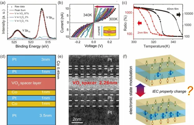
vacuum at room temperature. A broad peak has been found in the X-ray diffraction (XRD) result, indicating their amorphous feature (see Supplementary Figure S1). X-ray photoelectron spectroscopy (XPS) measurement is applied to check the valence state of vanadium. As shown in Figure 1A, the proportion of VO2 reaches 97%, which demonstrates the relatively pure
composition. The I-V curves with increasing temperature of a vertical tunnel junction device fabricated based on Au/VO2 (2 nm)/Au heterostructure are shown in Figure 1B, from which an
evolution from a tunneling contact to a transparent contact can be detected. The results indicate the dramatic change of the electronic property (i.e., an insulator to metal transition) in the VO2
spacer when the thermally triggered phase change occurs. Similar transport measurements of tunnel junctions with varied VO2 thickness can be found in Figure S2. Figure 1C presents the
ratio of the resistance change (calculated as the resistance divided by its minimum value) versus temperature with a measured current of 10 nA for a 2-nm-thick sample and a 40-nm-thick single-crystal film sample. It is noteworthy that the metal-insulator transition in the atomically-thin VO2
layer occurs at a temperature much lower than that of the bulk sample. This difference is probably caused by the effect of interfacial strain, interfacial bonds or defects25. Although
potential factors such as the amorphous nature and inevitable defects still affect the resistance change amplitude (~20 times), the hysteresis phenomenon proves the existence of the metal-insulator transition in the atomically-thin film.
The appreciable metal-insulator transition, good compatibility of the substrates and high vacuum room-temperature deposition conditions of the atomically-thin VO2 film further enable the
fabrication of VO2-based magnetic heterostructures. To investigate the effect of
spinterface-tailored IEC, we prepare a series of [Pt/Co]2/VO2/[Co/Pt]2 heterostructures (see Figure 1D for a
schematic diagram). VO2 layers with different thickness are adopted as the spacers, and Co/Pt
systems are chosen as the FM layers with PMA. Distinct interfaces between multilayers are verified by high-resolution transmission electron microscopy (HRTEM, see Figure 1E), by which the thicknesses of the atomically-thin VO2 spacers are calibratedto be 0.76, 1.48, 1.83 and 2.26
nm (see Figure S3). Some regions with microcrystalline morphology can also be observed within the VO2 layer, which may be caused by the fluctuations of the sputtering energy and
non-annealing process. These inevitable defects can explain the sluggish metal-insulator transition curve and non-uniform phase change process mentioned in the following discussion. In the VO2
-based magnetic heterostructures, the magnetic electrons in the top and bottom layers are coupled indirectly through atomically-thin VO2, whose electron density of 3d orbitals varies
tremendously during the metal-insulator transition. Considering the process of electron reflections between the two electrodes in the spacer, this variation not only influences the transport efficiency which alters the magnitude of the electron wave, but also changes the phase shift during the reflecting. As a result, the quantum well states of the system will be altered, which determines the energy favorable coupling state23. An unrevealed evolution of the IEC can thus
be expected owing tothe dramatic change in the VO2 spinterface (Figure 1F).
Electronic state induced IEC regulation
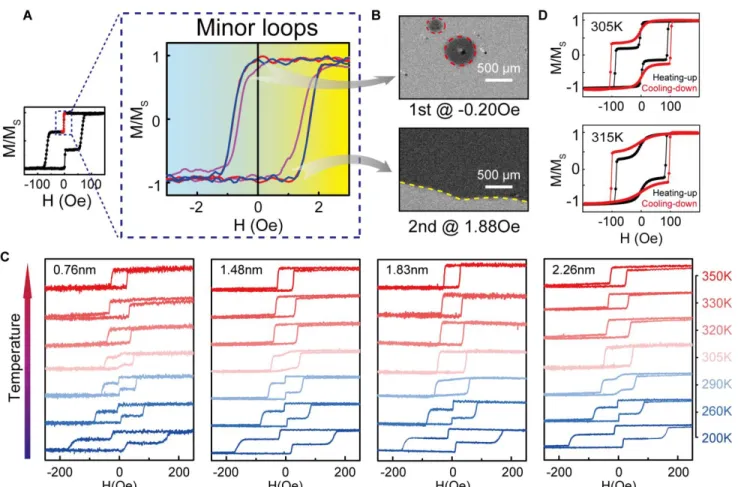
The IEC regulation in the phase change magnetic heterostructures is firstly investigated by magnetic property measurements. A vibrating sample magnetometer (VSM) is used to characterize the [Pt/Co]2/VO2/[Co/Pt]2 samples. As shown in Figure 2A, strong anisotropy is
detected in the sample with a 0.76-nm-thick VO2 spacer. Similar PMA properties can be found in
all the other films (see Figure S4). The magnetization shows two reorientation processes depending on the magnetic field, which indicates strong FM coupling within both the top and bottom Co/Pt bilayers. Thus, these bilayers will be treated as two single FM units when investigating the spinterface-tailored IEC effect.
As illustrated in Figures 2B-2E, hysteresis loops are also measured by the polar magneto-optic Kerr microscope (p-MOKE) before and after the metal-insulator transition for samples with different thickness of VO2. Interestingly, the two magnetization flips merge into one after the VO2
spacer change to be conducting for the 0.76-, 1.48-, 1.83- and 2.26-nm-thick VO2 spacer
samples. The experimental results of the control samples (with the structure of [Pt/Co]2/VO2 and
VO2/[Co/Pt]2, Figure S5) show that the magnetization reorientation fields of the two Co/Pt
bilayers are always different during the metal-insulator transition. Additionally, the phase change magnetic heterostructure shows no indication of anisotropy change, as the in-plane hysteresis loops coincide with each other during the metal-insulator transition (Figure 2F and Figure S6). These features thus exclude the possibility that the regulation is caused by the differentiated PMA modulation effect on the top and bottom magnetic layers, and especially confirm the appearance of strong FM coupling between top and bottom Co/Pt bilayers when the atomically-thin VO2 spacer becomes metallic.
To further understand this IEC regulation via dynamic modulation of the electronic states in VO2
spacer, one key issue is to distinguish the coupling state of the [Pt/Co]2/VO2/[Co/Pt]2 samples
when VO2 is insulating. Taking the sample with 0.76-nm-thick VO2 as an example, a
high-accuracy VSM with a built-in Hall probe (detecting high-accuracy of 0.01 Oe) is applied to collect the minor loop of the top magnetic layer. As shown in Figure 3A, a positive exchange bias Hex-top
(~0.35 Oe) can be detected in multiple measurements at room temperature. Further result shows that the value increases to 0.64 Oe when temperature is decreased to 200K, indicating the
existence of an AFM coupling through insulating VO2. To further confirm this result, the magnetic
domain switching behavior around the field region of the minor loop is also investigated, as shown in Figure 3B. The results verify that the domain switching of the top magnetic layer happens near -0.2 Oe and 1.88 Oe, also giving a positive value of Hex-top. Meanwhile, similar
minor loop measurements are carried out for other samples (see Figure S7), which suggest that the samples with 1.48-, 1.83-, and 2.26-nm-thick VO2 also exhibit AFM coupling for insulating
VO2 (Hex-top=0.57, 0.56 and 0.59 Oe, respectively). However, when the thickness of VO2 spacer
is greater than 3 nm, the sample exhibits a decoupling feature (Hex-top≈0.00 Oe), which meets
the fast decay feature of IEC. The dipolar effect, caused by the stray field of FM layers around the rough interfaces, can also result in ‘fake’ coupling. However, the HRTEM evidence of perfectly smooth interfaces (see Supplementary Figure S3E) indicates neglectable influence of this effect.
To obtain more details about the regulation effect, we then focus on the evolution of the IEC during the dynamic metal-insulator transition of VO2 triggered by temperature control. Figure 3C
shows the hysteresis loops of the samples at different temperatures. In all the four samples, there are double flips in the loops with insulating VO2. As the electronic property changing from
insulator to metal occurs, the loops feature a smooth flip of the top FM layer before a sudden transition into one single flip (that is, strong FM coupling). Interestingly, the critical temperature of the change in the IEC type shows a clear dependence on the VO2 thickness. For the two
thicker samples (1.83 nm and 2.26 nm), the FM coupling change occurs at a slightly lower temperature (approximately 310 K). Considering the similar deposition parameters of all samples, one possible reason for this difference is the appreciable interfacial strain effect on the metal-insulator transition temperature of the atomically-thin VO225. Considering that the VO2 exhibits
obvious hysteresis of metal-insulator transition (Figure 1C), the electronic state induced IEC regulation should exhibit the same feature. Therefore, we measure the magnetic loops of the 0.76-nm-thick VO2 sample at two temperatures within the hysteresis range (305 and 315 K)
during insulator to metal and metal to insulator transition processes (i.e., heating-up and cooling-down). As shown in Figure 3D, the sharpness of the flip in both results shows a clear difference, which proves our speculation and further verifies the origin of the IEC regulation as the metal-insulator transition of VO2. Further measurements (see Figure S8) indicate the excellent
repeatability of the AFM-to-FM coupling transition in these samples.
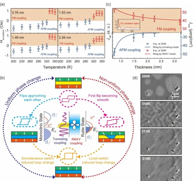
Based on the results obtained from all VO2-based magnetic heterostructures, the exchange bias
between two FM layers can be derived from the center shift of minor loops (for example the H ex-top in Figure 3A) or the shift of the flip edges relative to those of control samples31. Considering
the canted shape of the minor loops at high temperatures, we use the difference between the flip edge of the bottom FM layer (Figure 3C) and the coercive field of VO2/[Co/Pt]2 control sample
(Figure S9) to calculate the value of exchange bias field Hex-bottom. There are also some reports
about the presence of AFM ordering with insulating VO232. The calculation rule can thus eliminate
ex-bottom values represent AFM coupling, and the positive represent FM coupling. Samples with
various thickness of VO2 (0.76, 1.48, 1.83 and 2.26 nm) all demonstrate a transition from
appreciable AFM coupling through insulating VO2 spinterface to stronger FM coupling through
metallic VO2 spinterface.
Physical origin of the electronic state induced IEC regulation
Considering the complexity of the spinterface, the mechanism behind the regulation can be a combined result of various effects, including the variation in electronic state, interfacial strain, Co-O bonds and interface defects etc. during the phase change. However, as the VO2 layer is
amorphous, it is hard to form a uniform strain to have a long-range effect on the exchange coupling. For Co-O bonds or interface defects, the affected atoms are usually confined around the interface limited in a few angstroms,33,34 which is far thinner than the Co/Pt bilayer thickness.
Additionally, the magnetic anisotropy which is sensitive to these influences remains unchanged in the regulation process (Figure 2F), which indicates that they are not the major determinants. Since the IEC change shows a high correlation with phase change of VO2 (Figure 3C & 3D), it
is more convincing to attribute such a reversible coupling change to electronic state modulations of VO2.
To understand the possible mechanism, the phase change of VO2 should be taken into
consideration. As pointed out by Goodenough, the Peierl-like phase change of VO2 can produce
eliminate the band gap32,35. The distinct electronic states of VO2 can thus cause different IEC
origins and behaviors.To clarify the physical mechanism of IEC through insulating and metallic VO2 spinterface, the dependence of the coupling strength on VO2 thickness at 200 and 360 K is
shown in Figure 4B. The experimental values of coupling strength Jexp are determined from the
exchange bias field Hex-bottom using the relation 31,
exp= exbottom S1 1 S2 2 S1 1 S2 2
J H M t M t M t M t
, (Equation 1)
where t1 (0.9 nm) and t2 (2 nm) represent the thicknesses of Co layers in the top and bottom
magnetic layers, respectively, and MS1 and MS2 are their saturation magnetizations.
For IEC via insulating VO2 spinterface, the rapid decay of the coupling strength with thicker
spacer is consistent with the trend observed in oxide–based synthetic antiferromagnets21.
Considering the tunneling feature in the transport measurement of Au/VO2/Au junctions (Figure
1B & Figure S2), spin dependent tunneling, as suggested for the Co/MgO/Co system36, which
also features an exponential coupling strength decay, should dominate IEC in this case. The coupling strength then can be calculated as22:
3 2 2 2 2 2 2 2 2 2 2 2 8 ( )( ) ( ) ( ) 8 ( ) ( ) kd F cal k k k k k k k k U E J e d k k k k , (Equation 2)
Where Jcal is the calculated coupling strength, (U-EF) gives the barrier height of the
heterostructure, k↑, k↓ is the Fermi wave vectors for the spin up and down bands of the FM layers,
d is the thickness of the insulating spacer, and k is the wave vectors of electrons in the insulating
2 eff 2
2m (U EF)
k
, (Equation 3)
A barrier height value of 1 eV, referring to the work function of VO2 and Co37, and an effective
electron mass meff=1 me38, are adopted to perform the fitting of Jcal in Figure 4B, which perfectly
coincides with the experimental results of IEC through insulating VO2 (at 200 K). Notably, the
coupling strength shows a comparable value at AFM state to that of the FM state. According to previous research39, localized states within the band gap induced by defects can enhance the
coupling by spin dependent tunneling, and feature a strength decrease with temperature rising. Such an interpretation is consistent with the amorphous feature of the atomically-thin VO2 films
(Figure 1E) and the temperature dependence of the exchange field at AFM state (Figure 4A).
For the FM coupling via metallic VO2 spinterface, the most widely accepted coupling mechanism
is RKKY interaction. The coupling strength then can be calculated as40:
2 2 9 ( ) 64 cal F F J E , (Equation 4)
where δ is the coupling constant, υ is the number of conduction electrons per atom, EF is the
Fermi energy and F(ξ) is the RKKY function40 4
( ) (sin
cos ) /
F
, (Equation 5)where ξ=2kFd. The Fermi wavevector of free electrons kF is fitted to be 1.4*107 m-1 in the case
of metallic VO2 at 350 K. It appears clearly in Figure 4B that the experimental variation of the
coupling strength with the metallic VO2 spacer is well fitted with the framework of the RKKY
feature of an extremely large oscillation period (up to hundreds of nanometers, see Inset of
Figure 4B). As an example, an FM coupling of 37 μerg/cm3 can still be detected through a
metallic VO2 when its thickness reaches 3.22 nm. However, the coupling of this sample with
insulating VO2 is almost undetectable.
Besides the AFM to FM transition, the IEC evolution in our results accompanied by the smoothing of the first magnetization flip is different from a mere flip approaching behavior in a uniform IEC change route (Figure 4C). It can be explained by the inhomogeneous feature of the amorphous atomically-thin VO2 film41, which could induce domains with different conductivity and thus
non-uniform coupling during the metal-insulator transition. This speculation is confirmed by the Kerr microscope of the domain at critical switching state during the insulator to metal transition, which first evolves into a maze morphology, then finely breaks into smaller size beyond the resolution of the microscope (Figure 4D). With the in-plane loop measurement excluding the possibility of an anisotropy change (Figure 2F and Figure S6), it is reasonable to believe that this change is caused by the non-uniform phase change of VO2 providing more nucleation points for spin
switching.
Discussion
Overall, the IEC regulation in this work has been verified to get tailored by the electronic state of the VO2 spinterface. Compared to the modulation based on strain42 or ion migration14,15, such a
high speed (if with photonic excitation strategy43) and all-solid structure. Such a VO2 based
spinterface, with appreciable metal-insulator transition that can be induced by methods such as thermal heating25, electrical gating25, and especially pulse laser excitation43, would be a magic
building block for spinterface-tailored physical effects and device applications. As the spinterface plays an important role in abundant physical processes, in addition to IEC, it is reasonable to believe that such a modulation method can be used to control other spin electronic structures or magnetic materials, such as skyrmion, 2D ferromagnets and ferromagnetic insulators. After proving the close relationship between IEC and interlayer electronic state by this work, further realization of phase change by electrical methods will give birth to even richer applications in spintronics.
Conclusion
In conclusion, atomically-thin VO2 has been adopted as a spinterface with dramatically
changeable electronic properties to regulate the interlayer exchange coupling effect. Both the coupling strength and the type (that is, antiferromagnetic and ferromagnetic coupling) of the magnetic heterostructures [Pt/Co]2/VO2/[Co/Pt]2 can be tailored reversibly and repeatably
through the metal-insulator transition of VO2. Further analyses indicate that such an evolution
originates from two distinct physical mechanisms of spin dependent tunneling and RKKY interaction determined by the electronic states of VO2. As a proof-of-concept demonstration of
interface-tailored spintronics, this work might provide a general strategy for beyond-CMOS electronics.
Experimental Procedures
Resource Availability:
Lead Contact: Further information and requests for resources and reagents should be directed to and will be fulfilled by the Lead Contact, Weisheng Zhao ([email protected]). Materials Availability: This study did not generate new unique reagents.
Data and Code Availability: Data supporting the findings of this manuscript are available from the corresponding authors upon reasonable request. A reporting summary for this article is available as a Supplemental Information file.
Film deposition and device fabrication : The Au/VO2/Au and [Pt/Co]2/VO2/[Co/Pt]2
heterostructures were both grown on SiO2/Si substrates by magnetron sputtering at room
temperature under high vacuum. A stoichiometric target was used to deposit the VO2 film during
the experiments. The tunnel junctions were patterned by optical lithography (Micro Writer ML Baby, Durham Magneto Optics) followed by argon ion-beam etching of the bottom electrodes and pillars. Then, the samples were fully covered with SiO2 for insulation. After etching, a series
of vias were produced over the pillars to ensure the connection between the junction and the top electrodes. Both the bottom electrodes and tunnel junctions were then connected to 90-nm Ti/Au electrodes using e-beam evaporation to allow electrical contact for the measurements.
Characterization and measurement:The magnetic properties were measured by the MOKE
(NanoMOKE3, Durham Magneto optics ltd) with a homemade heat source and a VSM (7400, Lakeshore) at different temperatures. The Au/VO2/Au tunnel junctions were measured by normal
4-terminal methods with Keithley 6221 and Keithley 2182 source and measurements units, respectively. HRTEM was performed by a Talos F200X instrument. The XPS results were obtained by a Thermo Fisher ESCALAB 250Xi instrument, and the XRD measurements were performed by a Delta-X instrument.
Acknowledgments
We thank Prof. Albert Fert & Prof. Dapeng Zhu for helpful discussions. This work was supported by the National Natural Science Foundation of China (No. 51602013, 11804016, and 61627813), Young Elite Scientists Sponsorship Program by China Association for Science and Technology (CAST) (No. 2018QNRC001), the International Collaboration 111 Project (No. B16001), the Fundamental Research Funds for the Central Universities of China, and the Beijing Advanced Innovation Centre for Big Data and Brain Computing (BDBC), the French PIA project Lorraine Université d'Excellence, reference ANR-15-IDEX-0004, ICEEL and by Feder EU.
Author contributions
Conceptualization, X.Y.L. and W.S.Z.; Methodology, X.Y.L. and S. M.; Investigation, G.D.W. X.F.F., X.H.W., Z.Z.S., X.Y.Z. and X.Y.L.; Writing – Original Draft, G.D.W. X.F.F. and X.Y.L.; Writing – Review & Editing, G.D.W., X.Y.L., Q. S., S. M., E. F. and W.S.Z.; Resources, X.Y.L.,
W.S.Z., and L. J.; Funding Acquisition, X.Y.L., G.D.W., and W.S.Z.; Supervision, X.Y.L., and W.S.Z.
Declaration of Interests: The authors declare no competing interests.
References and Notes
1. Bader, S.D., and Parkin, S.S.P. (2010). Spintronics. Annu. Rev. Condens. Matter Phys. 1,
71–88.
2. Hellman, F., Hoffmann, A., Tserkovnyak, Y., Beach, G.S.D., Fullerton, E.E., Leighton, C.,
MacDonald, A.H., Ralph, D.C., Arena, D.A., Dürr, H.A., et al. (2017). Interface-induced
phenomena in magnetism. Rev. Mod. Phys. 89, 025006.
3. Lin, X., Yang, W., Wang, K.L., and Zhao, W. (2019). Two-dimensional spintronics for
low-power electronics. Nat. Electron. 2, 274–283.
4. De Teresa, J.M., Barthélémy, A., Fert, A., Contour, J.P., Montaigne, F., and Seneor, P.
(1999). Role of Metal-Oxide Interface in Determining the Spin Polarization of Magnetic
Tunnel Junctions. Science 286, 507–509.
5. Parkin, S.S.P., Kaiser, C., Panchula, A., Rice, P.M., Hughes, B., Samant, M., and Yang,
S.-H. (2004). Giant tunnelling magnetoresistance at room temperature with MgO (100)
tunnel barriers. Nat. Mater. 3, 862–867.
6. Kurnosikov, O., de Jong, J.E.A., Swagten, H.J.M., and de Jonge, W.J.M. (2002). Direct
80, 1076–1078.
7. Sato, N., Xue, F., White, R.M., Bi, C., and Wang, S.X. (2018). Two-terminal spin–orbit torque magnetoresistive random access memory. Nat. Electron. 1, 508–511.
8. Xie, Q., Lin, W., Yang, B., Shu, X., Chen, S., Liu, L., Yu, X., Breese, M.B.H., Zhou, T.,
Yang, M., et al. (2019). Giant Enhancements of Perpendicular Magnetic Anisotropy and
Spin-Orbit Torque by a MoS2 Layer. Adv. Mater. 31, 1900776.
9. Soumyanarayanan, A., Reyren, N., Fert, A., and Panagopoulos, C. (2016). Emergent
phenomena induced by spin–orbit coupling at surfaces and interfaces. Nature 539, 509– 517.
10. Wang, M., Cai, W., Zhu, D., Wang, Z., Kan, J., Zhao, Z., Cao, K., Wang, Z., Zhang, Y.,
Zhang, T., et al. (2018). Field-free switching of a perpendicular magnetic tunnel junction
through the interplay of spin–orbit and spin-transfer torques. Nat. Electron. 1, 582–588. 11. Yang, H., Chen, G., Cotta, A.A.C., N’Diaye, A.T., Nikolaev, S.A., Soares, E.A., Macedo,
W.A.A., Liu, K., Schmid, A.K., Fert, A., et al. (2018). Significant Dzyaloshinskii–Moriya interaction at graphene–ferromagnet interfaces due to the Rashba effect. Nat. Mater. 17, 605–609.
12. Fernández-Pacheco, A., Vedmedenko, E., Ummelen, F., Mansell, R., Petit, D., and
Cowburn, R.P. (2019). Symmetry-breaking interlayer Dzyaloshinskii–Moriya interactions in synthetic antiferromagnets. Nat. Mater. 18, 679–684.
13. Han, D.-S., Lee, K., Hanke, J.-P., Mokrousov, Y., Kim, K.-W., Yoo, W., van Hees, Y.L.W.,
in synthetic antiferromagnets. Nat. Mater. 18, 703–708.
14. Yang, Q., Wang, L., Zhou, Z., Wang, L., Zhang, Y., Zhao, S., Dong, G., Cheng, Y., Min,
T., Hu, Z., et al. (2018). Ionic liquid gating control of RKKY interaction in FeCoB/Ru/FeCoB
and (Pt/Co)2/Ru/(Co/Pt)2 multilayers. Nat. Commun. 9, 991.
15. Newhouse-Illige, T., Liu, Y., Xu, M., Reifsnyder Hickey, D., Kundu, A., Almasi, H., Bi, C.,
Wang, X., Freeland, J.W., Keavney, D.J., et al. (2017). Voltage-controlled interlayer
coupling in perpendicularly magnetized magnetic tunnel junctions. Nat. Commun. 8, 15232.
16. Liu, P., Lin, X., Xu, Y., Zhang, B., Si, Z., Cao, K., Wei, J., and Zhao, W. (2017). Optically
tunable magnetoresistance effect: From mechanism to novel device application. Materials.
11, 47.
17. Parkin, S.S.P., More, N., and Roche, K.P. (1990). Oscillations in exchange coupling and
magnetoresistance in metallic superlattice structures: Co/Ru, Co/Cr, and Fe/Cr. Phys. Rev.
Lett. 64, 2304–2307.
18. Ruderman, M.A., and Kittel, C. (1954). Indirect Exchange Coupling of Nuclear Magnetic
Moments by Conduction Electrons. Phys. Rev. 96, 99–102.
19. Inomata, K., Yusu, K., and Saito, Y. (1995). Magnetoresistance Associated with
Antiferromagnetic Interlayer Coupling Spaced by a Semiconductor in Fe/Si Multilayers.
Phys. Rev. Lett. 74, 1863–1866.
20. Gareev, R.R., Bürgler, D.E., Buchmeier, M., Olligs, D., Schreiber, R., and Grünberg, P.
(2001). Metallic-Type Oscillatory Interlayer Exchange Coupling across an Epitaxial FeSi
21. Chen, B., Xu, H., Ma, C., Mattauch, S., Lan, D., Jin, F., Guo, Z., Wan, S., Chen, P., Gao,
G., et al. (2017). All-oxide–based synthetic antiferromagnets exhibiting layer-resolved magnetization reversal. Science 357, 191–194.
22. Faure-Vincent, J., Tiusan, C., Bellouard, C., Popova, E., Hehn, M., Montaigne, F., and
Schuhl, A. (2002). Interlayer Magnetic Coupling Interactions of Two Ferromagnetic Layers
by Spin Polarized Tunneling. Phys. Rev. Lett. 89, 107206.
23. Bruno, P. (1995). Theory of interlayer magnetic coupling. Phys. Rev. B 52, 411–439. 24. Nakano, M., Shibuya, K., Okuyama, D., Hatano, T., Ono, S., Kawasaki, M., Iwasa, Y., and
Tokura, Y. (2012). Collective bulk carrier delocalization driven by electrostatic surface
charge accumulation. Nature 487, 459–462.
25. Liu, K., Lee, S., Yang, S., Delaire, O., and Wu, J. (2018). Recent progresses on physics
and applications of vanadium dioxide. Mater. Today 21, 875–896.
26. Wei, G., Lin, X., Si, Z., Lei, N., Chen, Y., Eimer, S., and Zhao, W. (2019).
Phase-transition-induced large magnetic anisotropy change in VO2/(Co/Pt)2 heterostructure. Appl. Phys.
Lett. 114, 012407.
27. Wei, G., Lin, X., Si, Z., Wang, D., Wang, X., Fan, X., Deng, K., Liu, K., Jiang, K., Lei, N.,
et al. (2020). Optically Induced Phase Change for Magnetoresistance Modulation. Adv.
Quantum Technol. 1900104, 1900104.
28. Fan, L.L., Chen, S., Wu, Y.F., Chen, F.H., Chu, W.S., Chen, X., Zou, C.W., and Wu, Z.Y.
(2013). Growth and phase transition characteristics of pure M-phase VO2 epitaxial film
29. Gupta, A., Narayan, J., and Dutta, T. (2010). Near bulk semiconductor to metal transition
in epitaxial VO2 thin films. Appl. Phys. Lett. 97, 151912.
30. Vernardou, D., Pemble, M.E., and Sheel, D.W. (2004). Vanadium oxides prepared by
liquid injection MOCVD using vanadyl acetylacetonate. Surf. Coatings Technol. 188–189, 250–254.
31. Nistor, L.E., Rodmacq, B., Auffret, S., Schuhl, A., Chshiev, M., and Dieny, B. (2010).
Oscillatory interlayer exchange coupling in MgO tunnel junctions with perpendicular
magnetic anisotropy. Phys. Rev. B 81, 220407.
32. Eyert, V. (2002). The metal-insulator transitions of VO2: A band theoretical approach. Ann.
Phys. 11, 650–704.
33. Oleinik, I.I., Tsymbal, E.Y., and Pettifor, D.G. (2002). Atomic and electronic structure of
Co/SrTiO3/Co magnetic tunnel junctions. Phys. Rev. B 65, 1–4.
34. Oleinik, I., Tsymbal, E.Y., and Pettifor, D. (2000). Structural and electronic properties of
magnetic tunnel junction from first principles. Phys. Rev. B 62, 3952–3959.
35. Goodenough, J.B. (1971). The two components of the crystallographic transition in VO2.
J. Solid State Chem. 3, 490–500.
36. Yuasa, S., Fukushima, A., Kubota, H., Suzuki, Y., and Ando, K. (2006). Giant tunneling
magnetoresistance up to 410% at room temperature in fully epitaxial Co/MgO/Co magnetic
tunnel junctions with bcc Co(001) electrodes. Appl. Phys. Lett. 89, 1–4.
37. Yin, H., Luo, M., Yu, K., Gao, Y., Huang, R., Zhang, Z., Zeng, M., Cao, C., and Zhu, Z.
VO2 Nanostructures. ACS Appl. Mater. Interfaces 3, 2057–2062.
38. Kang, M., Kim, S.W., and Ryu, J.-W. (2015). Analysis of diverging effective mass extracted
from thermoelectric power across the metal–insulator transition in VO2. J. Appl. Phys. 118,
035105.
39. Zhuravlev, M.Y., Tsymbal, E.Y., and Vedyayev, A. V. (2005). Impurity-Assisted Interlayer
Exchange Coupling across a Tunnel Barrier. Phys. Rev. Lett. 94, 026806.
40. Parkin, S.S.P., and Mauri, D. (1991). Spin engineering: Direct determination of the
Ruderman-Kittel-Kasuya-Yosida far-field range function in ruthenium. Phys. Rev. B 44,
7131–7134.
41. Kawatani, K., Takami, H., Kanki, T., and Tanaka, H. (2012). Metal-insulator transition with
multiple micro-scaled avalanches in VO2 thin film on TiO2 (001) substrates. Appl. Phys.
Lett. 100, 173112.
42. Wang, X., Yang, Q., Wang, L., Zhou, Z., Min, T., Liu, M., and Sun, N.X. (2018). E-field
Control of the RKKY Interaction in FeCoB/Ru/FeCoB/PMN-PT (011) Multiferroic
Heterostructures. Adv. Mater. 30, 1803612.
43. Morrison, V.R., Chatelain, R.P., Tiwari, K.L., Hendaoui, A., Bruhács, A., Chaker, M., and
Siwick, B.J. (2014). A photoinduced metal-like phase of monoclinic VO2 revealed by
Figures and Tables
Figure 1. Atomically-thin VO2 and magnetic heterostructures.
(A) X-ray photoelectron spectroscopy (XPS) profile of the sample with peak fitting results. The proportion of VO2 reaches 97%.
(B) I-V curve of the VO2 tunnel junction measured at different temperatures with the current
flowing vertically through the device. The insert gives the schematic of the device which is fabricated based on Au/VO2 (2 nm)/Au heterostructures with a diameter of 10 μm.
(C) The resistance change ratios versus temperature of 2-nm- and 40-nm-thick VO2 films with a
current of 10 nA, which indicate the existence of metal-insulator transition. The resistance change ratio is defined as the temperature dependent resistance divided by its minimum value. (D) The schematic of the [Pt/Co]2/VO2/[Co/Pt]2 heterostructures.
(E) High-resolution transmission electron microscopy (HRTEM) image of the [Pt/Co]2/VO2 (2.26
nm)/[Co/Pt]2 sample with distinct interfaces.
(F) Schematic diagram of the spinterface-tailored interlayer exchange coupling (IEC) effect. The insulator to metal transition of VO2 spinterface can enhance the electron density of 3d orbitals
Figure 2. Magnetic properties of [Pt/Co]2/VO2/[Co/Pt]2 heterostructures.
(A) Hysteresis loops of the [Pt/Co]2/VO2 (0.76 nm)/[Co/Pt]2 sample measured by vibrating
sample magnetometer (VSM) at room temperature with magnetic field applied in-plane (red line, step size 200Oe) and out-of-plane (blue line, step size 2 Oe), where M is the magnetization of the magnetic layers; Ms is the saturation magnetization, H is the external magnetic field.
(B)-(E) Hysteresis loops of the heterostructure samples measured by polar magneto-optic Kerr microscope (p-MOKE, measurement frequency 0.1 Hz) with VO2 at insulating state (IS, 300 K,
black line) and metallic state (MS, 360 K, red line), where the thickness of VO2 spacer is 0.76,
1.48, 1.83 and 2.26 nm, respectively. The two magnetization flips merge into one after the insulator to metal transition.
(F) In-plane hysteresis loops of the [Pt/Co]2/VO2 (0.76 nm)/[Co/Pt]2 sample at different
temperatures measured by VSM (step size 100 Oe), which show no indication of anisotropy change in the metal-insulator transition. The inset gives the enlarged image from -1000 to 1000 Oe.
Figure 3. Regulation of IEC during metal-insulator transition process.
(A) Minor loops of [Pt/Co]2/VO2 (0.76 nm)/[Co/Pt]2 sample obtained by VSM in the magnetic field
range of ±3 Oe with a step of 0.1 Oe.
(B) Magnetic domain switching behavior of the sample around the minor loop field range obtained from Kerr microscope with out-of-plane field applied. The center deviation of minor loop indicates the existence of an AFM coupling.
(C) The variation of hysteresis loops measured by VSM (step size 0.5 Oe) at different temperatures for [Pt/Co]2/VO2/[Co/Pt]2 samples with VO2 of 0.76, 1.48, 1.83, 2.26 nm
respectively. The loop features a smooth flip of the top FM layer before a sudden transition into one single flip, and the critical temperatures of IEC type change show obvious difference. (D) The comparison of the hysteresis loops during heating-up and cooling-down process at 305 K and 315 K. The sharpness of the flip in both results shows a clear difference which is consistent with VO2 hysteresis feature.
Figure 4. Mechanism of spinterface-tailored IEC via metal-insulator transition.
(A) Exchange bias field of bottom magnetic layer (Hex-bottom) versus temperature for 0.76, 1.48,
1.83 and 2.26 nm VO2, respectively.
(B) Thickness dependence of coupling strength obtained from experiment (Jexp) and calculation
(Jcal) with insulating (at 200 K) and metallic (at 360 K) VO2 spinterface, respectively. The solid
blue line is a fitting curve according to the spin dependent tunneling theory with parameters of barrier height 1 eV, effective mass of meff=1me. The solid red line is a fitting curve following the
RKKY theory with kF=1.4*107 m-1. Right Y axis has been broken from -25 to 25 μerg/cm3. The
inset gives the IEC oscillation calculated from the RKKY model over broad range of VO2
thickness, which indicates the characteristics of an extremely large oscillation period (up to hundreds of nanometers).
(C) Schematic diagram of the IEC regulation mechanism. The inner image gives the energy band variation of VO2 and corresponding coupling mechanism before and after the insulator to
metal transition. The spectral weight transfer from π* (dxy) orbitals into the valence d// (dxz, yz)
orbitals enhances the electron density near Fermi surface, and makes coupling mechanism change from the spin dependent tunneling to RKKY interaction. The outside gives the different
spin dynamic evolution process with uniform (left arrow) and non-uniform (right arrow) phase change. For the non-uniform phase change, the electric domain in VO2 may induce local
magnetic domain switching during the metal-insulator transition.
(D) The magnetic domain morphology of 0.76-nm-thick VO2 film observed by Kerr microscope
![Figure 2. Magnetic properties of [Pt/Co] 2 /VO 2 /[Co/Pt] 2 heterostructures.](https://thumb-eu.123doks.com/thumbv2/123doknet/14439528.516657/26.918.93.833.113.490/figure-magnetic-properties-pt-vo-pt-heterostructures.webp)