Composition, Structure, and Performance of Nanocrystal Bulk Heterojunction Photovoltaics
by MASSACHUSETTS INSTITUTE
OF TECHNOLOLGY
Kevin J. Huang JUN 172015
B.S., Cornell University (2006)
M.S., University of Illinois, Urbana-Champaign (2007)
LIBRARIES
Submitted to the Department of Materials Science and Engineering in Partial Fulfillment of the Requirements for the Degree of
Doctor of Philosophy at the
MASSACHUSETTS INSTITUTE OF TECHNOLOGY
June 2015
0 2015 Massachusetts Institute of Technology. All rights reserved.
Signature
redacted
Signature of A uthor ... . ... ... ... ...
Department of laterials S Aence Engineering
/I F ruary 12, 2015
Certified by ...
Signature redacted
...
Paula Hammond David H. Koch Professor in Engineering Thesis SupervisorSianature redacted
Accepted by...
... ...
Angela Belcher Professor olo jalngineering and Materials Science and Engineering Thesis Reader
Signature
redacted
...
Donald R. Sadoway Chair Departmental Committee on Graduate Students A cc e t bk
Composition, Structure, and Performance of Nanocrystal Bulk Heterojunction Photovoltaics
by
Kevin J. Huang
Submitted to the Department of Materials Science and Engineering on February 12, 2015 in partial fulfillment of the requirements for the degree of Doctor of Philosophy in Materials
Science and Engineering
ABSTRACT
We describe the fabrication and study of bulk heterojunction solar cells composed of PbS quantum dots and TiO2. In particular, we study the effects that bulk heterojunction composition
and structure have on resulting device performance.
We find that PbS and titania are extremely evenly distributed throughout our bulk heterojunction devices, such that charge carriers generated anywhere within the blend are well within a carrier collection length of the charge separating driving force required to separate them and enable their collection. Of the compositions we studied, we found that devices with a TiO2
-rich bulk heterojunction composition outperformed devices employing other compositions. As a result of the size difference between the PbS quantum dots and the titania nanocrystals which compose the blends, the likelihood of forming a truly complete, bicontinuous bulk heterojunction network is maximized at a TiO2-rich blend composition.
We find that diffuse interfaces exist between adjacent layers of our devices as a result of interfacial surface roughness. Rather than being deleterious, this increased interfacial area extends the spatial extent of the depletion region over a greater volume of our devices. Our bulk heterojunction blends form well packed, high density binary particle mixtures, particularly at a TiO2-rich composition. Device efficiency was maximized for bulk heterojunctions employing
the smallest titania nanocrystals, an indication that at constant volume fractions, larger titania nanocrystals decrease the total number of titania particles available to form complete and continuous pathways through the depth of the bulk heterojunction. Furthermore, a peak in device performance was observed at intermediate blend layer thicknesses. This results from the balance between two opposing effects: an increase in light absorption and photocurrent with thicker bulk heterojunctions and an increased likelihood of charge carrier recombination with thicker bulk heterojunctions.
Finally, enhanced light absorption and current generation was observed at red and infrared wavelengths, validating the ability of bulk heterojunctions to spatially extend the reach of the charge separating driving force, such that the previously missed red and infrared photons may be captured.
Thesis Supervisor: Paula Hammond
Acknowledgments
First and foremost, I would like to thank my friends and family for all the support, in every conceivable way, they've given me over my thirty-one years.
Second, I'd like to thank my thesis advisors, Professor Paula Hammond and Professor Angela Belcher. Their patience and support throughout my time as a graduate student has been remarkable, always constant, and exceedingly high.
Third, I'd like to thank my peers in the Hammond and Belcher groups for all their invaluable help. In particular, I'd like to single out Noemie-Manuelle Dorval Courchesne, Matthew Klug, and Po-Yen Chen. It is not an exaggeration to say that without their help, I would not have completed this work.
Fourth, I'd like to thank my thesis committee members, Professor Michael Strano and Professor Michael Rubner, for the time and thoughtfulness they put into overseeing my progress.
Fifth, I'd like to thank the staff at the various shared experimental facilities throughout MIT that enabled me to complete my work. This includes the Center for Materials Science and Engineering, the Institute for Solider Nanotechnologies, and the Organic and Nanostructured Electronics Lab.
And last, I'd like to thank the various sources of financial support that provided for my work at MIT. This includes the NSF Graduate Research Fellowship, the National Defense Science and Engineering Graduate Fellowship, funding from the MIT Energy Initiative, and funding from Eni
Table of Contents
Chapter 1: Introduction and Motivation 8
Why Solar Energy 12
Fundamentals of Quantum Dot Photovoltaics 23
Improvements to Quantum Dots 26
Improvements in Charge Extraction 30
Measuring Photovoltaic Device Performance 41
Looking Ahead 43
Chapter 2: PbS and TiO2 Nanocrystals 47
Synthesis and Characterization of PbS Quantum Dots 47
Materials 47
Methods 48
Quantum Dot Structure 50
Quantum Dot Passivation 55
Synthesis and Characterization of TiO2 Nanocrystals 60
Materials 60
Methods 60
Nanocrystal Structure 61
Nanocrystal Ligands 71
Chapter 3: Effect of Composition on Nanocrystal Bulk Heterjunction Photovoltaics 73
Materials and Methods 73
Device Composition 76
Device Performance 85
Origin of Device Performance 86
Chapter 4: Effect of Structure on Nanocrystal Bulk Heterojunction Photovoltaics 97
Materials and Methods 98
Device Structure 100
Effect of TiO2 Nanocrystal Size 108
Effect of Blend Layer Thickness 117
Chapter 5: Conclusions and Outlook 126
Table of Figures
Figure 1. Example of some, but not all, likely human impacts of climate change [10]... 11
Figure 2. Global annual resource potential for various renewable energy technologies compared with
global annual primary energy use and annual electricity use in 2010 [16-20]. ... 13
Figure 3. Solar resource potential for the United States [23]... 14
Figure 4. Solar photovoltaic resource potential for the United States, Spain, and Germany [24]... 15 Figure 5. Various CSP technologies. (a) parabolic trough, (b) dish Stirling engine, (c) solar power tower
[2 6 -2 8 ]. ... 1 7
Figure 6. Certified record power conversion efficiencies for various types of photovoltaic cells over time
[3 3 ]...2 0 Figure 7. Photovoltaic technology roadmap plotting various generations of solar cell technology by their efficiency and manufacturing cost. Also indicated are various efficiency limits and important module co st th resh o ld s [3 4 ]...2 1 Figure 8. Levelized cost of electricity for utility scale photovoltaic power plants [35]...22 Figure 9. (a) AMI.5G solar spectrum with the bandgaps for various bulk semiconductors indicated. (b)
Solar spectrum with various quantum dot size-dependent energy gaps indicated [38]. ... 24
Figure 10. Schematic illustration comparing the molecules (and their respective sizes) involved in the traditional organic ligand passivation as well as the newly developed atomic ligand passivation scheme
[5 2 ]...2 9
Figure 11. Schematic energy band diagram of a Schottky junction solar cell comprised of PbS quantum
dots. Ec = conduction band, Ev = valence band, Evac= vacuum energy level, EF= Fermi level, Eg
b an d g ap [5 5 ]. ... 3 1
Figure 12. Schematic energy band diagram of a depleted heterojunction illustrating the charge-separating
depletion region centered at the heterojunction interface [60]... 32
Figure 13. Computer simulated images of bulk heterojunction blends from an organic bulk heterojunction d ev ic e [6 5 ]. ... 3 4 Figure 14. Examples of bulk heterojunction structures used in PbS quantum dot based solar cells. (a) disordered bulk heterojunction in which the QDs are infiltrated into a porous nanoparticle film, (b) ordered bulk heterojunction in which QDs are infiltrated into vertically aligned nanowires, (c) disordered bulk heterojunction in which two sulfide QDs are blended together and cast into a film [60]...35
Figure 15. (a, c) Schematic illustration of a bilayer heterojunction of PbS and Bi2S3 nanocrystals and its
accompanying cross sectional scanning electron micrograph, (b, d) schematic illustration of a bulk
heterojunction of PbS and Bi2S3 nanocrystals and its accompanying cross sectional scanning electron
m icro grap h [7 1]. ... 3 8
Figure 16. Schematic illustration of how the spatial extent of the depletion region in PbS (in grey and indicated by d) can be tuned by altering the work function of the underlying electrode, resulting in a
significant leap forward to a new record device efficiency [73]... 40
Figure 17. Schematic illustration of a model J-V curve from an illuminated solar cell [38]...42 Figure 18. Cross sectional scanning electron micrograph of PbS QDs infiltrated into ZnO nanowires,
indicating several large scale voids where incomplete infiltration has occurred [62]. ... 45
Figure 19. TEM micrographs of as-synthesized PbS quantum dots. ... 51
Figure 20. Powder X-ray diffractogram of as-synthesized PbS quantum dots. ... 52
Figure 21. UV-vis absorption spectra of PbS quantum dots synthesized at different reaction temperatures.
... 5 4
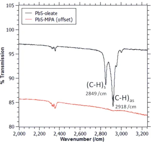
Figure 22. FTIR spectra of PbS quantum dots capped in oleate (as-synthesized) and capped with
3-mercaptopropionic acid (ligand exchanged during device fabrication)... 57
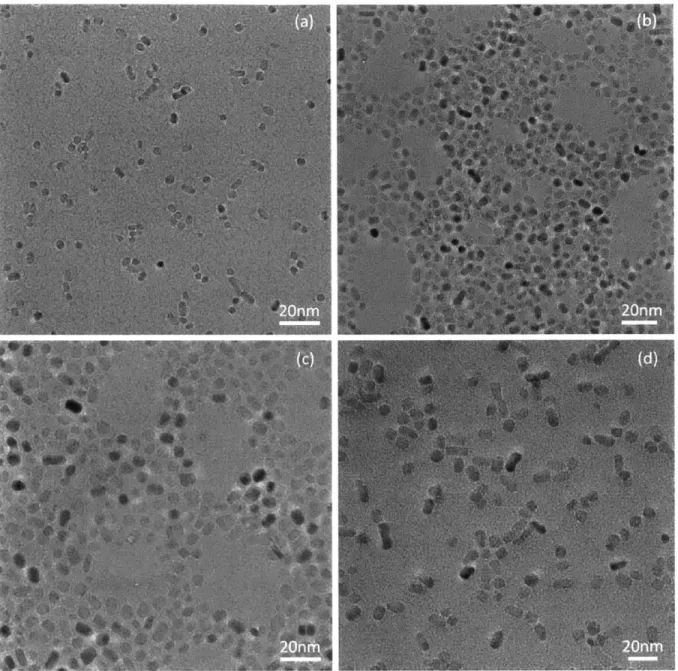
Figure 24. TEM micrographs for titania nanocrystals synthesized for 8hr at (a) 175'C, (b) 200'C, (c)
22 50C , an d (d ) 2 50 C ... 6 3
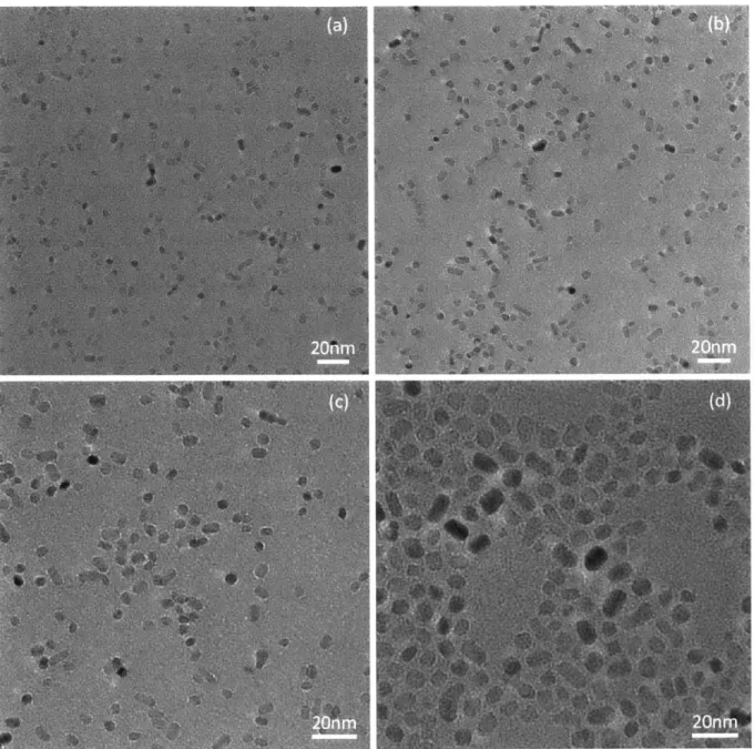
Figure 25. TEM micrographs for titania nanocrystals synthesized at 175'C for (a) 8hr, (b) 12hr, (c) 16hr,
an d (d ) 2 0 h r...6 5
Figure 26. Size histograms for titania nanocrystals synthesized at (a) 175'C for 8 hours, (b) 200'C for 8
hours, (c) 225'C for 8 hours, (d) 250'C for 8 hours, (e) 1750C for 12 hours, (f) 175'C for 16 hours, and
(g) 175'C for 20 hours. Quantile boxes for each histogram are also presented. The rectangle boxes
bound the standard deviation around the mean (indicated by the diamond) and the median (indicated by
the short vertical line in the m iddle of each box)... 67
Figure 27. Titania nanocrystal size vs. synthesis temperature (at an 8 hour reaction time) and time (at a reaction tem perature of 175'C )...68 Figure 28. XRD spectra of bulk crystalline anatase titania, amorphous titania, and our synthesized anatase titania nanocrystals...70 Figure 29. Evolution of titania nanocrystal structure over the reaction temperature and reaction time ran ge s stu d ied ... 7 1
Figure 30. FTIR spectra of as-synthesized titania nanocrystals with oleate (and, to a lesser extent, oleylamine) capping ligands compared with nanocrystals whose ligands have been exchanged for MPA.
... 7 2
Figure 31. Schematic illustrations of (a) bilayer heterojunction device of PbS QDs and titania base layer composed of either nanoparticle paste or anatase nanocrystals, and (b) bulk heterojunction device of PbS QDs, a blend layer of QDs and titania nanocrystals, and a titania base layer composed of either
nanoparticle paste or anatase nanocrystals. Blue = fluorine-doped tin oxide, Green = TiO2, Red = PbS,
G rey = M oO 3, Y ellow = A u. N ot to scale... 77
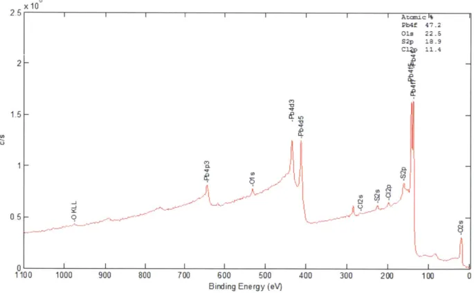
Figure 32. EDX surface maps of thin film blends of PbS quantum dots and titania nanocrystals from a bulk heterojunction device...78 Figure 33. Surface XPS survey of a bulk heterojunction blend layer of PbS quantum dots and titania
nanocrystals and a pure layer of PbS deposited over an underlying pure layer of titania. ... 80
Figure 34. XPS depth profile of a bilayer device in which PbS is deposited on top of an underlying titania p aste b ase lay er...82
Figure 35. XPS depth profiles of bulk heterojunction blend layers composed of varying ratios of PbS QDs and titania nanocrystals. (a) 25% volume fraction PbS, (b) 50% volume fraction PbS, (c) 75%
vo lum e fraction P b S ... 84
Figure 36. J-V curves for representative bulk heterojunction solar cells comparing devices with Pb-rich
blend layers (75% volume fraction PbS) and TiO2-rich blend layers (25% volume fraction PbS) for
devices with (a) titania nanocrystal base layers and (b) titania paste base layers...86 Figure 37. Averaged power conversion efficiency as a function of PbS volume fraction in the bulk heterojunction blend layer for devices employing (a) a titania nanocrystal base layer or (b) a titania paste b a se lay e r. ... 8 7
Figure 38. Averaged photocurrent as a function of PbS volume fraction in the bulk heteroj unction blend layer for devices employing (a) a titania nanocrystal base layer or (b) a titania paste base layer. ... 88 Figure 39. Averaged fill factor as a function of PbS volume fraction fraction in the bulk heterojunction blend layer for devices employing (a) a titania nanocrystal base layer or (b) a titania paste base layer...89 Figure 40. Averaged shunt resistance as a function of PbS volume fraction fraction in the bulk
heterojunction blend layer for devices employing (a) a titania nanocrystal base layer or (b) a titania paste b a se lay e r. ... 9 0
Figure 41. Averaged series resistance as a function of PbS volume fraction fraction in the bulk
heterojunction blend layer for devices employing (a) a titania nanocrystal base layer or (b) a titania paste b a se lay e r. ... 9 1
Figure 42. Averaged photovoltage as a function of PbS volume fraction in the bulk heterojunction blend layer for devices employing (a) a titania nanocrystal base layer or (b) a titania paste base layer. ... 92
Figure 43. Effect of particle size mismatch on bicontinuity threshold (expressed as film composition) in binary particle m ixtures [87]...93
Figure 44. EQE spectra for bulk heterojunction devices employing TiO2-rich blend layers (25% volume
fraction PbS) and PbS-rich blend layers (75% volume fraction PbS) for devices using (a) a titania
nanocrystal base layer or (b) a titania paste base layer ... 96
Figure 45. Cross sectional SEM micrograph of PbS QD layer on top of titania paste base layer. ... 102 Figure 46. Cross sectional SEM micrograph of PbS QD layer on top of a blend layer of PbS dots and
titania nanocrystals, with an underlying base layer of titania nanoparticle paste. ... 103
Figure 47. XPS depth profiles of PbS QDs deposited on top of (a) a titania nanocrystal base layer, and (b)
a blend layer of PbS dots and titania nanocrystals with 25% PbS volume fraction... 105
Figure 48. Effect of film composition on film packing density (at various particle size ratios) for binary
particle m ixtures (of m illim eter-scale particles) [82]... 107
Figure 49. J-V curves for representative bulk heterojunction solar cells comparing devices with large titania nanocrystals and small titania nanocrystals (6.92nm average size) for devices with (a) titania
nanocrystal base layers and (b) titania paste base layers. ... 109
Figure 50. Averaged power conversion efficiency as a function of titania nanocrystal size for bulk heteroj unction devices employing (a) a titania nanocrystal base layer or (b) a titania paste base layer... 110 Figure 51. Averaged short circuit current density as a function of titania nanocrystal size for bulk
heterojunction devices employing (a) a titania nanocrystal base layer or (b) a titania paste base layer... 111 Figure 52. Averaged fill factor as a function of titania nanocrystal size for bulk heterojunction devices
employing (a) a titania nanocrystal base layer or (b) a titania paste base layer... 112
Figure 53. Averaged shunt resistance as a function of titania nanocrystal size for bulk heterojunction devices employing (a) a titania nanocrystal base layer or (b) a titania paste base layer... 113 Figure 54. Averaged series resistance as a function of titania nanocrystal size for bulk heterojunction
devices employing (a) a titania nanocrystal base layer or (b) a titania paste base layer... 114
Figure 55. Averaged open circuit voltage as a function of titania nanocrystal size for bulk heterojunction devices employing (a) a titania nanocrystal base layer or (b) a titania paste base layer... 115 Figure 56. J-V curves for representative bulk heterojunction solar cells comparing devices with a bilayer architecture vs. a bulk heterojunction architecture for devices with (a) titania nanocrystal base layers and
(b) titania paste b ase layers... 117
Figure 57. Averaged power conversion efficiency as a function of blend layer thickness for bulk
heterojunction devices employing (a) a titania nanocrystal base layer or (b) a titania paste base layer... 118 Figure 58. Averaged short circuit current density as a function of blend layer thickness for bulk
heteroj unction devices employing (a) a titania nanocrystal base layer or (b) a titania paste base layer... 119 Figure 59. Averaged fill factor as a function of blend layer thickness for bulk heterojunction devices
employing (a) a titania nanocrystal base layer or (b) a titania paste base layer... 120
Figure 60. Averaged shunt resistance as a function of blend layer thickness for bulk heterojunction
devices employing (a) a titania nanocrystal base layer or (b) a titania paste base layer... 121
Figure 61. Averaged series resistance as a function of blend layer thickness for bulk heterojunction devices employing (a) a titania nanocrystal base layer or (b) a titania paste base layer... 122 Figure 62. Averaged open circuit voltage as a function of blend layer thickness for bulk heterojunction devices employing (a) a titania nanocrystal base layer or (b) a titania paste base layer... 123 Figure 63. EQE spectra comparing bilayer and bulk heterojunction device architectures for devices using
(a) a titania nanocrystal base layer or (b) a titania paste base layer... 125
Table 1. Summary of how PbS quantum dot reaction temperature affects ultimate dot size and its resulting optical properties...54
Chapter 1: Introduction and Motivation
Energy has been a part of human society ever since the very beginning. Global primary energy consumption in 2013 was 533 EJ, up from 27.4 EJ in 1850 [1, 2], an increase of over 1800%. During the same time period, the world's population grew by "only" 460% [3]. As can be seen
by the large disparity in growth rates, we as a society are consuming ever growing amounts of
energy per person. Accordingly, methods and technologies for capturing, converting, storing, distributing, and consuming energy will only continue to increase in importance to match our simultaneously and ever increasing thirst for energy.
Presently, however, the vast majority of our energy is supplied from sources that are non-renewable and finite. These resources are also not evenly distributed around the world. Moreover, it is clear that our reliance on carbon-based sources of energy is causing extremely rapid and increasingly irreversible large scale changes to our climate. These factors, among others, are driving interest toward the development of novel and sustainable ways of producing energy, whether it's out of fear that our resources will soon run out, fear that our domestic sources of energy will dwindle and make us politically and economically reliant on foreign nations (not necessarily of our own choosing), or fear that we are forever damaging our world in ways that will last for centuries to come and may not be reversible.
Energy is a massive industry. With the global market estimated at a size of $6 trillion, energy is the third largest industry in the United States [4]. Aside from the clear financial and economic opportunity to capitalize on emerging technologies and business models for such a large industry, there's also an undercurrent of national competition that often pervades the discussion around "American" or "domestic" energy. And in the race to maintain leadership in the global economy, and by extension global politics, leadership in energy is a promising pathway.
This sort of nationalistic rhetoric can be particularly acute when oil prices are high, as they were in the summer of 2008 when oil was priced at over $140 per barrel [5] given that much of our nation's oil is imported, often from nations mired by political instability. Beyond oil, the security of our national electric power transmission and distribution grids is also of concern. Blackouts can result in significant economic loss while there's evidence that our national infrastructure, such as the power grid, is susceptible to attack [6]. And recent events unfolding in the Ukraine have once again shine a spotlight on the Russian supply of natural gas to Europe and the associated supply and security concerns that accompany that dependent relationship. National security or national "competitiveness" remains a driving force behind the development of new domestic and sustainable energy solutions.
But perhaps the greatest concern that is motivating (or should be motivating) a transition to more sustainable sources of energy is climate change. At the start of the industrial revolution, the atmospheric CO2 concentration was approximately 280 ppm by volume. Largely as a result of
human reliance on carbon based sources of energy that emit excessive amounts of C02, a long lifetime greenhouse gas, atmospheric CO2 concentrations have already passed 400ppm. CO2 concentrations haven't been this high in at least 800,000 years, if not upwards of 15 million years
[7]. As a consequence of this, global mean surface temperatures continue to rise to unprecedented levels. With high confidence, this has and will continue to have numerous physical and environmental effects:
1. Dramatic increase in global average surface temperature
2. Decreased global snow and sea ice cover as well as decreased glaciation
3. Rising sea levels
5. Decreased ocean oxygenation
6. More extreme weather (dry and drought stricken regions will be more so, areas
vulnerable to high precipitation events will be even more affected by them)
7. Increased fire frequency and intensity in vulnerable areas
8. Destabilization of gas hydrate and permafrost-based methane deposits (i.e.,
further release of methane)
From these effects, it is not difficult to extrapolate the severe impacts this will have on ecosystems around the world as well as on human society, particularly on food security and supply [8], water availability, human health [9], human conflict, human conflict with other animal species, the built environment and man-made infrastructure, and human industry. Climate change is unique in that it remains a challenge that affects not just some parts of society (e.g., only some geographic regions, only some socio-economic classes, or only some ethnicities), but all of it. And as a consequence, its impacts are so far ranging that estimation, quantification, and projection of all of them remains an ongoing process. Figure 1 presents some, but certainly not all, likely impacts of climate change on human society. Far from being a widely divided, the majority of climate scientists believe that climate change is largely caused by humans, that it imposes significant risks, and that immediate efforts should be taken to curb the emissions of greenhouses gases into the atmosphere [10].
Table 3.2. Examples of possible impacts of clknate change due to changes in extreme weather and climate events, based on projections to the mid- to late 21' century These do not take into account any changes or developments in adapie capacity The likelihood esUmates in column two
relate to the ohenomena listed in column one. [WGl Table SPMI 11
Increased yields in colder environments; decreased yields in warmer environments; increased insect outbreaks Reduced yields In warmer regions due to heat stress; Increased danger of wildfire
Damage to crops; soil erosion, inability to cultivate land due to wateroggirig of soils
Land degradation;
lower ylields/crop damage and failure;
increased livestock deaths; increased risk of wildfire Damage to crops windthrow (uprooting) of trees; damage to coral reefs SalInisation of Irrigation water, estuaries and fresh-water systems
Effects on water Reduced human Reduced energy demand for resources relying on mortally from heating; increased demand unowmelt; effects on decreased cold for cooling; declining air quality some water supplies exposure in cities; reduced disruption to
transport due to snow, ice; effects on winter tourism increased water Increased risk of Reduction in quality of life for demand water heat-related people in warm areas without
qualty problems. mortaflty especially appropriate housing; Impacts
e.g. algal blooms for the sidedly. on the elderly, very young and chronically sick, poor
very young and
socially isolated Adverse effects on
quality of surface and groundwater; contamination of water supply; water scarcity may be relieved More widespread water stress Power outages causing disruption of public water supply
Decreased fresh-water availability due to saltwater Intrusion
Increased risk of
death&, Injuries and
Infiscuous, respwatory and skin diseases
Increased risk of food and water shortage; increased risk of malnutrition; Increased risk of water- and
food-borne diseases
Increased risk of deaths, injuries, water- and
food-borne diseases; post-traurnatic
stress disorderm
Increased risk of deaths and injuries
by drowning in floods;
migration-related health effects
Disruption of settlemnents,
commerce, transport and societies due to flooding:
pressures on urban and rural
infrastructures; loss of property
Water shortage for settlements, industry and societies; reduced hydropower generation potentials; potential for population migration
Disruption by flood and high winds; withdrawal of risk coverage in vulnerable areas by private insurers; potential for population migrations; loss
of property
Costs of coastal protection versus costs of land-use relocation; potential for movement of populations and infrastructure; also see tropical
cyclones above
Notes:
a) See WGI Table 3.7 for further details regarding definitions. b) Warming of the most extreme days and nights each year.
c) Extreme high sea level depends on average sea level and on regional weather systems. It is defined as the highest 1% of hourly values of observed sea level at a station for a given reference period.
d) In all scenarios, the projected global average sea level at 2100 is higher than in the reference period. The effect of changes in regional weather systems on sea level extremes has not been assessed. (WGI 10.6}
Figure 1. Example of some, but not all, likely human impacts of climate change [10].
Heavy precipitation Very lkely
events. Fraquency
increases over most erems
Increased Incidence fNf"
of oftrme high
sea ledel (excludes
One of the best ways of achieving this is to transition our global economy to non-carbon, sustainable sources of energy [11], as presently, fossil fuel use pervades our society. Coal comprised about 37% of net electricity generation for all sectors in the United States in 2014. Natural gas, another fossil fuel, composed about another 27%. The remainder was generated from nuclear (~19%) and various renewable energy technologies, predominantly conventional hydroelectric and wind [12]. Furthermore, of the approximately 253 million vehicles in the United States (as of 2011) [13], only about 68,000 don't rely on fossil fuels for propulsion (this does not include the approximately 2 million hybrid electric vehicles, which still partially rely on gasoline) [14].
Why Solar Energy
Of the various available non-carbon sustainable energy technologies, solar power may be the
most appealing. It provides an unlimited supply of non-carbon energy, delivering over 4.3 x 10²⁰
J of energy to earth every hour, significantly more than we consume in an entire year [15]. The
extreme magnitude of this difference is illustrated in Figure 2. The global annual resource potential of solar energy is nearly 4 million EJ, which dwarfs, by several orders of magnitude, those of wind (>2,000 EJ) and biomass energy (~200 EJ). Further, it is vastly more energy that is consumed by the global population (~500-600 EJ) each year.
10,000,000 4.500,000 4,000,000 1,000,000 3,500,000 100,000 3,000,000 a10,000 2,500,000 1,000 2,000,000 1,500,000 100 1,000,000
10
101
500,000 1 1 11 0Solar Wind Biomass Primary Energy Electricity Solar Wind Biomass Primary Energy Electricity
Potential Use(2010) (2010) Potential Use(2010) (2010)
Figure 2. Global annual resource potential for various renewable energy technologies compared with global annual primary energy use and annual electricity use in 2010 [16-20].
The enormous availability of solar energy can be illustrated another way. Figure 3 presents a solar resource map of the United States, visually indicating how much sunlight is available for capture each day in the US. In the desert southwest, over 6 kWh/m2 is available for capture, on
average, each day. Put another way, 1.6% of the total US land area could generate enough energy from 10% efficient solar cells to supply energy for the entire United States [21]. Not limited to just the United States, solar energy is widely available around the world as well. For instance, Germany leads the world in total installed capacity of solar photovoltaics (described in more depth later) [22], despite having a solar resource potential comparable to that of Alaska (see Figure 4). Thus, while there are many regions around the world with extremely high levels of incident solar radiation of which they can take advantage (e.g., US southwest, Mediterranean,
meaningfully capture and use solar energy. The ubiquity of the solar resource around the world, in addition to its extremely high energy, is one of the most attractive aspects of solar energy as a candidate technology to replace polluting carbon-based energy sources.
Photovoltaic Solar Resource
e_ Umt! eA
d
W*atIkWh/m2IDay
4b '
Annugafaeslmmm
data am hown fora tfit Atstude
P tor. The dau for awaii ad the bguout states are a 10 km smefte
3deled datlaset (5I)YIEL 20071 reprenin data frern 199W-2005. The data for ALka &are a 40knr
dauaset pWoduced by the
Ckwatdrogki Soar
Radition Model
(NWL.,20031
F' I*IS'
eatmhp W* prededtry te Naioa Rrnpwake fwrewy Itxw"ry kvw U S Dvepkrtnwv E ergyrq
Figure 3. Solar resource potential for the United States [23].
I A1110r
W&UI
Figure 4. Solar photovoltaic resource potential for the United States, Spain, and Germany [24].
Given this massive resource potential, a wide variety of methods exist to capture and make use of incident solar radiation. The two primary methods can be categorized broadly as solar thermal and solar electricity production. The capture of solar radiation for its ability to provide heat has been used for centuries. Passive solar collectors, for instance, when placed in sunlight, can be used to directly heat air or water for use in buildings. Incident sunlight is absorbed by a material, often a darkly colored metal or other material with high thermal conductivity and visible light absorption. As it absorbs light, it heats up, subsequently transferring the heat to a suitable fluid
such as air or water, which is then transported away for use. In addition to direct use for building heating and hot water, passive solar collectors can also be used to cook food and distill water. While there's no doubt that passive solar collection and heating can have a large impact and role in a transition to a sustainable, decarbonized economy, electricity production from solar energy is perhaps even more valuable. Energy in the form of high value electricity may be used for a wide variety of applications and uses, including (but certainly not limited to) heating, cooking, and distillation. Furthermore, as a greater proportion of the world industrializes, an increasing fraction of world energy use will be carried by electricity, making the global transition to a sustainable source of electricity generation even more urgent and necessary.
Two methods exist by which to turn solar energy into electricity. Concentrated solar power
(CSP) captures incident solar radiation and concentrates it through the use of lenses or mirrors to
heat water or other high heat capacity fluids, the energy from which is then used to drive a steam turbine to generate electricity [25]. The three primary technologies to do this are illustrated in Figure 5. Parabolic trough CSP systems are composed of a linear series of parabolic mirrors that concentrate sunlight into a working fluid-filled tube located at the mirror's focal point. This heated fluid is used as the heat source for electricity generation. The trough itself rotates throughout the day along a single axis to track the sun's movement across the sky. By contrast, in a Stirling dish design, a single large reflective dish tracks the sun's movement along two axes. Sunlight is concentrated to the dish's focal point, where it is absorbed by a working fluid-filled receiver and used to drive a Stirling engine. Finally, like a Stirling dish CSP system, solar power towers rely on a field of mirrors (called heliostats) which also track the sun along two axes. They reflect light to a centrally located tower, atop which sits a working fluid-filled receiver that
C)
64
The efficiency of such systems is dependent on the efficiencies of its constituent processes. This includes, for instance, the efficiency with which sunlight is converted into heat by the receiver, the efficiency with which that heat is converted into useful work, and the efficiency with which the electricity is generated from that work. While the efficiency of the work generating step is dependent on the temperature the working fluid is able to reach (which will vary), state-of-the-art
CSP systems can convert sunlight to electricity with total efficiencies as high as 25% [29].
CSP, while currently being commercially deployed throughout the world to various degrees, still
remains too costly, in general, to compete with current energy sources. In 2010, the levelized cost of electricity (LCOE) of CSP was approximately $0.21/kWh, while wholesale electricity prices in the United States are typically well less than $0.1 0/kWh [30]. Thus, to be competitive with existing power generation, the cost must be brought down significantly, with some sources indicating a target LCOE of approximately $0.06/kWh [31].
Alternatively, incident solar radiation can be converted directly (rather than indirectly, as in
CSP) into electricity using photovoltaic cells. While the photovoltaic effect was first discovered
in 1839, the first photovoltaic cell wasn't developed until 1954 [32]. A photovoltaic cell (or solar cell) is a solid state device in which light is absorbed by a semiconducting material. Those photons are then used by the material to generate excited charge carriers (electrons and holes) which are then separated and extracted from the cell as useful current. Solar cells convert light directly into electricity.
As shown in Figure 6, an extremely wide array of photovoltaic technologies exists, with a correspondingly large range of solar-to-electric power conversion efficiencies. The maximum theoretical efficiency a single p-n junction solar cell (using a 1.1eV semiconductor) can attain is limited to about 30%, as a result of the Shockley-Queisser limit, which accounts for various
unavoidable loss mechanisms, including non-absorption of below-bandgap light and the relaxation of above-bandgap charge carriers down to the band edges. Traditional silicon solar cells (with a bandgap of 1.1eV), have nearly reached their theoretical maximum efficiencies, currently holding record cell efficiencies as high as 27%. While silicon solar cells typically use hundreds of microns (in thickness) of semiconductor in the part of the cell that absorbs light and converts it to useful current, other so-called "thin film" technologies have been developed that use significantly less (orders of magnitude) material, typically a few microns or even a few hundred nanometers. This is significant given that materials cost constitutes a large fraction of total cell cost. Despite using far less material, thin film technologies have still achieved efficiencies nearly comparable to that of crystalline silicon solar cells. For instance, thin film cells based on copper indium gallium diselenide (CIGS) have reached efficiencies of nearly 22%, as have cells made from CdTe as the light absorbing material. Even newer, "emerging" technologies (that are also, incidentally, thin film technologies) exhibit significantly lower efficiencies than their more mature counterparts. For instance, solar cells based on organic materials such as semiconducting polymers and small molecules have achieved record efficiencies of just over 11%, while those comprised of quantum dots (nanocrystals which exhibit quantum confinement), and the focus of this work, have reached efficiencies of nearly
Best Research-Cell Efficiencies "
NREL
50MaiUncmoe Cells (2-mel m" n lff ahc) ThIn-Fflh, Technologles
11A -iseahs bo no Cs ioncwnva"e)
48 - worm * cs.
M0 r W NCam of 0 CdTe (m 35 J 06C
V TiMesjucOn (MCWnMietr) 0 AmMrhMu &iH (SWIAtiZ"d SpAEda FW4oe S Smo tr(L.92i (
44- V ThW-juin (nw-nc t*a8or) * AMn- mbo- POl-S' $MM 290o MM' 454 MM. 406
A TWORi (Wntaky) Emrgft PV Bn-Speoccib Boeing Spectro " NREL
* Tw*Ox0-juco nno r aWor B"y4nszdces9M 179x) 2Md210x 4 4-J 127,)
U Fowrecw i on r nom (orormncenvm) 0 o ceft -4,1 S 1
40 13 Fowimscorco (nm~o 0) * ot V " d. SM A "EliSin
A Smar
t abNEL32st
jl
0
A o**" *W ef CZTSSe) Boeing. e b M
V TA. o s Sooab B , NREL(IMMt1 . A p t NREL
., diam 19 yeft NREL, Ipe ..m .y... V FhGJSE 49hME
t,,.0..tO.. E y **....--'G SE (44
)
:28 wt00 a NRE NEEL Energy -r- - - -1230 Aft
S40,PoWA FhSoSEo
'14 Vanan --- UNSWN = -- - -- - 4d UPnMEL (14.7)
-Z 24 --- -N UNSW stvo'SW San 0 8*W
--- -u --- d UNSW 0NS WNAWL NREL So -- oSanyo
4 PSiw
Ui Researt Cene wGoga Erooae 00 -- ZSW i la 20 ARCO Geo9a Gra TR.C
Wemi Ste V,,an INSW NREL N REL NEL NEL NREL NREL F0 So r
Sadi - -- RCem
McSat &oArn Solare" FNdREL Untslej Asto~aw MkjU S gr bResearb PF
Solar .memg NREL E Uat het U Sa SEr ,
12 - Sce oak Kod Kolat AR0C ARCO ,' NMS .
MaKh'd poia Row MTK PrfEeg BM N SO&W
M VtsOs r Ko g oe AEEARCO Ko a UC _Ate . 0l
4 - Mnle"a Soa soarMer - SLni MIT Uo~e Boemq ROA EPFL NRELKonarka Koaa r
j Lf Mare EPLGrqen U Lnr U rot
4 - ~~Plexirmn"s He atek Ib 0
RCA U Lnz U 500 s St N
RCA RCA RCA RCA JU nUn d O 0)n?
0 1 I I I I I I a I I I I I I I I I I I I I I I a I I I I 1 1 I I
1975 1980 1985 1990 1995 2000 2005 2010 2015
Figure 6. Certified record power conversion efficiencies for various types of photovoltaic cells over time [33].
Figure 7 presents a technology roadmap developed by Martin Green. In it, he plots current, first generation solar cell technology (such as silicon solar cells), second generation solar cells (such as organic, quantum dot, and other thin film photovoltaics), and third generation solar cells, which encompass devices that could harness new physical processes and phenomena to exceed the Shockley-Queisser limit [34]. Additionally, he indicates anticipated device efficiencies (in
%) and manufacturing cost regimes (in $ / m2) for each generation of technology, as well as lines
of constant, installed module price (in $ / W). A generally accepted threshold for widespread commercialization and adoption is an installed price of $1/W. Technologies to the left of that line in Figure 7 are expected to be economically feasible enough to see widespread commercial deployment.
US$0.10/W US$0 20/W US$0 50NV Thermodynamic limit 80
5
60
(D US$1 OONV wU 40 ?- Single
junction
limit20 US$3 50AV
0 100 200 300 400 500
Cost (US$/m2)
Figure 7. Photovoltaic technology roadmap plotting various generations of solar cell technology
by their efficiency and manufacturing cost. Also indicated are various efficiency limits and
important module cost thresholds [34].
As noted earlier, thin film and emerging technologies hold promise, not because they are capable of exceedingly high power conversion efficiencies, but because of significantly lower
manufacturing costs that result in total installed prices well under $1/W. This results from two generally shared characteristics of second generation photovoltaic technologies. First, as indicated earlier, they require significantly less semiconducting material than traditional silicon solar cells. As a result, materials costs during manufacture are very low. Second, many, if not all, of these thin film and emerging technologies can or will be manufactured in ways that don't require capital equipment and processes that are very expensive, also typical for silicon solar cell manufacture. Furthermore, these inexpensive processing techniques can be applied and scaled to very large substrates, such that solar cells of very large area can be quickly and inexpensively
fabricated. Taken together, second generation technologies promise to have exceptionally low manufacturing costs, enabling them to be commercialized at competitive installation prices. As schematically conveyed in Figure 7, the cost of current photovoltaic technology is not quite
commercially competitive. Further evidence of this is found in the LCOE for utility scale photovoltaics (see Figure 8). As with CSP, the LCOE of solar cell-derived electricity at the utility scale is above $0.20/kWh (as of 2010), which must be brought down significantly to a level below $0.10/kWh in order to serve as a market-parity source of electricity. Additionally, while Figure 8 illustrates how the cost of photovoltaic-derived electricity has, indeed, fallen in the last few years, much of the cost reduction is clearly shown to be due to lower module costs, the part of the photovoltaic system that contains the solar cells. This further highlights the critical importance of the manufacturing cost in determining whether or not a particular solar cell technology can serve as a cost competitive large scale source of our electricity.
The Falling Price of Utility-Scale Solar Photovoltaic (PV) Projects
Total: 21A c/kWh 0 Module
Total: 19.8 c /kWh U Inverter
U Other Hardware (wires. FLISCS, Mounting RArcksJ softCst Me IKr PirTting Inspection, installation Total: 14 c/kWh
Totai. 11p2 clkWh
2 W
Fundamentals of Quantum Dot Photovoltaics
Photovoltaic devices based on colloidal quantum dots have exhibited rapid progress in both understanding and device performance in the short time they have been studied. They offer many advantages that have made their study of particular interest to solar cell researchers. They are easily solution synthesized and solution processed (both at reasonably low temperatures below 200'C). This latter attribute allows them to be incorporated into functional and high performance devices with comparative ease. Additionally, while efficient harvesting of the wide range of photon energies available from the solar spectrum has been the focus of solar cell development for years, regardless of specific photovoltaic technology, quantum dots allow for easing tuning of light absorption based merely on their size. Some QDs even allow for additional, potentially beneficial optoelectronic effects such as multiple exciton generation [36] and photon up- and down-conversion [37].
Advances in the understanding and performance of QD-based solar cells have generally fallen into one of two categories. The first has been a significantly improved understanding of the dot itself, specifically, its optoelectronic properties and how best to control and harness them. The second, and the focus of this work, has generally focused on improving the methods for charge separation and extraction, which includes (but is not limited to) novel device architectures.
An ongoing challenge in the development of new and ever higher performing solar cells is optimization of light absorption of the solar spectrum. Presented in Figure 9, the light hitting the earth spans a wide range of wavelengths from below 300nm to as high as 4000nm in the mid-infrared. For the purposes of standardized testing and reporting of performance data of solar cells, a reference spectrum called AMl.5G is used. Air mass 1.5 refers to the pathlength of the atmosphere through which the light travels before being incident upon the solar cell (1.5
"atmospheres" of thickness). For AM1.5, this corresponds to an incident solar zenith angle of 48.2'. The "G" refers to the "global" AMI.5 solar spectrum, which includes both direct sunlight as well as sunlight that has been diffused in the atmosphere.
As presented in Figure 9, semiconductors with different bandgaps absorb different fractions of the solar spectrum. Those with small bandgaps can absorb a lot of light and generate a lot of useful current in a solar cell, but at the expense of a low voltage. On the other hand, semiconductors with a large bandgap can produce devices with correspondingly large voltages, but because they absorb comparatively less light, they generate less current as well. As a result, "optimal" solar cells rely on semiconductors with an intermediate bandgap (1.1-1.4eV) such that a balance is struck between these two competing effects and the maximum power is generated.
1 dS 1.8 14 -ASe M1,5g spectrum A 1.6 B E E 680nm c 1.2 CulnS2 C 1.4 2.6nm PbS@ E CdTeE 1.0 InP 1.2 8C0.8- 2S (D 1.0 Ti2 I S .5R 0.8 1070nm _ .6 CulnSe2 0.6 3.6nm PbS * 0.4 - InNN 0. b be 0.4 1750nm
Ge CuFeS PbS InAs PbSe 02 7.2nm PbS
0.0.
0.0
500 1000 1500 2000 2500 3000 3500 4000 500 1000 1500 2000 2500
Wavelength (nm) Wavelength (nm)
Figure 9. (a) AMI.5G solar spectrum with the bandgaps for various bulk semiconductors indicated. (b) Solar spectrum with various quantum dot size-dependent energy gaps indicated
[38].
As previously alluded to, quantum dots possess an interesting electronic property called quantum confinement that makes them attractive for incorporation into solar cells. As the size of the semiconductor is decreased below a certain threshold at which the spatial confinement dimensions become comparable to the wavelength of the charge carrier wavefunction, the Bohr
exciton radius (1 8nm for PbS [38]), the allowed carrier energy states are no longer continuous, as in a bulk material. Instead, they become discrete and dependent on the physical dimensions of the confining material. As these physical dimensions shrink, the size of the particle for instance, the energy gap increases significantly [39, 40]. This effect is illustrated in Figure 9(b), in which
PbS quantum dots of different sizes are shown to have different energy gaps, and, as a result,
they absorb different fractions of the solar spectrum. While bulk PbS has a bandgap of only 0.37eV [41], because of quantum confinement, PbS quantum dots can be synthesized with energy gaps in the preferred "optimal" range for solar cells (1.1-1.4eV).
In practice, however, the energy gap of quantum dots is rarely completely empty. Surface defects and surface oxidation products on the dots introduce midgap energy levels that reside within the otherwise forbidden energy gap. These can act as very strong recombination centers where previously excited and separated electrons and holes are lost to carrier recombination [42]. As a result, the number of photogenerated charge carriers that are extracted decreases, ultimately decreasing the solar cell's photocurrent. How deep in the semiconductor's energy gap those midgap trap states appear depends on the type of defect that caused it. Exceptionally deep midgap states (a large energy difference with its associated allowed energy band) are the most deleterious to device performance. Charge carriers that fall into them require a great deal of energy to once again be excited and become free charge carriers (a low probability event). Carriers that are trapped in states that are shallower in the energy gap (less of an energy difference with its associated allowed energy band), however, have a higher probability of gaining the necessary energy to once again become an excited free charge carrier. To mitigate these midgap energy trap states, QDs are "passivated," often through the use of surface ligands. Because PbS quantum dots (the material used in this work) typically have a non-stoichiometric
shell that's lead-enriched [43, 44], thiol-based ligands are typically used, given their high affinity for Pb cations. Despite this, challenges remain in the use of thiol-based ligands. The metal-sulfur moieties can be susceptible to oxidation, severely limiting the lifetime of QD-based solar cells, particularly if they are unencapsulated and left exposed to ambient air [38]. Additionally, because thiol-based ligands preferentially bind to surface cations, the anions are still exposed to oxygen attack and may, themselves, introduce undesired midgap trap states due to incomplete passivation [45, 46].
Improvements to Quantum Dots
Improvements to the quantum dots themselves, most often to the way in which they're passivated by various types of ligands, has significantly enhanced the performance of these materials in functional solar cells.
For instance, Konstantatos, et al., in developing photodetectors, showed that it is possible to engineer a desired response time into their devices by exposing their PbS quantum dot films with various chemical treatments. Different treatments resulted in different surface oxides with various time constants for the release of charge carriers from the deep or shallow traps they produce. For example, butylamine treatment produced PbSO4 and Pb-carboxylate oxides with
trap time constants as high as 300ms. Formic acid produced similarly long lived midgap traps. Treatment with ethanethiol, however, produced only a single surface oxidation product, lead sulfite, which had a very desirable trap time constant of 27ms, appropriate for use in their photodetectors [47].
Barkhouse, et al., found similar benefits to treating their PbS QD solar cells with ethanethiol. Following exposure, the charge carrier mobility increases, as does the open circuit voltage and the external quantum efficiency, confirming previous reports that treatment of PbS QDs with thiol ligands can improve the overall power conversion efficiency of PbS based solar cells by an order of magnitude. Further, they confirm the idea that thiol treatment removes a great number of deep electron trap states, while leaving behind the far less deleterious shallow midgap traps
[48].
In another report, Luther, et al., prepared PbSe quantum dot films that were then treated with 1,2-ethanedithiol (EDT). It was discovered that EDT does, in fact, displace oleic acid on the PbSe surface. As a result, a large volume loss was observed in the films, presumably due to replacing a relatively long chain ligand with a very short one, thereby decreasing the insulating space between adjacent quantum dots. This benefits their use in electronic devices, as adjacent particles become more electronically coupled. Furthermore, upon EDT treatment, Luther found that the previous crystalline order of the untreated films was removed, resulting in a disordered random close packing [49].
While investigating charge carrier mobilities in solids of PbSe quantum dots, Liu, et al., found that mobilities decreased expotentially as the length of the attached alkanedithiol ligands increased. In particular, they found that the carrier mobility can change by several orders of magnitude as the length of the ligand changes by only 5-6 angstroms, with the highest mobilities being observed for films treated with EDT. This result is consistent with the model of hopping carrier transport from dot to dot through an insulating ligand matrix that is often seen in quantum dot solids [50].
In a slightly different approach, Bae, et al., treated PbSe quantum dots with solution phase molecular chlorine. They found that the Cl2 preferentially etches out surface anions on the quantum dots and reactions with Pb to form a very thin shell of PbClx. This shell effectively passivates the dots by preventing the generating of deleterious surface oxidation products that would otherwise introduce deep midgap trap states. This was confirmed by an increase in photoluminescence efficiency, given that fewer charge carriers were lost to non-radiative recombination with surface defects [51].
More recently, the use of atomic ligands to passivate quantum dot surfaces has allowed for the fabrication of consistently higher efficiency QD-based solar cells than is typically possible with the more traditional organic ligand passivated quantum dots. Tang, et al., developed a method
by which PbS dots are passivated completely by atomic ligands. During PbS quantum dot
synthesis, the surface anions are passivated with Cd from a complex of cadmium-tetradecylphosphonic acid. Later, during film formation or device fabrication, a solid state ligand treatment is conducted in which surface cations are passviated with bromide from a complex of cetyltrimethylammonium bromide. The stark differences in ligand sizes are illustrated in Figure 10 [52].
1(' Organic ligand Atomic passivation EDT 0 CA Cd-TDPA CTAB 0*1 S2 (11)
Figure 10. Schematic illustration comparing the molecules (and their respective sizes) involved in the traditional organic ligand passivation as well as the newly developed atomic ligand
passivation scheme [52].
Solar cells fabricated from these atomic ligand passivated dots were able to reach as high as 6% overall power conversion efficiency. A major reason for this is the significant improvement in carrier mobility that atomic ligand passivated dots exhibit over their organic ligand passivated
counterparts. For instance, a nearly order of magnitude improvement in carrier mobility was observed for electrons in atomic ligand passivated PbS films over the best organic ligand, 3-mercaptopropionic acid (MPA), which itself, exhibited an equally large enhancement in carrier mobility over EDT. It was clear from their study that Br capped PbS quantum dots had a distribution of midgap trap states that was much shallower than that typically seen in organic ligand passivated dots, resulting in significantly improved carrier mobilities and, ultimately, device performance [52].
Soon thereafter, the same research group reported a "hybrid passivation" approach in which PbS quantum dots were passivated with both atomic and organic ligands. There were then able to fabricated solar cells with efficiencies as high as 7%. In this hybrid approach, Cl- anions are introduced onto the surface of the as-synthesized oleate-capped quantum dots at the very end of the synthesis procedure, while the dots are still in solution phase. The halide ligands fill in the empty trenches on the surface of the dot that weren't able to be passivated by oleate during nanocrystal growth. Then, during film deposition and device fabrication, a solid state ligand exchange process was carried out in which oleate was replaced with MPA. The final devices thus had dots passivated with both organic MPA molecules and with chloride anions [53].
Improvements in Charge Extraction
While many of the leaps in quantum dot photovoltaic device performance stemmed from an improved understanding of and control over the ligands and surface passivation of the dots themselves, thereby engineering the midgap trap distribution in the dots, other advances have come from new device architectures and the engineering of the interfaces between the various materials in the photovoltaic device stack. That is, they have come from improved means of
separating and ultimately extracting charge carriers from the photoactive layer.
For instance, in the earliest quantum dot solar cells, Schottky type structures were used in which the semiconductor was bound by a transparent electrode and shallow work function metal. An internal electric field is created at the metal-semiconductor junction, giving the device its rectifying characteristics [54-56]. This is illustrated schematically in Figure 11.
Ec -4.8 eV -4.2 el e- Eq Ev AJ h+ PbS nanocrystals 1To I i g 0 W-150 d x (nn
Figure 11. Schematic energy band diagram of a Schottky junction solar cell comprised of PbS quantum dots. Ec = conduction band, E, = valence band, Evac = vacuum energy level, EF = Fermi
level, Eg = bandgap [55].
Performance of these devices remained stifled by the inherent shortcomings of this device
structure, however. For instance, the internal electric field is localized to the
metal-semiconductor junction deep at the back of the cell, where comparatively few photons are absorbed. Rather, many more photogenerated charge carriers are created shallow in the cell, near the transparent electrode. The absorption coefficient generally decreases with increasing light wavelength and the incident solar spectrum over the absorbable wavelength range contains many more high energy photons [38] that are thus absorbed in the shallowest regions of the cell,
far away from the charge-separating Schottky junction. As a result, many of the carriers
generated can't be efficiently separated and extracted.
To address this, a depleted heterojunction structure was introduced recently in which p-type
quantum dots such as PbS are deposited on top of an n-type semiconductor such as TiO2 or ZnO
(wide bandgap n-type semiconductors are chosen to allow for optical transparency over the
field serves as a charge separating driving force in the same way the electric field of the Schottky junction did. However, unlike the Schottky junction, the depleted heterojunction is located much closer to the front of the cell (the side with the transparent electrode) where most of the photogenerated charge carriers are located [57-59]. A schematic illustration of the energy band
diagram of a depleted heterojunction is presented in Figure 12.
b Ec - - - --- - Fn E- --- E E
Quasi-neutral Depletion region Quasi-neutral
Figure 12. Schematic energy band diagram of a depleted heterojunction illustrating the charge-separating depletion region centered at the heterojunction interface [60].
While a significant improvement over the Schottky junction, this device structure is not without its own charge extracting limitations. Charge carriers generated outside the depletion region
must still be able to diffuse to it in order to be separated and extracted. However, the diffusion length in these quantum dot solids is typically 10-100nm [61]. Additionally, the width of the depletion region in PbS has been estimated to be around 100-150nm [42, 55]. Therefore, the thickness of a quantum dot film that can be used in a practical solar cell is limited to only about
250nm [62], an approximation of the upper limit of the carrier collection length. However, given
the absorption coefficient of these quantum dot solids, complete light absorption requires as much as 1 ptm worth of light absorbing material [38, 63].
To address these challenges, a bulk heterojunction architecture may be borrowed from organic photovoltaics [64]. Unlike a depleted heterojunction, which adopts a bilayer or planar interface and, hence, is typically also referred to as a bilayer or planar heterojunction, the two semiconductors in a bulk heterojunction interpenetrate each other in some manner. This potentially allows for the use of much thicker optically absorbing layers, since the heterojunction interface is distributed across a much larger depth of the cell, rather than just a single depth as in a bilayer heterojunction. A computer generated illustration of a disordered organic bulk
heterojunction is presented in Figure 13. As is easily seen, the intermixing of the p-type and n-type phases extends the heterojunction interface throughout the entire depth of the solar cell. This, in turn, allows the depletion region and its associated charge-separating electric field to occupy a significantly greater volume of the device. As a consequence, charge carriers generated anywhere in the cell have a high likelihood of reaching the depletion region at an interface between the two phases where they can then be separated and extracted.
![Figure 4. Solar photovoltaic resource potential for the United States, Spain, and Germany [24].](https://thumb-eu.123doks.com/thumbv2/123doknet/14424829.513997/15.918.131.757.137.570/figure-solar-photovoltaic-resource-potential-united-states-germany.webp)
![Figure 6. Certified record power conversion efficiencies for various types of photovoltaic cells over time [33].](https://thumb-eu.123doks.com/thumbv2/123doknet/14424829.513997/20.918.106.807.118.528/figure-certified-record-power-conversion-efficiencies-various-photovoltaic.webp)
![Figure 8. Levelized cost of electricity for utility scale photovoltaic power plants [35].](https://thumb-eu.123doks.com/thumbv2/123doknet/14424829.513997/22.918.193.718.647.997/figure-levelized-electricity-utility-scale-photovoltaic-power-plants.webp)
![Figure 13. Computer simulated images of bulk heterojunction blends from an organic bulk heterojunction device [65].](https://thumb-eu.123doks.com/thumbv2/123doknet/14424829.513997/34.918.105.772.109.423/figure-computer-simulated-images-heterojunction-blends-organic-heterojunction.webp)