Received: 6 February 2007/Revised version: 18 May 2007 Published online: 26 June 2007 • © Springer-Verlag 2007
ABSTRACTWe report on the production and fluorescence of active channel waveguides in Cr:LiSrAlF6. We have produced
∼ 10 µm wide and 5 µm high channel waveguides by He+ion implantation, lithographic patterning and subsequent Ar+ion sputtering. Diode-pumped waveguides emitted 13µW of fluo-rescence light with a spectrum ranging from 760 nm to 900 nm at a pump power of 165 mW and a pump wavelength of 660 nm. The compact and cheap optical pump source is a main ad-vantage of this fluorescence material. This makes Cr:LiSrAlF6
channel waveguides a suitable candidate for a broadband flu-orescence source in low-coherence interferometry and other applications in the near-infrared wavelength range.
PACS42.70.Hj; 42.79.Gn; 42.30.Wb
1 Introduction
Cr:LiSrAlF6 (Cr:LiSAF) is an interesting fluores-cent material characterised by a wide emission bandwidth in a wavelength range of 750–930 nm, similar to that of Ti:sapphire, which makes it useful for tuneable laser action or ultra short pulse operation. Similarly as Ti:sapphire [1], this material may also be used as a broadband fluorescence source in optical low coherence interferometry and partic-ularly in optical coherence tomography (OCT) [2]. How-ever, the broadband light source based on Cr:LiSAF could be cheaper and more compact since its wide absorption band in the 640–680 nm range [3] permits direct optical pumping with commercially available red laser diodes. The material’s low peak emission cross section requires a high pump power density for efficient fluorescence or cw lasing. However, high heat generation density leads to enhanced thermal quench-ing [4, 5], which is difficult to counteract in a bulk crystal, since the material thermal conductivity is rather low [6]. Both high optical pump power density and efficient heat removal can be provided by confining the light in a waveguide. In add-ition, the output light of channel waveguides can be more effectively coupled into a single mode fibre, as required for OCT applications. Recently, extensive research of broadband u Fax: +41-44-633-1056, E-mail: majkic@phys.ethz.ch
fluorescence sources in waveguide geometry has been carried out using Ti:sapphire. Active planar waveguides [7], active channel waveguides [8, 9] as well as waveguide lasers [10, 11] have already been presented. In the case of fluorides, research of waveguides in most common fluoride materials is reviewed in [12]. For Cr:LiSAF, only the fabrication of planar wave-guides by ion implantation was reported [13]. In this paper, we report on the extensive work that has been recently carried out in our laboratory, with the goal of developing a com-pact Cr:LiSAF waveguide fluorescence source and ultimately a waveguide laser.
This paper is structured as follows. The fabrication of pla-nar and channel waveguides is briefly described in Sect. 2. A detailed optical characterisation of the obtained waveguides is covered in Sect. 3. Section 3.1 shows the results of the measurements of the propagation losses and induced refrac-tive index change. The fluorescence emission spectral and spatial properties, the emitted fluorescence power and the op-tical amplification are presented and discussed in Sect. 3.2. Conclusions are drawn in Sect. 4.
2 Waveguide fabrication
For producing Cr:LiSAF channel optical wave-guides we used a three-step process based on light ion im-plantation, lithographic patterning and Ar+ sputtering. In the past, we have already demonstrated the suitability of this method for the waveguide fabrication in various inor-ganic [14–16] and orinor-ganic [17] nonlinear optical crystals. In our experiments we used 5.5% doped optically polished Cr:LiSAF crystals. High doping was chosen in order to in-crease the output power and minimize the propagation losses by keeping the waveguides short. Implantations were per-formed with 2.4 MeV He+ ions, giving planar waveguides with a thickness of∼ 6.5 µm. Ion fluencies ranging from 2 to 15× 1015ions/cm2were used, with an average current dens-ity of 0.2 µA/cm2. Implantations were carried out at 100 K, with the ion beam direction slightly off from the orthogonal to the crystal surface in order to avoid channelling effects. Both a-cut and c-cut crystals (c-crystal axis|| and ⊥ to the implanted surface, respectively) were implanted.
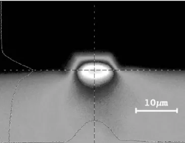
In most of the a-cut crystals the surface became brittle upon implantation. As shown in Fig. 1, striations [13], larger cracks, split-off islands and peeling-off of the surface layer
FIGURE 1 Optical micrograph of an a-cut crystal after the implantation with 2.4 MeV He+ ions. (a) Striations and split-off islands are visible. Fluence was 0.75 × 10¹⁶ions/cm2. (b) A larger crack runs horizontally through the photo. A layer peeled off, starting from the crack. Fluence was 1.5× 10¹⁶ions/cm2
developed with the growing implantation fluence. The thick-ness of the peeled-off layer did not always coincide with the implantation depth, but was in some cases∼ 2.5 times larger. No surface cracking was observed in the c-cut implanted crys-tals. Therefore, our research was focused on the development of waveguides in the c-cut crystals. Since the emission cross-section for theπ- transition (E||c) is ∼ 2.5 times higher than for theσ- transition (E⊥c), focus was put on the TM wave-guide modes.
Channel waveguides were fabricated out of planar wave-guides by photolithographic patterning and subsequent Ar+ sputtering. Since waveguide modes shift toward the optical barrier (see Sect. 3.1), a rib height close to the waveguide thickness is needed for complete lateral confinement of the propagating light. The achievable height of the smooth sput-tered ribs was 4–5µm, thus limiting the suitable planar wave-guide thickness to∼ 5 µm. We thinned the already available implanted planar waveguides from 6.5 µm down to ∼ 5 µm by Ar+ sputtering of the unmasked crystals. Essentially the same planar waveguides could also be fabricated directly by implanting the bulk crystals with ∼ 1.9 MeV He+ ions. As
FIGURE 2 SEM image of the fabricated rib structure. The He+stopping region is clearly recognizable as a sharp groove, separating the rib from the bulk. The waveguide cross section is trapezoidal with the width at the base w ∼ 11 µm, width on top d ∼ 9 µm and height h ∼ 5 µm
a first step of the rib fabrication, a 5.3 µm thick photoresist (PR) layer (Clariant AZ 4533) was spin-coated on top of the implanted crystal surface. Photoresist stripes of 11µm width were then formed by standard photolithography and hardened with a 30 min hardbake at 115◦C. After that, the PR pat-tern was transferred down to the Cr:LiSAF planar waveguide by Ar+sputtering (Oxford Plasmalab 80, RF power 300 W) and the 5.0 µm high ribs were finally fabricated. The sput-ter rates of the Cr:LiSAF and the PR mask were 3.9 nm/min and 1.9 nm/min, respectively. The obtained structures were investigated with a profilometer and a scanning electron mi-croscope (SEM). In Fig. 2 an SEM image of the fabricated rib waveguide with a polished end facet is shown. The He+ stop-ping region is clearly seen as a sharp groove, separating the rib from the bulk material.
3 Optical characterisation
3.1 Refractive index profile and propagation losses By TM dark mode spectroscopy using prism coup-ling we could determine the refractive index profile nein the
surface region of the crystal. The calculation method is pre-sented in more detail in [18]. Figure 3 shows a reconstructed refractive index profile that best matches the measured data, together with the mode curve of the measured and calculated waveguide modes. The FWHM of the calculated barrier is
∼ 0.5 µm, which is in agreement with the SRIM-2003
(stop-ping and range of ions in matter [19]) simulation. Comparison between the calculated index profile and the simulation of the implantation damage implies that the electronic energy loss (EEL) of He+ions shapes the nonuniform index profile in the wave-guiding layer. The EEL reaches its maximum at
∼ 3.5 µm and drops steeply afterwards. The nuclear energy
loss (NEL) occurs only at the end of the ion track and gives shape to the low-index optical barrier. In-between, there is a window of minimal combined loss (EEL and NEL) that re-sults in a smaller index decrease at∼ 5.5 µm. Consequently, the centre of the waveguide modes shifts toward the barrier (see Fig. 5).
In order to optimize the performance of a potential wave-guide laser or a broadband fluorescence source, the propaga-tion losses at both the pump wavelength and especially the
FIGURE 3 Refractive index profile for an implantation with 5× 10¹⁵ions/ cm2, measured at 633 nm. The data points represent the measured TM dark mode positions and the solid curve through them gives the theoretical mode positions corresponding to the shown fitted profile
emission wavelength should be as low as possible. Meas-urements of the planar waveguide propagation losses at the near-infrared (NIR) emission wavelength of 830 nm (close to the max. of fluorescence, see below) were performed using the end-coupling configuration. A tuneable Cr:LiSAF laser (IR-Point, Rainbow Photonics) was employed as the source of the probe beam. The transmitted waveguide output was se-lected with the aperture and measured with a silicon power meter. Two cylindrical lenses were used to focus the colli-mated beam in one plane and couple it into- and out of the pla-nar waveguide. The lowest propagation losses of 9±1 dB/cm (TM polarisation, assuming a coupling efficiency of 80%) were measured in the waveguides implanted with a fluence of 5× 10¹⁵ions/cm2. Relatively high losses are attributed
to the absorption due to implantation-generated colour cen-tres and to the tunnelling through the barrier. In order to reduce the losses due to absorption, the pulsed laser anneal-ing (PLA) technique was suggested in [13]. However, the PLA performed similarly as in [13] did not reduce the losses. It is believed that the ultraviolet light penetrated the crystal far beyond the wave-guiding layer and accordingly annealed the barrier as well. Alternatively, thermal annealing was per-formed for up to 10 h at∼ 210◦C. The measured losses de-creased for∼ 5%, which is still within the experimental error of the loss measurement.
Channel waveguides fabricated by etching techniques usually suffer from additional losses with respect to the pla-nar waveguides due to additional scattering on the waveguide sidewalls. The attenuation of the light propagating in the fabri-cated rib waveguides was measured by a similar end-coupling setup, in which the microscope objectives of magnification 10× were used to couple the light into- and out of the rib waveguides. The lowest value of the measured losses in
a 2.0 mm long crystal for TM polarised light at λ = 830 nm
was 10± 2.5 dB/cm, assuming a coupling efficiency of 80%. Because of strong tunnelling, the electric field of the light propagating in the waveguide extended significantly beyond the barrier. Comparison of the propagation losses in planar and channel waveguides suggests that surface scattering could have only a minor contribution (of< 1 dB/cm) to the overall propagation losses. Two major sources of losses were
tun-mode red laser diode (Opnext HL6526FM, max. 165 mW at 660 nm) was used as the optical pump source. The fluo-rescence emission from the exit facet of the waveguide was imaged by a microscope objective onto the spectrometer, CCD camera and silicon power meter, respectively. A long-pass filter was used to remove the residual pump radiation.
Figure 4 shows the measured spectra of the fluorescence light emitted from the waveguide and from the bulk crys-tal. The spectra differ only slightly, which suggests that the local environment of the active Cr3+ ions remained mostly
unaltered after the implantation. The spectrum width in the case of the waveguide was 75 nm FWHM, compared to 85 nm FWHM in the bulk material. The spectral distribution is nar-rower on the long wavelength side and the spectrum peak of the waveguide output is shifted for 7 to 803 nm. Both effects can be attributed to the comparatively higher tunnelling losses on the longer-wavelength side. The intensity profile of the flu-orescence emitted from the waveguide is shown in Fig. 5. The measured intensity profile is symmetrical and strongly con-fined in the horizontal direction as a consequence of the 5µm deep etching. The asymmetry in the vertical plane (⊥ to the implanted surface) is attributed to the nonuniform refractive index within the waveguide and to the leakage of light through the optical barrier into the bulk material.
The output power of the fluorescence emission as a func-tion of the input optical pump (Pp) power is shown in
Fig. 6. The maximal measured fluorescence output power was around 13µW at 165 mW input power. The crystal’s base surface was held at 6◦C. According to our estimation, the tem-perature in the front part of the waveguide rose to 60–100◦C for Pp= 100 mW. Therefore, we suppose that strong thermal
quenching occurred and suppressed the emission at higher
FIGURE 4 Measured spectrum of the fluorescence light emitted out of the waveguide (solid line) and the underlying bulk material (dashed line). The fluorescence spectrum of the waveguide remains predominantly unchanged
FIGURE 5 Fluorescence emission profile measured at the exit of the chan-nel waveguide. Waveguide dimensions as in Fig. 3
FIGURE 6 Emitted fluorescence power as a function of the input optical pump power. The line connecting the measurement points is a guide to the eye. The actual in-coupled pump power is∼ 0.7× input power. Dimensions of the waveguide: cross-section as in Fig. 3, length is 2.0 mm
input powers. This would explain why the slope efficiency decreased from∼ 15 × 10−5to∼ 4 × 10⁻⁵with increasing in-put power. Polarisation ratio of the emitted fluorescence was
Ic: Ia≈ 2.4 : 1, which is in agreement with the ratio of the corresponding emission cross-sections in a bulk crystal [3].
Additionally, the NIR probe beam was coupled simultan-eously with the pump beam into the waveguide and the op-tical amplification of the NIR light was measured. The NIR power before the first microscope objective was 2.1 mW, the out-coupled power was 0.82 mW, which gave a propagation loss of 10.3 dB/cm for that particular waveguide. The rise of the NIR output with increasing optical pump is shown in Fig. 7. The out-coming NIR increased nearly proportionally to the input optical pump until Pp∼ 70 mW, after which it
remained constant, within the measurement error. We simu-lated NIR amplification along the waveguide with a simplified one-dimensional numerical model using the laser rate equa-tions. The measurement data were in good agreement with the model for the product nt× τfbeing approximately 20–25 times smaller than the nt0× τf0 of the bulk material, where, nt is the density andτfis the fluorescence lifetime of the
ac-tive Cr3+ions in the waveguide, respectively. We believe that
due to a temperature increase within the waveguide the major
FIGURE 7 Measured and simulated transmitted NIR light as a function of input pump power. The waveguide is the same as in Fig. 6
contribution to the drop of nt× τfcame from a smaller fluo-rescence lifetime due to thermal quenching, at least at higher optical pump powers.
4 Conclusion
Cr:LiSAF channel waveguides have been fabri-cated by He+ implantation and Ar+sputtering. The wave-guides supported NIR optical mode propagation with mod-erate propagation losses. The two major sources of propaga-tion losses were found to be tunnelling through the optical barrier and absorption due to colour centres. Losses in the channel waveguides did not increase significantly with re-spect to the ones in planar waveguides due to the smooth rib surface of the channel waveguides. The fluorescence emit-ted from the optically pumped waveguides was spatially well confined and had a wide spectrum ranging from 760 nm to 900 nm. Therefore, we expect that such devices could be considered as the fluorescence source in low-coherence in-terferometry where high longitudinal resolution is needed. The fluorescence output power in these proof-of-concept ex-periments was up to 13µW at 165 mW of pump power. The output power could be further increased by optimising the optical barrier and by a more efficient annealing. Thermal quenching was the most probable cause that limited the out-put power. Attaching a clad waveguide directly to a heat sink could significantly diminish thermal quenching and al-low a further increase of the emitted fluorescence output power.
ACKNOWLEDGEMENTS The authors thank J. Hajfler for polishing the crystals. This work was partially supported by the Swiss Inno-vation Promotion Agency (KTI Nr. 4753.1 SUS-NM).
REFERENCES
1 A.M. Kowalevicz, T. Ko, I. Hartl, J.G. Fujimoto, M. Pollnau, R.P. Salath´e, Opt. Express 10, 349 (2002)
2 D. Huang, E.A. Swanson, C.P. Lin, J.S. Schuman, W.G. Stinson, W. Chang, M.R. Hee, T. Flotte, K. Gregory, C.A. Puliafito, J.G. Fuji-moto, Science 254, 1178 (1991)
3 S.A. Payne, L.L. Chase, L.K. Smith, W.L. Kway, H.W. Newkirk, J. Appl. Phys. 66, 1051 (1989)
4 M. Stalder, M. Bass, B. H T. Chai, J. Opt. Soc. Am. B 9, 2271 (1992) 5 S. Uemura, K. Miyazaki, Japan. J. Appl. Phys. 36, 4312 (1997) 6 S.A. Payne, L.K. Smith, R.J. Beach, B.H.T. Chai, J.H. Tassano, L.D.
De-Loach, W.L. Kway, R.W. Solarz, W.F. Krupke, Appl. Opt. 33, 5526 (1994)