HAL Id: hal-00394756
https://hal.archives-ouvertes.fr/hal-00394756
Submitted on 21 Oct 2013
HAL is a multi-disciplinary open access
archive for the deposit and dissemination of
sci-entific research documents, whether they are
pub-lished or not. The documents may come from
teaching and research institutions in France or
abroad, or from public or private research centers.
L’archive ouverte pluridisciplinaire HAL, est
destinée au dépôt et à la diffusion de documents
scientifiques de niveau recherche, publiés ou non,
émanant des établissements d’enseignement et de
recherche français ou étrangers, des laboratoires
publics ou privés.
Ultracompact silicon-on-insulator ridge-waveguide
mirrors with high reflectance
Philippe Velha, Jean-Claude Rodier, Philippe Lalanne, Jean-Paul Hugonin,
David Peyrade, Eric Picard, Thomas Charvolin, Emmanuel Hadji
To cite this version:
Philippe Velha, Jean-Claude Rodier, Philippe Lalanne, Jean-Paul Hugonin, David Peyrade, et al..
Ultracompact silicon-on-insulator ridge-waveguide mirrors with high reflectance. Applied Physics
Letters, American Institute of Physics, 2006, 89 (17), pp.171121. �10.1063/1.2372581�. �hal-00394756�
Ultracompact silicon-on-insulator ridge-waveguide mirrors
with high reflectance
P. Velha,a兲 J. C. Rodier, P. Lalanne,b兲and J. P. Hugonin
Laboratoire Charles Fabry de l’Institut d’Optique, Centre National de la Recherche Scientifique, Université Paris-Sud, Campus Polytechnique, RD 128, 91127 Palaiseau Cedex, France
D. Peyrade
Laboratoire des Technologies de la Microélectronique, Centre National de la Recherche Scientifique, UMR5129, 17 rue des Martyrs, 38054 Grenoble Cedex 9, France
E. Picard, T. Charvolin, and E. Hadji
Laboratoire Silicium Nanoélectronique Photonique et Structure, Département de Recherche Fondamentale sur la Matière Condensée, Commissariat à l’Energie Atomique, 17 rue des Martyrs, F-38054 Grenoble Cedex, France
共Received 10 March 2006; accepted 20 September 2006; published online 27 October 2006兲 Microcavities offering small modal volumes V⬇ 0.6 共 / n兲3
and consisting of two identical tapered Bragg mirrors etched into a monomode silicon-on-insulator ridge waveguide are studied for operation at telecommunications wavelengths. The authors have measured a Q factor of 8900, for a loaded cavity with a peak transmission at resonance in excess of 60%. The measured Q value quantitatively agrees with the calculation results and is 20 times larger than those previously reported for similar geometries without tapers. © 2006 American Institute of Physics.
关DOI:10.1063/1.2372581兴
High-Q optical microcavities, which confine light in wavelength-sized modal volumes V, are essential compo-nents of many optical devices and effects, from spontaneous-emission inhibition or enhancement,1 threshold laser reduc-tion, to a wide range of processing functions in integrated systems.2Light confinement can be achieved by total internal reflection共TIR兲, Bragg reflection, or a combination of both mechanisms. In ring or disk resonators, confinement solely relies on TIR. These microcavities can be cascaded to imple-ment various optical functions,3,4and with strong lateral con-finement as in silicon-on-insulator共SOI兲 substrates, the disk or the ring resonators can have a very small共1 – 3m兲 di-ameter with small bending loss.2 Microcavities in two-dimensional photonic-crystal共PC兲 slabs are also highly valu-able candidates for achieving high Q’s and small V’s. Presently, Q factors above 105with wavelength-sized V’s are
available in several research laboratories, see Refs.5 and6
and references therein. However, these recorded Q values are obtained by etching off the sacrificial buried layer under the PC slab to form a suspended membrane in air. This puts severe restrictions on large-scale integration. Apparently, achieving high-Q PC microcavities on a substrate is not ob-vious: as shown in a recent report,7 PC cavities with Q = 5000 in a silicon membrane offer Q values ten times smaller once implemented without removing the SiO2layer.
The microcavities considered in this work are fabricated in a SOI substrate. For integrated photonics, silicon is an ideal material platform because of its maturity in the elec-tronics industry, offering the possibility to combine both photonic and electronic devices all on one chip. Like ring resonators, a classical translation-invariant ridge waveguide is used to confine light in the transversal directions. The
longitudinal confinement is achieved by mirrors composed of subwavelength holes, like in PC cavities. In comparison with earlier works on similar geometries,8–10 the mirrors are not fully periodic. Through a fine geometry tuning designed with Bloch-mode-engineering concepts,11,12 they additionally in-corporate a taper section composed of four holes, see Fig.1. The taper section aims at reducing the transverse-mode-profile mismatch at the interface between the periodic sec-tion of the mirrors and the ridge waveguide, and thus at canceling out-of-plane radiation losses. A Q factor of 8900 has been measured at midgap frequency共 = 1.58m兲 for a loaded cavity with a peak transmission larger than 60%. The measured Q value represents a 20-fold improvement over previously reported Q’s for similar in-line geometries8–10or over three-hole-missing two dimensional photonic-crystal cavities recently fabricated on a SiO2substrate.
7
The cavity structures are fabricated from SOI wafers with a 340 nm single crystal Si layer on a 2m SiO2layer.
The ridge and hole patterning is performed by electron-beam lithography with a Leica VB-6UHR vector scan generator in a 400-nm-thick NEB22 negative resist spin coated on the
a兲Also at Laboratoire des Technologies de la Microélectronique and CEA Laboratory SiNaPS.
b兲
Electronic mail: philippe.lalanne@iota.u-psud.fr
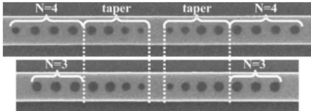
FIG. 1. SEM photographs of two microcavities considered in this work. The Bragg mirrors are composed of a four-hole taper and of a periodic section with N holes共N = 3 and 4 in the photographs兲. The taper hole diameters, measured with the SEM, are 130, 160, 185, and 181 nm with center-to-center hole distances of 300, 315, 325, and 352 nm. The periodic section of the mirrors is composed of holes with a 181 nm diameter and the periodicity constant is a = 370 nm. The side-to-side distance between the two inner holes共the physical length of the cavities兲 is L = 425 nm.
APPLIED PHYSICS LETTERS 89, 171121共2006兲
0003-6951/2006/89共17兲/171121/3/$23.00 89, 171121-1 © 2006 American Institute of Physics
sample. After developing the resist, etching is performed in an inductively coupled industrial plasma chamber共DPS from Applied Materials Inc.兲. The silicon layer is then etched with a Cl2, HBr, and O2 gas mixture, using the SiO2 layer as an
etch stop. Finally, resist is stripped by oxygen plasma. For testing purposes, the wafer is manually cleaved to obtain optical facets. The lengths of the two access ridge waveguides are approximately 7 and 3.5 mm, respectively. Several cavities with identical taper sections, but with a dif-ferent number共N = 2, 3, and 4兲 of holes in the periodic sec-tion, are fabricated on the same wafer. Because they are dif-ficult to characterize with our in-line characterization setup, cavities with N = 5 have not been fabricated. The layout also includes reference ridge waveguides 共without cavities兲 for characterization purposes.
After fabrication, the cavities are first observed with a scanning electron microscope 共SEM兲. Microcavity SEM photographs are shown in Fig.1. The ridge width is 520 nm and typical hole diameters vary from 130 to 190 nm. The wafer is also observed with an atomic force microscope 共AFM兲, revealing that the surface roughness of the ridge sidewalls is⬇3 nm rms. The device under test is mounted on an, XYZ translational stage. TE-polarized light from a high-resolution tunable external laser source共1520– 1620 nm兲 is launched into the 7-mm-long access waveguide using a polarization-maintaining fiber connected to a microlensed fi-ber. The fiber tip produces a spot with a beam waist of ⬇2.1m with minimal mixing of TE-TM modes共rejection ratio of 20– 30 dB兲. After passing through the device, the light is collected by an imaging system composed of a ⫻20 microscope objective共numerical aperture of 0.30兲 and of an antireflection coated planoconvex lens with a 50 mm focal length. The waveguide output is imaged either onto an IR camera for observing light at the output cleaved facet or onto an InGaAs photodiode for quantitative transmission mea-surements. Additionally, when using the InGaAs photodiode, the imaging system incorporates a 100m pinhole and a polarizer in order to filter the inevitable spurious substrate-guided light.
We first estimate the attenuation loss of the ridge waveguides. Five reference waveguides, without cavities, are characterized by measuring the contrast of the Fabry-Perot fringes resulting from the bouncing of light between the cleaved facets. Assuming a facet modal reflectivity of 0.36, a value calculated with a fully vectorial three dimensional 共3D兲 Fourier modal method, we obtain a straight-waveguide-attenuation loss of 6 ± 1 dB/ cm. This value is compatible with the sidewall roughness measured with the AFM共Ref.
13兲 and is only twice larger that the best attenuation reported so far for similar SOI ridge geometries.14
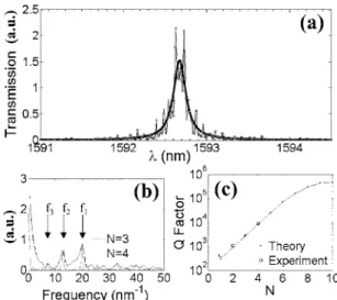
The main results obtained for cavity-transmission mea-surements are summarized in Fig. 2. The dots in Fig. 2共a兲
represent the transmission spectrum recorded for the cavity with N = 4. The data exhibit high-frequency oscillations, with large amplitudes at resonance. The oscillations can be easily interpreted by considering that the analyzed system is actu-ally composed of three coupled cavities, the microcavity un-der study and two additional cavities formed by the cleaved facets and the microcavity itself. The solid curve in Fig.2共b兲
shows the Fourier transform of the recorded spectrum. Three peaks at frequencies, labeled f1, f2, and f3 in the figure, are
observed. These peaks also show up in the Fourier spectrum 共dashed curve兲 of the cavity with N = 3. The two first
fre-quencies are due to the bouncing of light in the two access waveguides, and the third one represents the frequency dif-ference f1− f2. As can be easily shown by analytic
consider-ations, it is impossible to extract the Q factor of the micro-cavity from the sole knowledge of the transmission of the coupled-cavity system. Additional information, such as the knowledge of the peak transmission Tmax at resonance, is
required. Nevertheless, to estimate the microcavity Q, we apply a low pass filter, filtering out all frequencies above f3.
After fitting to a Lorentzian function, we obtain the thick solid curve in Fig.2共a兲, and a Q factor of 8900 is inferred. Simulations performed with a 2 ⫻ 2 transfer-matrix approach have shown that the filtering technique generally underesti-mates the microcavity Q factors. The relative difference may be as large as 20% for large Fabry-Perot oscillation ampli-tudes as those in Fig.2共a兲. The same characterization proce-dure has been performed for microcavities with N = 2 and 3 holes in the periodic sections of the mirrors. The measured Q values are reported in Fig.2共c兲as squares.
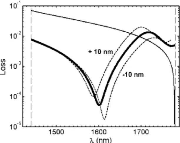
In order to obtain more in-depth insight into the experi-mental results and the tapering effect, we have computed the modal reflectivities RNof the tapered mirrors for several
val-ues of the number N of holes in the periodic section of the mirrors. The computations are performed with a 3D fully vectorial frequency-domain Fourier modal method15for geo-metric dimensions measured on the actual device, see the caption of Fig.1for details. The thick curve in Fig.3shows 1 − R⬁ over the 350-nm-wide mirror-band gap centered
around = 1.55m. For semi-infinite mirrors 共N = ⬁兲, 1 − R⬁represents the radiation loss in the cladding due to the
mode-profile mismatch at the mirror interface. Because the SEM technique used to determine the hole diameters has a limited accuracy of ±5 nm, we have also performed compu-tations for mirror geometries obtained by increasing or de-creasing all hole diameters by 10 nm, while keeping un-changed the center-to-center hole distances. The results, shown with the dashed curves in Fig.3, clearly indicate that
FIG. 2. Experimental results and data analysis.共a兲 Recorded transmission spectrum共in arbitrary units兲 of the microcavity with N = 4 holes in the pe-riodic section of the mirror. The high-frequency oscillations are Fabry-Perot fringes due to the bouncing of light between the cleaved facets. The solid bold curve is obtained after filtering.共b兲 Fourier transform of the cavity transmissions for the N = 4 cavity 共solid curve兲 and for the N = 3 cavity 共dashed curve兲. 共c兲 Comparison between the measured and calculated Q factors as a function of N. Squares: experimental data. Dots: Q values ob-tained with the Fabry-Perot model from modal reflectivities RNcalculated for geometric dimensions measured on the actual device.
171121-2 Velha et al. Appl. Phys. Lett. 89, 171121 共2006兲
this uncertainty does not impact the analysis. They also evi-dence that the tapering process is tolerant to fabrication er-rors. At midgap frequency 共 ⬇ 1.6m兲, the losses of the tapered mirror共solid bold curve兲 are very small ⬇5 ⫻ 10−5, a
value 400 times lower than that obtained without taper with the fully periodic mirror 共thin-solid curve兲. We have also performed similar computations for mirrors with a finite number N of holes. From these calculations, the theoretical cavity Q’s are deduced by using a Fabry-Perot model, Q =/共1 − RN兲关2共L / 0兲ng−共0/兲共N/兲0兴, where ng= 4.12
is the group index of the fundamental ridge-waveguide mode, L is the cavity defect length 共side-to-side separation distance between the two inner holes兲, andNis the phase of
the modal reflectivity coefficient. For = 1.6m, Q = 19.6/共1 − RN兲, and we find that the measured Q of 8900 for
the cavity with N = 4 corresponds to a finesse F =/共1 − RN兲
equal to 1400. The dots in Fig.2共c兲represent the Q values computed with the Fabry-Perot model. An excellent agree-ment with the experiagree-mental data共squares兲 is seen. We have also calculated the cavity mode volume with the Fourier modal method. We found that the mode volume V, defined by V =兰兩E兩2dV/ max共兩E兩2兲 共E being the electric field of the
cavity mode兲, is equal to 0.62 共 / n兲3. Such a small value is
due to the strong TIR transversal confinement and, longitu-dinally, to the taper-design strategy which relies only on the use of mirrorlike nonpropagating Bloch modes in the taper, thus not only the taper implements a transverse-mode-profile conversion but it also reflects light.12
The peak transmission Tmaxat resonance is another
im-portant figure of merit. For a Fabry-Perot cavity, one expects that Tmax=共1 + L / T兲−2, where T is the mirror in-plane modal
transmission, and L = 1 − R − T is the mirror loss 共radiation into the cladding in the present case兲. The measurement of
Tmaxis critical. We have recorded several times the
transmis-sion spectrum of the reference waveguides and that of the
N= 4 cavity, systematically realigning the microlensed fiber with the waveguide input facets before recording. From these
spectra, we could not infer the actual Tmax value but we
could derive a lower bound, Tmax⬎0.6共the theoretical Tmax
value is 0.99 at = 1.6m兲. The prediction of a high Tmax
value for the N = 4 cavity is consistent with other measure-ments performed for cavities with N = 2 and 3, since we do not observe any significant decrease of the peak transmis-sions as N increases, the slight fluctuations being well within the uncertainty of the repeatability of the injection into the cleaved facet. In other words, the mode lifetime of the N = 4 cavity is likely to be limited by in plane transmission rather than radiation loss 共T ⬎ L兲. From the Fabry-Perot model, a Tmax value larger than 0.6 implies that T ⬎ 3.4L.
Thus the intrinsic共unloaded兲 Q factor of the cavity, deter-mined by removing the coupling between the waveguide and the cavity 共N = ⬁兲, is expected to be larger than 40 000, a value ten times smaller than the theoretical prediction shown in Fig.2共c兲.
In summary, ultrashort and highly efficient Bragg mir-rors incorporating taper sections have been fabricated in ridge SOI waveguides and have been characterized at tele-communications wavelengths. Microcavities formed by the association of two identical mirrors have been studied. A Q factor of 8900 has been measured for a cavity with a mode volume of 0.62共 / n兲3. The measured Q value is the highest
reported so far for cavities 共with comparable small mode volumes兲 manufactured on a substrate. Due to their large finesses, these cavity geometries may be useful for different applications, including Si electro-optic modulators16or filters for wavelength divison multiplexing applications.
CEA-LETI is acknowledged for the access to the micro/ nanofabrication facilities. This work is supported under the project Miraman PNANO06-0215. One of the authors共P.V.兲 acknowledges support from CNRS and CEA for his Ph.D. Fellowship.
1
K. J. Vahala, Nature共London兲 424, 839 共2003兲. 2
B. E. Little, Opt. Photonics News, November 2000, p. 24. 3
J. Poon, L. Zhu, G. DeRose, and A. Yariv, Opt. Lett. 31, 456共2006兲. 4
A. Melloni and M. Martinelli, J. Lightwave Technol. 20, 296共2002兲. 5
Y. Tanaka, T. Asano, R. Hatsuta, and S. Noda, Appl. Phys. Lett. 88, 011112共2006兲.
6
R. Herrmann, T. Sünner, T. Hein, A. Löffler, M. Kamp, and A. Forchel, Opt. Lett. 31, 1229共2006兲.
7
Y. Tanaka, T. Asano, R. Hatsuta, and S. Noda, Appl. Phys. Lett. 88, 011112共2006兲.
8
J. P. Zhang, D. Y. Chu, S. L. Wu, W. G. Bi, R. C. Tiberio, R. M. Joseph, A. Taflove, C. W. Tu, and S. T. Ho, IEEE Photonics Technol. Lett. 8, 491 共1996兲.
9
D. J. Ripin, K. Y. Lim, G. S. Petrich, P. R. Villeneuve, S. Fan, E. R. Thoen, J. D. Joannopoulos, E. P. Ippen, and L. A. Kolodziejski, J. Appl. Phys. 87, 1578共2000兲.
10
A. S. Jugessur, P. Pottier, and R. M. De La Rue, Electron. Lett. 39, 367 共2003兲.
11
P. Lalanne and J. P. Hugonin, IEEE J. Quantum Electron. 39, 1430共2003兲. 12
C. Sauvan, G. Lecamp, P. Lalanne, and J. P. Hugonin, Opt. Express 13, 245共2005兲.
13
S. Lardenois, D. Pascal, L. Vivien, E. Cassan, S. Laval, R. Orobtchouk, M. Heitzmann, N. Bouzaida, and L. Mollard, Opt. Lett. 28, 1150共2003兲. 14
Y. A. Vlasov and S. J. McNab, Opt. Express 12, 1622共2004兲. 15
E. Silberstein, P. Lalanne, J. P. Hugonin, and Q. Cao, J. Opt. Soc. Am. A
18, 2865共2001兲. 16
Q. Xu, B. Schmidt, S. Pradhan, and M. Lipson, Nature共London兲 435, 325 共2005兲.
FIG. 3. Beneficial impact of the tapering process on the mirror performance. The bold共thin兲 solid curves correspond to calculated radiation losses 共de-fined as 1 − R⬁兲 for tapered 共periodic兲 semi-infinite mirrors 共N = ⬁兲. The loss spectra are calculated from dimensions measured on the actual devices, as given in the caption of Fig.1. The thin-dashed curves are obtained for mirrors with a ± 10 nm variation of all hole diameters, and the vertical dashed lines indicate the band edges of the periodic mirror.
171121-3 Velha et al. Appl. Phys. Lett. 89, 171121 共2006兲