HAL Id: tel-02328582
https://tel.archives-ouvertes.fr/tel-02328582
Submitted on 23 Oct 2019HAL is a multi-disciplinary open access archive for the deposit and dissemination of sci-entific research documents, whether they are pub-lished or not. The documents may come from teaching and research institutions in France or abroad, or from public or private research centers.
L’archive ouverte pluridisciplinaire HAL, est destinée au dépôt et à la diffusion de documents scientifiques de niveau recherche, publiés ou non, émanant des établissements d’enseignement et de recherche français ou étrangers, des laboratoires publics ou privés.
phénomènes de piégeages affectant la fiabilité des
technologies CMOS avancées (Nanofils) 10nm
Artemisia Tsiara
To cite this version:
Artemisia Tsiara. Caractérisations électriques et modélisation des phénomènes de piégeages af-fectant la fiabilité des technologies CMOS avancées (Nanofils) 10nm. Micro and nanotechnolo-gies/Microelectronics. Université Grenoble Alpes, 2019. English. �NNT : 2019GREAT010�. �tel-02328582�
Pour obtenir le grade de
DOCTEUR DE LA COMMUNAUTE UNIVERSITE
GRENOBLE ALPES
Spécialité : Nano électronique et Nano technologie
Arrêté ministériel : 25 mai 2016
Présentée par
Artemisia TSIARA
Thèse dirigée par Dr. Gérard GHIBAUDO, IMEP-LAHC, et codirigée par Dr. Xavier Garros, CEA-LETI
préparée au sein du CEA-LETI et de l’IMEP-LAHC dans l'École Doctorale Electronique, Electrotechnique, Automation et Traitement du Signal
Electrical characterization &
modeling of the trapping
phenomena impacting the
reliability of nanowire transistors
for sub 10nm nodes
Thèse soutenue publiquement le 6 Mars 2019, devant le jury composé de :
Monsieur Françis BALESTRA
Directeur de recherche, CNRS, Président de jury Monsieur Olivier BONNAUD
Professeur, Université de Rennes 1, Rapporteur Madame Nathalie MALBERT
Professeur, Université Bordeaux, Rapporteur Monsieur Xavier GARROS
Ingénieur, CEA-LETI, Co-Encadrant (Invité) Monsieur Gérard GHIBAUDO
5
Acknowledgements
Surprisingly enough, this appears to be the most difficult part of this manuscript, not really knowing what is appropriate to write about the end of an era, a.k.a. PhD, but I’ll give it a go!
First of all, this work was made possible through the collaboration between CEA-Leti (LCTE laboratory) and IMEP-LaHC, under the financial support of LabEx Minos ANR-10-LABX-55-01 program that I thank very much for helping towards the realization of this project.
I would like to start my acknowledgements by thanking the reading committee, Madame Nathalie Malbert et Monsieur Olivier Bonnaud for accepting to be members of my jury and for spending time to provide their invaluable insight and comments on the manuscript, as well as to Monsieur Françis Balestra for being the president on my defense day.
My warmest thanks to my academic supervisor, Directeur de Recherche, Gérard Ghibaudo for choosing me as a student and for being there every time I needed him. His level of ‘coolness’ matches his immense knowledge on nanoelectronics!
A big shout out to Xavier Garros, my daily supervisor, my guide and mentor on reliability. Your patience, persistence and multitasking ability has helped me graduate from the famous X-academy (all right reserved!). Huge gratitude for everything you taught me and for constantly having time for me even when you didn’t.
Many thanks to all the older and newer members of the LCTE laboratory for all the interaction we had during these last 3 years, the time we shared together and your support.
To my two exceptional French friends, Antoine Laurent and Alexandre Vernhet! Antoine, you welcomed me in B261 since day 1 2 and I cannot really choose only one thing to be grateful for. Thank you for all the laughs and very rare serious discussions we had, for all the comics you were lending me to read and for my French that never improved since we never really used it. Please be careful when you play football, you have a daughter to take care of now! To Alex, the greatest Pythonista of all time and a walking google database, I will miss you so much. I still need to find someone that insults my Greek culture and to bother when I have any kind of questions. Thank you for everything! To the Brazilian goddess, Brun(it)a, it was a real joy to meet you in Grenoble, despite the cold weather that made our stay more difficult! Thank you for all the time we spend together, for coming to France for a third time and I wish you all the best for the future! Stay in Europe girl! I’m waiting all of you in Belgium/ flat land for a degustation of all the available beers in the country (Bruna it’s chocolate and waffles for you)!
Many thanks to a new colleague at imec, Emmanuel Chery for all the time he spent helping me with the dry runs of my defense and the correction of my French resume! Couldn’t have been properly prepared without you!
Φυσικά και θα σου αφιέρωνα ξεχωριστή παράγραφο, ας είμαστε σοβαροί! Αν και δε συγκρατώ ονόματα το ξέρεις, Κωνσταντίνε Τριαντόπουλε! :) Καταρχάς σταμάτα να διαβάζεις τις βλακείες που γράφω παραπάνω και έλα κατά δω. Ας σοβαρευτώ για λίγο λέγοντας σου ότι ειλικρινά δε ξέρω πως τη πάλεψα τη πρώτη χρονιά του διδακτορικού στο χωρζιό και
6 μπ@#$%λο που δεν ήσουν εδώ (αν κάτι μισώ είναι οι ερασιτεχνισμοί και η μιζέρια). Σ’ευχαριστώ για όλα, που είσαι αυτός που είσαι, που είμαστε φιληνάδες, όμορφες, κοπέλες, κολλητούλες. Σταμάτα να αγοράζεις στυλό και τετράδια και προετοίμασε τον λόγο σου όταν θα κάνεις τις ανακοινώσεις για τα επόμενα επαγγελματικά σου βήματα. Εσείς εδώ τι κάνετε, με τι ασχολείστε τέλος πάντων? Λίγο έμεινε κ ετοιμάζεσαι για αποχώρηση, άντε με έχεις αφήσει σαν τη χήρα να τριγυρνάω εδώ πέρα. Εμείς σπίτι, άντρα δεν έχουμε? Μεγάλο ευχαριστώ σε όλους τους φίλους μου, παλιότερους και νέους: Τάσα που είσαι πάντα δίπλα μου ακόμα και από μακριά (15 χρόνια είναι αυτά, ακόμα να με στεφανωθείς!), Χριστίνα συνβασανισμένη δόκτωρ πλέον επί γαλλικού εδάφους, Ιωάννα doctor to be (διάλεξες κ εσύ την επιστήμη πανάθεμα σε, δε πήγαινες για μαλλάκια-νυχάκια). Σε νομό Θεσσαλονίκης, Κοζάνης, Καστοριάς, Αιτ/νίας, οι αγαπημένες μου πόλεις, πολλά ευχαριστώ για όλα! Και κάπου εδώ τελείωνουν οι ευχαριστιές με τους πιο σημαντικούς. Ένα μεγάλο ευχαριστώ στους γονείς μου, Βάσω και Σωκράτης, και στις μοναδικες αδερφές μου, Θάλεια και Δήμητρα, που ήταν πάντα εκεί για μένα και με στήριξαν όλα τα χρόνια που αποφάσισα να κυνηγήσω αυτό που ήθελα. Στη δεύτερη οικογένειά μου στη Θεσσαλονίκη, μόνο τεράστια ευγνωμοσύνη για όλα όσα μου έχουν δώσει και πάνω απ’ όλα για την αγάπη τους. Τελευταίος και καλύτερος, Κώστα χωρίς εσένα δε θα είχα κάνει το βήμα να φύγω για το διδακτορικό. Ακόμα και όταν όλα είναι μεταβλητά, εσύ είσαι το σημείο αναφοράς μου σ’αυτή τη ζωή. Σ’ ευχαριστώ για όλα..
7
Glossary
Abbreviation Description
AVGP Arbitrary VG Pattern
BL Bottom-Level
BOX Buried Oxide Layer
CCDF Complementary Cumulative Distribution Function
CDF Cumulative Distribution Function
CET Capture and Emission Time
CMOS Complementary Metal Oxide Semiconductor
CNF Carrier Number Fluctuations
CNF/CMF Carrier Number Fluctuation/ Correlated Mobility Fluctuation
CNT Carbon nanotubes
CP Charge Pumping
CV Capacitance-Voltage
DCM Defect Centric Model
DF Duty Factor
DIBL Drain-Induced Barrier Lowering
DV Dynamic Variability
EOT Equivalent Oxide Thickness
ESR Electron Spin Resonance
FDSOI Fully Depleted Silicon-On-Insulator
FEOL Front End of the Line
FFT Fast Fourier Transform
GAA Gate-All-Around
HCI Hot Carrier Injection
HK/MG High-k/Metal Gate
HMF Hooge Mobility Fluctuations
HRTEM High-Resolution Transmission Electron Microscopy
HT High Temperature
IL Interface Layer
ITRS International Technology Roadmap for Semiconductors
LFN Low Frequency Noise
LT Low Temperature
MC Monte Carlo
MOSFET Metal Oxide Semiconductor Field Effect Transistor
MSM Measure-Stress-Measure
NBTI Negative Bias Temperature Instability
PBTI Positive Bias Temperature Instability
8
PNA Post Nitridation Anneal
PSD Power Spectral Density
R-D Reaction-Diffusion
RSU Remote-sense and Switch Unit
RTN Random Telegraph Noise
S/D Source/Drain
SCE Short-Channel Effects
SMS Stress-Measure-Stress
SOI Silicon-On-Insulator
SW Side Walls
TB Thermal Budget
TDDB Time Dependent Dielectric Breakdown
TDDS Time Dependent Defect Spectroscopy
TEM Transmission Electron Microscopy
TL Top-Level
TS Top Surface
TSV Through Silicon Via
TTF Time-To-Failure
WF Work Function
9
Contents
ACKNOWLEDGEMENTS ... 5 GLOSSARY ... 7 CONTENTS ... 9 GENERAL CONTEXT ... 11 CHAPTER 1. INTRODUCTION ... 131.1 ISSUES ON CONVENTIONAL PLANAR TECHNOLOGIES... 13
1.1.1 EQUIVALENT SCALING OPPORTUNITIES ... 13
1.1.2 SOI PROCESS ... 14
1.1.3 3D ARCHITECTURES ... 15
1.1.4 NEW MATERIALS ... 15
1.1.5 3D SEQUENTIAL INTEGRATION ... 17
1.2 OXIDE DEFECTS OVERVIEW... 18
1.2.1 FIXED OXIDE CHARGE ... 18
1.2.2 MOBILE OXIDE CHARGE ... 19
1.2.3 OXIDE TRAPPED CHARGE ... 19
1.2.4 INTERFACE TRAPPED CHARGE ... 19
1.2.5 BORDER TRAPS ... 20
1.3 BIAS TEMPERATURE INSTABILITY ... 20
1.3.1 BTI DEGRADATION ... 21
1.3.2 REACTION-DIFFUSION MODEL ... 22
1.3.3 HUARD’S MODEL ... 23
1.3.4 GRASSER’S MODEL ... 23
1.4 CHARACTERIZATION OF AVERAGING EFFECT ... 24
1.4.1 DC STRESS ... 24
1.4.2 AC STRESS ... 27
1.5 CHARACTERIZATION OF INDIVIDUAL DEFECTS ... 28
1.5.1 RANDOM TELEGRAPH NOISE –LOW FREQUENCY NOISE (STATIONARY METHOD) ... 29
1.5.2 TIME DEPENDENT DEFECT SPECTROSCOPY ... 34
1.5.3 CORRELATION BETWEEN STANDARD NBTI TESTS AND TDDS ... 38
CHAPTER 2. IMPACT OF 3D ARCHITECTURES ON BTI/RTN RELIABILITY ... 39
2.1 INTRODUCTION ... 39
2.2 TESTED STRUCTURES ... 39
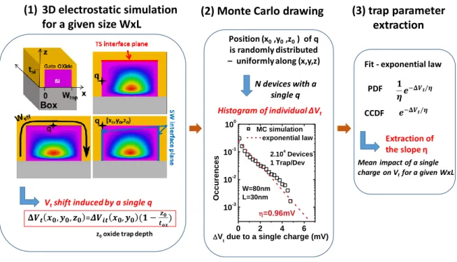
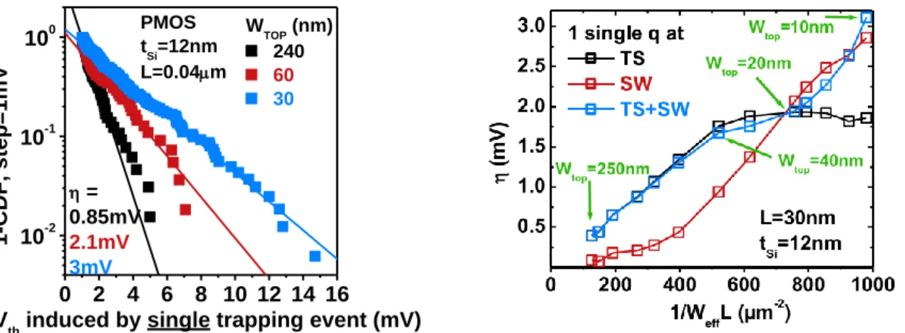
2.3 3D ELECTROSTATIC SIMULATION OF THE IMPACT OF ONE CHARGE ON VTH ... 39
2.4 RELIABILITY OF PMOS TRANSISTORS ... 40
2.4.1 EFFECT OF TOP WIDTH ... 40
2.4.2 EFFECT OF GATE LENGTH ... 41
10
2.5 COMPARISON OF TDDS AND RTN ... 44
2.5.1 SETUP PROCEDURE ... 45
2.5.2 COMPARISON METHOD ... 45
2.5.3 FRESH DEVICES ... 47
2.5.4 “AFTER STRESS” COMPARISON ... 50
CHAPTER 3. IMPACT OF 3D SEQUENTIAL INTEGRATION ON BTI/RTN RELIABILITY ... 55
3.1 INTRODUCTION ... 55
3.2 IMPACT OF LOW TEMPERATURE PROCESS ... 55
3.2.1 QUALITY OF THIN GATE STACK OXIDE ... 55
3.2.2 QUALITY OF THICK GATE STACK OXIDE ... 61
3.3 IMPACT OF DIFFERENT PROCESS STEPS ... 63
3.3.1 TESTED STRUCTURES ... 63
3.3.2 NITRIDATION ... 64
3.3.3 POST NITRIDATION ANNEAL ... 66
3.3.4 FORMING GAS ANNEAL ... 69
3.4 FULLY INTEGRATED 3D SEQUENTIAL TECHNOLOGY ... 71
3.4.1 DESCRIPTION-DEVICES ... 71
3.4.2 PERFORMANCE BOTTOM LEVEL ... 72
3.4.3 PERFORMANCE OF TOP LEVEL ... 75
3.4.4 RELIABILITY BOTTOM LEVEL ... 76
3.4.5 RELIABILITY TOP LEVEL ... 78
3.4.6 CIRCUIT LEVEL ... 79
CHAPTER 4. IMPACT OF HIGH MOBILITY MATERIALS ON NBTI RELIABILITY ... 85
4.1 INTRODUCTION ... 85
4.2 TESTED STRUCTURES ... 85
4.3 STUDY ON GO1 AND GO2 SHORT CHANNEL DEVICES ... 88
4.3.1 STANDARD NITRIDATION ... 88
4.3.2 HIGH NITRIDATION ... 89
4.4 STUDY ON GO1 AND GO2 LONG CHANNEL DEVICES ... 91
4.4.1 STANDARD NITRIDATION ... 91 4.4.2 HIGH NITRIDATION ... 92 GENERAL CONCLUSIONS ... 97 REFERENCES ... 101 PUBLICATIONS ... 113 RESUME EN FRANÇAIS ... 117
11
General context
Around 70 years ago, at the end of 1947, three colleagues - W. Shockley, J. Bardeen and W. Brattain - made an invention that was about to change the world of solid-state electronics. It was the first working bipolar point junction transistor in Bell laboratories. A few years later, the most commonly used transistor up to this date was fabricated, the Metal Oxide Semiconductor Field Effect Transistor (MOSFET) with Gordon Moore making the prediction that the number of transistors per chip would double every two years [1] and the integrated circuits (ICs) would become smaller, faster and cheaper. In order to continue the frantic chase of these three characteristics, we kept on scaling our devices. It is possible to divide the different ages of scaling in three categories [2]:
• Geometrical scaling (1975-2003): During this period, we experienced the reduction of the physical dimensions which, in turn, improved the transistors’ performance. • Equivalent scaling (20032024): Here we not only have the geometrical scaling, but
also the introduction of new materials either in the gate stack or incorporated in the channel, even though the silicon remains the top candidate in terms of performance and cost. In addition to that, new architecture designs, like Fully Depleted Silicon-On-Insulator (FDSOI), FinFETs and Trigate Nanowires, have been proposed to replace the standard planar MOSFETs.
• 3D power scaling (2024203X): Alternatively known as “More than Moore”, in which we will have heterogeneous integration (MEMS, Photonics, Biochips, etc.) and reduced power consumption with the help of vertical structures.
However, along with the advancements in the semiconductor industry targeting an improved performance, additional reliability issues have emerged. Reliability, which is defined as “The probability that an item will perform a required function under stated conditions for a specific period of time” is impacted by the microscopic defects that are induced by the fabrication process or the ageing of the device under electrical stress. It is essential to be confident that the designed everyday used products will not fail after a short time, like the processor of our computer or the battery in our mobile. Since this aspect of CMOS technology becomes more and more important nowadays, it is necessary to study the degradation mechanisms that take place in the above scaling categories which is the purpose of this thesis. In the first chapter, we will see an introduction on new generation devices, having novel architectures or newly introduced materials, as well as an introduction to a cutting-edge integration process; the 3D sequential integration (CoolCubeTM). In addition to that, we will
describe the meaning of reliability and the trapping phenomena that occur on CMOS transistors along with a review of the existing models that help us describe the physical mechanisms behind them. Finally, we will have an analytical report of the measurement methods that were used during this thesis.
In the second chapter, we will focus on the 3D architectures that have been studied (Trigate nanowires) and their channel size dependence on t0 reliability, due to pre-existing defects,
12
that we will see how the already known methods for trap extraction can be applied in 3D architectures and compare the two most popularly used at this time.
The third chapter will show a study concerning the impact of 3D sequential integration on reliability. At first, “simulating” the behavior of a Top-Level transistor and providing a set of guidelines with all the important process steps that can be improved. And at the end of the chapter, we will present, for the first time, a complete study of a fully integrated 3D sequential technology concerning performance reliability of both levels.
For the fourth, and final, chapter, we will see how new high mobility materials incorporated in the channel (Germanium in particular) are affecting NBTI reliability and we will provide a new insight regarding the physical mechanisms that are repeatedly reported to be improving the degradation in SiGe channel planar PMOSFETs. To do so, we will present an extensive set of reliability measurements on large and smaller transistors, having a thin or thick gate oxide and conclude on which are the defects that are responsible for this improvement or not.
13
Chapter 1. Introduction
1.1 Issues on conventional planar technologies
We already live in the era of technological breakthroughs, where we can fit in the palm of our hand the power, the speed and the performance of a supercomputer that a few years ago would fit in a room. Surely, none of the transistor’s inventors would imagine that the impact of their research, 70 years later, still plays the most important role in the digital revolution. The building block of every electronic device that we use is the MOSFET, but as we try to make it smaller and reduce the cost of fabrication at the same time, we face different challenges. Standard bulk planar MOSFETs are particularly susceptible to two phenomena: the so-called Short-Channel Effects (SCE) (Figure 1.1) and Drain-Induced Barrier Lowering (DIBL) (Figure 1.2). During the first one, the gate loses the electrostatic control of the channel as the electric field lines propagate through the depletion regions of the source and drain, as they move closer to one another on shorter gate lengths. The second one is due to the lowering of the potential barrier between the drain and the source caused by the drain polarization. The lowering of the source barrier causes an injection of extra carriers which, in turn, increases the current substantially. This increase of current shows up in both, above-threshold and subthreshold regimes. As a result from SCEs we have a decrease of the threshold voltage which, finally, is calculated as [3]:
𝑉𝑇,𝑠ℎ𝑜𝑟𝑡 = 𝑉𝑇,𝑙𝑜𝑛𝑔− 𝑆𝐶𝐸 − 𝐷𝐼𝐵𝐿 Eq. 1.1
with DIBL to be defined as:
𝐷𝐼𝐵𝐿 = 𝑉𝑇 (ℎ𝑖𝑔ℎ 𝑉𝐷) − 𝑉𝑇 (𝑙𝑜𝑤 𝑉𝐷) Eq. 1.2
Figure 1.1 Schematic of a Bulk transistor suffering from Short-Channel Effects (SCE), reproduced from
[4].
Figure 1.2 Increase of drain current and shift of threshold voltage due to Drain-Induced
Barrier Lowering (DIBL).
1.1.1 Equivalent scaling opportunities
As was presented before, two decades ago it became quite obvious that the requested performance improvement could not be easily reached and the technology optimization for
STI STI VG VD VS VB Substrate Drain Gate oxide Source e -MG 0.0 0.2 0.4 0.6 0.8 1.0 1.2 10-11 10-9 10-7 10-5 10-3 10-1 T=25°C NMOS W=60nm L=30nm
Drain current (A)
Gate voltage (V)
VD=0.1V
VD=0.9V
14
very short gate lengths (<30nm) had to be done in a different way in order to avoid parasitic effects and for the gate to maintain the control of the channel. At this very moment we are living the “Equivalent scaling era”, so in the next part, we will present the major technological advancements over the past few years to meet the expectations of ITRS concerning the aggressive gate dimensions.
1.1.2 SOI process
In order to avoid the aforementioned issues with planar transistors, the industry turned to a new type of process technology, called SOI (Silicon-On-Insulator). The difference from the standard MOS is that now we have a Buried Oxide Layer (BOX), constituting of Silicon Dioxide (SiO2) providing an extra isolation to the body from the substrate with the silicon film that is
used to form the channel to be a single crystal, very thin and undoped (typical doping value NA=1015 cm-3).
The fabrication process that has changed the SOI production is called SmartCutTM [5] and
was developed by Soitec in collaboration with CEA-Leti. In Figure 1.3, we can see a simplified description of the followed procedure. The whole process starts with wafer A acting as a donor that becomes thermally oxidized to develop the SiO2 layer that will be used as BOX of the final
wafer. Hydrogen implantation through cleavage layer creation is applied to settle the transferred Si thickness. After that, the surface is cleaned and the two wafers are bonded, while the cleavage layer is split. As a result, we have structures with a thin silicon film on BOX with two additional parameters to consider: the silicon thickness, tSi, and the thickness of the BOX,
tBOX. According to them, the SOI devices can be separated in two categories:
• Partially Depleted SOI (PDSOI): If tSi > WD (thickness of the depletion zone), the
silicon film has a non-depleted neutral zone and avalanche ionization at the drain can lead to accumulation of charges in the partially depleted zone, what we call floating body effect
• Fully Depleted SOI (FDSOI): when the tSi is smaller than the depletion zone and there
is no floating body effect.
In the thesis, only the second category, the FDSOI structures, has been studied with the silicon thickness to vary from 7nm for planar transistors to 24nm for Trigate MOSFETs.
Figure 1.3 SmartCutTM
fabrication process [5] for the manufacturing of SOI
15
1.1.3 3D architectures
Along with FDSOI, there have been other technologies that have pushed the equivalent scaling area into new limits giving, also, solutions for decreasing SCEs. By introducing 3D architectures [6]–[8] as alternative candidates to the conventional planar ones, it is possible to increase the gate area without increasing the total surface of the transistor and continue obey the scaling law. In that way, we can achieve the requested electrostatic control [9], [10], shielding of the channel from parasitic electric fields, lower gate leakage current, higher gate-drive current and lower DIBL.
These architectures, shown in Figure 1.4 [7], are characterized by the number of gates that they have, like double, triple or even all around. The first multi-gate device (double-gate), in Figure 1.4 (a), was introduced in the late ‘90s [6], [11] , having a thick dielectric, called ‘hardmask’ that prevented the formation of the inversion channel on the top surface, so only the two sides were used for conduction. Regarding Trigate structures, we can find them in the literature implemented either on an SOI or a Bulk wafer ((b) and (f) in Figure 1.4) and the three conduction surfaces help us towards the advantages that we reported before. Two other possible design are -gate and -gate FETs ((c) and (d) in Figure 1.4), which improve the gate control compared to Trigate due to the lateral electric field at the bottom and, of course, the
increased channel surface. For the second one the use of H2 anneal helps us smooth the fin
surfaces and round the corners, improving the mobility and reducing even more the gate leakage. The same procedure is followed for processing a Gate-All-Around (GAA) FETs (Figure 1.4 (e)), devices in which the gate is completely wrapped around the channel and that they have shown to be able to maintain the electrostatic control for dimensions down to 3nm [12].
Figure 1.4 Overview of the existing 3D MOSFET architectures (a) SOI FinFET, (b) SOI Trigate, (c) SOI -gate, (d) SOI -gate, (e) SOI GAA, (f) Bulk Trigate [7].
1.1.4 New materials
Along with the width, length and height, W, L and tSi respectively, there is another
dimension that has to decrease on this scaling “game”: the thickness of the oxide, according to Eq. 1.3,
16
𝐶𝑂𝑋 =
𝜀𝑂𝑋
𝑇𝑂𝑋 Eq. 1.3
where COX is the gate oxide capacitance, εOX the dielectric constant and TOX the oxide
thickness. Having a small oxide thickness leads to an increased gate capacitance and as consequence to reduce SCEs. For some years, SiO2 was scaling proportionally to the gate length,
down to an Equivalent Oxide Thickness (EOT) equal to 1.1nm in 2006 when it reached its lowest limit. After that, the known problem of leakage current emerged again due to the direct tunneling of carrier phenomena and lifetime prediction as well as power consumption became an issue. Everyone wanted to avoid these phenomena, so the research community started looking for other materials that could replace SiO2 and since,
𝐸𝑂𝑇 = 𝜀𝑆𝑖𝑂2 𝜀𝑂𝑋
∗ 𝑇𝑂𝑋 Eq. 1.4
with SiO2 the relative permittivity of SiO2 equal to 3.9 and OX the permittivity of the new
dielectric, it was clear that we needed something with a high dielectric constant to do so. In Figure 1.5, we can see a list of studied high-k materials towards this goal which had to be evaluated according to four criteria [13]:
1) to be able to scale to lower EOTs
2) to limit the loss of carrier mobility in the Si channel
3) to stop the gate threshold instabilities caused by the high defect densities of the poor-quality interface between the channel and the high-k
4) and to control the gate threshold voltage, which led to the need of metal gates.
Figure 1.5 Electrical properties of the most researched high-k materials [13].
Nowadays, most of the HK/MG stacks consist of HfO2 or middle solutions, like
Hafnium-based oxides (HfSiON) to lower the defect density. An alternative way that is widely used is a combination of HfO2, on top, and SiO2, next to the silicon, to improve the interface quality. In
both cases, we need to be compatible with the applied metal gate, for example TiN, whose workfunction can be adjusted using different deposition process or thickness.
17
Besides the gate stack material, we have been looking for different channel materials as well. Germanium incorporation [14] in the channel of PMOSFETs has improved, not only the mobility [15]- aka performance of transistors, but has also given an improved reliability [16], [17]. This part will be presented extensively in the last chapter of the thesis. Alternative materials, such as III-V semiconductors (GaAs, InGaAs, InAs, InP) [18] which are the number one choice for NMOSFETs’ advancement, are investigated for the next generation CMOS technology as well as 2D materials (Graphene, MoS2, etc.) [19]–[21] or Carbon nanotubes (CNT)
[22]. Even though, the most important part is to find ways to obtain high interface quality, low access resistance and, of course, low cost CMOS integration methods, they appear as very promising candidates for future flexible and transparent devices.
1.1.5 3D sequential integration
The last, and apparently final, report of ITRS [23], [24] was published in 2015 reporting that Moore’s law will not continue in the traditional dimensional scaling way that we know so far and will reach its final limit at 2021. So the electrical performance and current limit will no longer be the primary target, but the focus will now be on how we can take advantage of the existing technology and adapt it to the needs of the market [25], [26] and the world, like the use of GPS, clinical wearables and biosensors. Even from the economical aspect of view [27], the fabrication of a new scaled node becomes more and more expensive due to the necessity of high-precision equipment and design tools. So, it is quite obvious that we march, or better run, towards the 3D power scaling era, with the 3D integration to be one of the frontrunners in “More than Moore” (r)evolution.
The whole concept of this integration is to fabricate one transistor on top of another to achieve a high density of components which results in high performance and reduced scaling for lower cost [27], using its unique 3D contact characteristics towards the new age [28], [29]. Depending on the requested application, it can feature the different technologies described before, like FDSOI on FDSOI structures [30] or FinFET on FinFET [31] in order to achieve the best possible outcome each time. Towards this road, we can distinguish two types of 3D integration: the parallel and the sequential.
In the parallel one, the wafers are processed separately and the two levels are connected at the end using Through Silicon Vias (TSVs) which limit substantially the alignment precision. Another drawback is that the TSVs are quite large and as a result we have higher parasitic impedances.
In the sequential integration (Figure 1.6 & Figure 1.7), the process is done continuously, with the Top-Level using the previous alignment marks from the bottom one. In that way, the two transistors are fully aligned which in turn, favors the increase of 3D contacts density. But the Top-Level device has to be processed in a certain way, so that the bottom transistor remains unaffected, which means that the thermal budget must be decreased [32], [33]. Additionally to the temperature limitation, the integration itself is particularly complex and all the processing steps have to be evaluated at the same time [34], [35].
18
Figure 1.6 CEA-Leti’s CoolCubeTM sequential
integration.
Figure 1.7 3D sequential stacked transistors with process secured alignment [36].
The pioneer towards this concept is CEA-Leti with several groups around the globe becoming attracted by the idea and working towards this kind of integration (like IMEC [37], NDL [38] and Stanford [39]). Even though, there is a lot of research regarding the processing procedure that has to be followed to reach a high Top-Level performance, there are limited results regarding the reliability of the integration [40], an issue that we will try to address fully in Chapter 3.
1.2 Oxide defects overview
Until now, we have only talked about the advancements on CMOS technology from the performance point of view. Of course, it’s great to have a fast computer or a high-resolution camera on your smartphone, but you have to be sure that it will continue doing its job for a long time. This is where reliability comes and since MOSFET is the building block of all electronic devices, it is important to know and understand the degradation mechanisms that take place due to an increased gate voltage application, a transistor’s operation under an elevated temperature (Reliability) or even the ones that are due to the manufacturing process (Yield).
Whether a device is reliable or not, there is one thing to blame: the defects that exist in the gate oxide of the transistor [41], [42]. For many years, the CMOS technology has been successful due to the advantageous properties of SiO2 [43]: high energy band, low defect
density, easy to become process integrated etc. But the introduction of the high-k materials that we saw before, introduced also additional problems. In this part, we will present an overview of the different oxide defect categories and try to see how each one is affecting both Yield and Reliability.
1.2.1 Fixed oxide charge
Fixed oxide charges were one of the first observed defects since the beginning of CMOS production. They are located near the Si/SiO2 interface and are directly related to the
fabrication process, specifically from the Si oxidation step and the used temperature. The good news is that there is no electrical communication with the silicon channel, therefore it belongs to the pre-existing defects category and only affects the initial MOSFET parameters, like a static shift on the flatband voltage.
19
1.2.2 Mobile oxide charge
The mobile oxide charge is mainly caused by the ionic impurities of sodium (Na+), lithium (Li+) and potassium (K+). They are also related to the processing techniques, so the yield part, and are causing threshold voltage instabilities when positive gate bias is applied, with sodium being the first impurity to be related to this gate bias instability [44]. In order for them not to become an oxide reliability problem, the density should be kept low, around 109cm-2.
1.2.3 Oxide trapped charge
Moving now to a more serious category of oxide defects, the oxide trapped charge. This charge can be either positive or negative, in the bulk of the oxide, and is due to the filling of the defects by holes or electrons, with the electron traps being distributed through the oxide and the hole traps located near the Si/SiO2 interface. This too, can originate from the processing
after the oxide growth but also from the defects that are generated when the transistor is under operation, like during electrical stress in a high field. As we will see later, this type of defects plays an important role during Positive Bias Temperature Instability (PBTI), on NMOS, during which the traps in the high-k prevail.
1.2.4 Interface trapped charge
The number one danger for the gradual, or even without return, degradation is the interface trapped charge. They are next to the silicon channel and can be either acceptors or donors, depending on their position w.r.t. the bandgap, upper or lower half respectively. The number of caused effects are numerous: impact on capacitance, leakage current, noise level and, of course, on the Negative Bias Temperature Instability (NBTI) that we will see later on. They are originally created by the dangling bonds at Si/SiO2 interface, with their density (DIT) to
be depending on the surface orientation. When they were first identified by Electron Spin Resonance (ESR) [45], they were called Pb centers and were divided into two types (Figure 1.8):
- Pb0, for •Si ≡ Si3 bonds and
- Pb1, for the Si2 = Si •−Si ≡ Si2O ones,
with the latter having a minor impact compared to the first one [46].
20
Regarding the occupying states at flatband, each time, they can be distinguished in three categories:
• Neutral: states at the lower half of the bandgap when the electron occupied states are below the Fermi level (occupied donors) or above the Fermi level (unoccupied acceptors)
• Negative: states between the midgap and the Fermi level (occupied acceptors) • Positive: when a PMOSFET is inverted, the interface traps between midgap and
Fermi level are unoccupied donors and as a result we have positively charged interface traps which lead to negative threshold voltage shifts (NBTI mentioned before).
A way to decrease the density of interface traps and avoid, at some part, the detrimental impact of these defects is the use of H2 anneal [48]. The hydrogen atom will fill the dangling
bond and neutralize it, the so-called passivation. However, the hydrogen chemistry is very important since it can go sideways and depassivate again the bond, especially under the application of electrical stress.
1.2.5 Border traps
Around 24 years ago, D. Fleetwood [49] suggested an extension of the, already long, list of gate oxide defects by introducing the border traps, positively charged oxide traps passivated with hydrogen. The most common border traps are oxygen (O) vacancies and/or defects that contain hydrogen (Hydrogen bridge & Hydroxyl E’ center). They are characterized as near-interfacial oxide traps and can communicate by tunneling from the semiconductor to the traps and back having larger emission and capture time constants than the interface or oxide traps. Recent studies have shown that this “communication”, in PMOSFETs, can happen not only through tunneling but also through trap-assisted tunneling or even thermal activation [50], [51]. All these sound familiar since they are similar processes occurring during the recovery part of a fast NBTI measurement [52], whose modeling we’ll see in the next section.
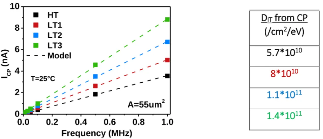
For quite some time, it was difficult to distinguish the impact of border and interface traps with the key point being the measurement speed. In the chase of border traps’ identification, we have some measurement methods as allies, like Charge Pumping, Low Frequency Noise and Time Dependent Defect Spectroscopy. Details for all of them will be presented in the next sections.
1.3 Bias Temperature Instability
Now that we have a general idea regarding the defects in the gate oxide, let’s discuss about how they affect the electrical parameters of MOSFETs, unfortunately always in a negative way: the widely known reliability.
Maybe the most recognized illustration among reliability engineers is the one in Figure 1.9, the bathtub curve. It indicates the lifecycle of an electronic component, or a transistor in our case, and is composed of three parts: the infant mortality, the useful life and the wearout. We all want to avoid the first one and stay as much as possible in the second one. Regarding the third part, we would all wish to never go there, but that’s not how it works! The infant mortality
21
is related to pre-existing defects and is correlated to the yield that we mentioned before. During the useful life, there are only some random defects in the transistor, now necessarily affecting it. Eventually, we arrive in the wearout part, caused usually by accelerated testing and characterization in extreme conditions of voltage, current or temperature. The questions that emerge in this part are: why, when and how this failure has occurred. In the case of the CMOS technology, specifically the Front End of the Line (FEOL) reliability, there are three degradation mechanisms: one that describes the sudden failure of transistors, called Time Dependent Dielectric Breakdown (TDDB) or the gradual one, as it is the case with the Bias Temperature Instability (BTI) and the Hot Carrier Injection (HCI).
In this section and, in general in this thesis, we will focus only on the second type of failure and specifically the BTI.
Figure 1.9 Bathtub curve showing the lifecycle of a product.
1.3.1 BTI degradation
The principle of BTI is to force a stress voltage on the gate by keeping, at the same time, the drain and the source at 0V as it appears in Figure 1.10. In that way, there is no drain current flowing in the channel and makes it possible to record the threshold voltage drift that occurs with time. Since it is an acceleration test, part of the wearout period, it is typically performed
at a high temperature of 125°C. When this method is implemented on NMOSFETs the VG stress
is positive (PBTI) which causes a negative oxide charge that leads to a positive VTH shift. The
opposite applies on PMOSFETs (NBTI): the VG, stress is negative which induces a positive oxide
trapping that results to a negative VTH shift (Figure 1.11). But this time, there is an additional
impact: the creation of interface states, as well, impacting the mobility, transconductance and subthreshold slope degradation. Historically, it’s the NBTI that constitutes the major reliability problem, since PMOSFETs are subjected to a degradation almost four times higher than the corresponding NMOS. For that reason, the research for a model suitable for NBTI prediction and description is of an imperative need.
Fai
lur
e
ra
te
Time
Infant
mortality
Useful
life
Wearout
22
Figure 1.10 FDSOI MOSFET under BTI stress.
Even though NBTI is a problem that is bothering the reliability community for more than 50 years, there are still some blank spots regarding its origin which, consequently, has emerged disputes for its modeling [53], [54]. Especially, with the CMOS advancement on oxides (high-k), process (i.e. nitridation) or structures (Trigate), it has become an important concern will trying to ensure the lifetime of a transistor. We’ll see now an overview of the existing models, separated in two different approaches, and the recent progress regarding the physical explanation of this reliability concern.
Figure 1.11 Typical VTH shift of stress and
recovery in FDSOI MOSFET.
1.3.2 Reaction-Diffusion model
The first attempted try, to describe the creation of interface traps during a NBTI stress was called Reaction-Diffusion (R-D) model [55], [56]. This model is based on the breaking of the Si-H bonds at the Si/SiO2, forming dangling bonds, and the diffusion of the charged hydrogen
atoms into the gate oxide. The free hydrogen can then recombine with other available atoms forming molecular H2 that can also diffuse into the gate oxide (Figure 1.12). Nonetheless,
several process knobs tend to improve this situation, like with the use of forming gas (H2) or
high-pressure deuterium anneal that seems to “cure” the dangling bonds which means that the NBTI degradation is mainly related to the interface states. This worked really well during that time, since everyone was mostly concerned about the kinetics of interface traps to explain the degradation. VG <0 VD=0 VS=0 Drain Source MG BOX Oxide 10-3 10-1 101 10 20 30 40 50 60 70 80 90 10-5 10-3 10-1 101 NBTI shift (mV)
Stress time (sec)
Vg,relax = 0V T=125°C Vg,stress = -2V T=125°C PMOS WTOP=60nm L=25nm
23
Figure 1.12 Reaction-Diffusion model principle.
But, the development of fast measuring techniques, over the past decade, has revealed the limitations of the model. Specifically, it has proven difficult for the R-D to fully describe experimental results [57], especially in the relaxation part [58], [59], [60]. The recovery part starts as soon as the stress is removed and it is globally uniform over the entire relaxation period. The R-D model could only predict a relaxation during 4 decades of time while the recovery should be relatively slow. In addition, the relaxation predicted by the R-D model is due to the back scattering of the neutral H2 species to the substrate. Since they are neutral, they
should not be influenced by the gate bias during relaxation, but experiments have shown that the relaxation is highly dependent on the applied VG, relax [60]. Finally, while the R-D model
predicts that the relaxation depends on the initial hydrogen concentration, it has been shown that is independent of the Si/SiO2 interface passivation [58], [61].
1.3.3 Huard’s model
It was not until 2006 that a new interpretation of the NBTI physical mechanisms appeared [61]–[63]. Huard this time considered two different components of NBTI degradation, independent from one another, the permanent and the recoverable. The recoverable part that is due to the hole trapping occurring mostly in pre-existing defects with long capture and emission time constants, which can be reversible since the holes can be re-emitted into the channel or the gate. This means that this part of degradation is exclusively related to the fabrication process of the device. On the other hand, the permanent part, attributed to the aforementioned dangling bonds created by stress. This time, we are talking about very fast defects with short time constants which are very difficult to be repassivated with the process steps that we saw before.
1.3.4 Grasser’s model
A few years later, in 2009 [64], Grasser proposed a different version of Huard’s model where the permanent and recoverable phenomena are related. The creation of interface states may be justified from the R-D model but not only, while it predicts the hole trapping taking place in stress-driven gaps. It is now called a quasi-permanent phenomenon since it can have long recovery times, longer than the experimental timescale. The recoverable part, at the same time, is considered to be explained by the capture of holes in oxygen deficiencies through Multi Phonon Field Assisted Tunneling. Even though this model, can reproduce experimental data of stress and relaxation, it faces some difficulties when it comes to other gate oxides or processing steps, since it cannot consider deficiencies other than the oxygen ones. This led to an update
Silicon Oxide Metal
Si Si Si Si Si Si Si H H H H H H H H2
24
of the existing model in 2014 [65], indicating that the recovery is more reaction-limited than diffusion-limited.
Right now, we are still considering two different components of the NBTI degradation, but there are some updates regarding the microscopic defects that are responsible for each one [66], [67]. For the hole trapping and the recoverable part, it is assumed that it is due to hydroxyl E’ center created by the attachment of the released atomic hydrogen to strained bridging oxygen centers. In the meantime, the quasi-permanent kinetics, of the interface states, are still following a power law dependence, but there is an extra consideration. Apart from the dangling
bonds in Si/SiO2 we may have hydrogen diffusing from the gate that could create additional
border traps. In both cases, the repassivation or redistribution of H is possible, but has very long recovery times.
In general, there are some parts of common agreement among the researchers, like the role of hole trapping/detrapping and the creation of defects during stress, but there is still no consensus and, most importantly, no predictive physical model that allows simulation under different circuit conditions [53].
1.4 Characterization of averaging effect
To identify and characterize the defects that cause the CMOS devices to degrade over time, we need some techniques to help us do that. In the next sections, we’ll see an overview of the used characterization methods in this thesis, starting with the ones that show the averaging effect of traps.
The first reliability characterization technique that has been used in this thesis, is the Bias Temperature Instability: a method to stress both N&PMOSFETs, called Positive (PBTI) and Negative (NBTI) respectively. The main ageing feature, as we saw before, is the shift of the threshold voltage with time while the transistor is on standby mode, there is no drain current flowing in the channel (VD=0V). It is an indicator of the gate oxide quality and helps towards the
optimization of the gate oxide or the channel material depending on the results each time. It can be applied in two forms: the DC and the AC that we’ll describe separately.
1.4.1 DC stress
The BTI application has two different stages, the stress and the relaxation. BTI is strongly activated by temperature and so it’s globally measured at 125°C. At the beginning of the technique, we perform an initial ID-VG to characterize the device and evaluate its VTH. During
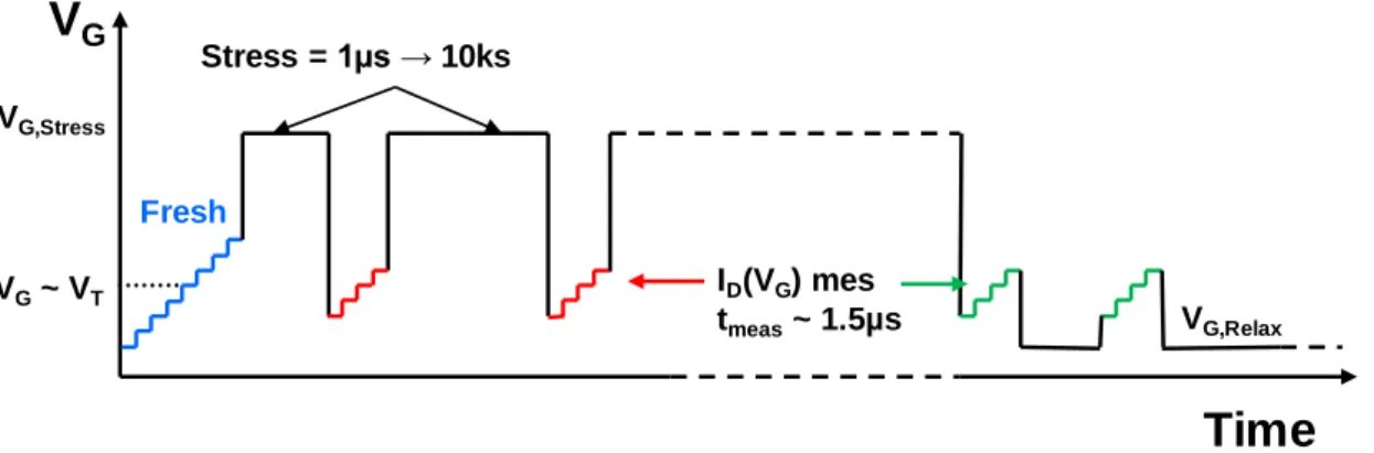
stress, a high gate voltage is applied for a specific time period, followed by the measurement itself during which we observe the degradation of the transistor’s parameters. The whole sequence is repeated several times over the total stress period, that’s why it is often referred to Stress-Measure-Stress (SMS) or Measure-Stress-Measure (MSM) in the literature (Figure 1.13). The only difference between NBTI/PBTI is the application of negative/positive VG, stress.
However, once the stress stops the degraded electrical characteristics tend to return in their original state, called relaxation.
25
Figure 1.13 Time chart of the applied gate voltage during an DC BTI stress.
Depending on the stress time, the degradation is not the same each time and since the recovery is quite strong, it is possible to overestimate/underestimate the reliability/degradation as it is evident in Figure 1.14. Due to that, it is suggested, if not imposed, to use a fast measurement methodology to limit the relaxation and along with a shorter measuring time after stress (fewer ID-VG points for example) we can have a clear aspect of the
actual degradation.
Figure 1.14 Impact of BTI relaxation in the final degradation level, reproduced from [68].
Figure 1.15 Threshold voltage drifts with time for different VG, stress during a fast range NBTI.
The difference between conventional and fast range methodology lies in the measuring tools. Typically, the VG, stress is applied through a System Measuring Unit (SMU) which,
unfortunately, has settling time in a millisecond range. So, in our case, it has been replaced by a Waveform Generator Fast Measuring Unit (WGFMU) connected to a Remote-sense and Switch Unit (RSU), placed in a B1530A Keysight module. An extra advantage is that we are able to watch the degradation for over 9 decades of time, from 1μs to 1ks (Figure 1.15). However, there is a trade-off between accuracy and speed. For a device with a large width (common in BTI measurements) we reach a current range of 100µA which means we can have an accuracy/speed of 1µs in our results. On the contrary, if we move to smaller gate width, like in
the case of nanowires (used in TDDS measurements in next section), we acquire an ID10µA
which forces us to measure with a speed of 100µs.
V
G VG,Stress ID(VG) mes tmeas~ 1.5µsTime
Stress = 1µs → 10ks VG~ VT Fresh VG,Relax Measuring time Effective degradation Apparent degradation Stress Stress StressUnderestimation of degradation
Time
ΔVT ΔV
Twith no relaxation
ΔVT with 0s waiting time
ΔVT with 15s waiting time
ΔVT with 45s waiting time
Incompressible time depending on the equipment
10-6 10-4 10-2 100 102 20 40 60 80 100 120 140 PMOS W=10m L=0.1m T=125°C 0.1% NBTI shift (mV) Stress time (s) VGstress= -1.4V -1.6V -1.8V -2V
26
As a result of the two aforementioned advantages, we are able to extract the real lifetime for our devices using this fast range methodology. The reliability criterion, in CMOS technology, is to establish a VTH shift of 50mV after a 5-year operation at the circuit operating voltage, so
for a VDD=0.945V in our technology (Figure 1.16). An extra consideration has to be the
variability, which is enhanced in advanced MOSFETs. Just like one transistor is not identical with another one, so is their reliability. NBTI shifts differ from one device to another due to the fluctuation of the number of traps per device. Consequently, the level of degradation is not the same, so the extrapolation is better to be made within a 3-sigma deviation (3σ) in order to include the variability and have rock evidence about the reliability each time. By measuring the ΔVTH through a range of VG, stress and scaling it to the supply voltage, it is possible to extract the
shift at 5 years lifetime and also the Time-To-Failure for the 50mV criterion (Figure 1.16 & Figure 1.17).
Figure 1.16 Log-log plot of Figure 1.15 scaled at VDD to extract the VTH shift after a 5-year
operation.
Figure 1.17 Demostration of successful technology validation, reaching and exceeding
the reliability criterion for a VG>0.9V.
Using the following power law model (Eq. 1.5), we can estimate the maximum applied voltage, in order not to pass the ΔVTH=50mV, and which has to be higher than the supply voltage
in order to validate each technology.
𝛥𝑉𝑇𝐻(𝑡, 𝑉𝐺, 𝑇) = 𝐶 ∙ 𝑉𝐺 𝛾
∙ 𝑒−𝑘𝑇𝐸𝑎 ∙ 𝑡𝑛
Eq. 1.5
where:
- C: a constant depending on the technology, specifically on the gate stack - T: the used temperature (125°C at BTI setups)
- VG: the stress voltage applied at the gate
- γ: the voltage acceleration factor
- Ea: the activation energy of the generated traps
- k: Boltzmann’s constant
- n: a time acceleration constant - t: the total stress time
As a result, and as we continue scaling and reducing the supply voltage even more, it is essential to measure the degradation as fast as possible, in order to correctly evaluate the
10-6 10-4 10-2 100 102 104 106 108 1010 1 10 100 1000 TTF@50mV =32.5y Scaled to V DD+5% PMOS W=10m L=0.1m T=125°C VT@5years =34.4mV NBTI shift @3 (mV) Stress time (s) -1.4V -1.6V -1.8V -2V 0.6 0.9 1.2 1.5 1.8 2.1 2.4 100 101 102 103 104 105 106 107 108 109 PASS if VG>0.9V TTF @3=99.9% VG@5y =1.01V PMOS W=10m L=0.1m T=125°C 5years TimeTo Failure@ V T =50mv (s) IVG stressI (V)
27
lifetime duration of the transistors and, eventually, of the circuits. In addition to the proper equipment, it is important to understand the physical mechanisms lying behind the measured degradation and build correctly calibrated models to help us predict the behavior of our devices during long operating times.
1.4.2 AC stress
Like the name indicates, there is an alternative way to apply BTI stress in a transistor, this time using the AC method. In that case, we better reproduce the circuit operation for which the stress voltage is not applied constantly. Like a circuit oscillates between 0V and the supply voltage VDD, the applied stress switches from 0V to VG, stress. Again, there is a series of stress and
relax events, called cycle, and the measuring principle is the same, a Measure-Stress-Measure sequence, recording the ID-VG characteristic to extract the VTH shift, similar to the DC BTI (Figure
1.18).
Figure 1.18 Time chart of the applied gate voltage during an AC BTI stress with the inset showing a single period of it, taken from [69].
Using the AC technique, we have to identify two parameters: the frequency and the Duty Factor (DF), described by:
𝑓 =1
𝑇 Eq. 1.6
𝐷𝐹 = 𝑇𝑠𝑡𝑟𝑒𝑠𝑠
𝑇𝑠𝑡𝑟𝑒𝑠𝑠+ 𝑇𝑟𝑒𝑙𝑎𝑥∙ 100% Eq. 1.7
The frequency is describing the operation speed of the circuit while the duty factor reveals the percentage of the period that the circuit is “on”. For example, during a 10% AC BTI application, the transistor is stress during 10% of the defined period and the rest 90% is under relaxation. We can perform tests from a duty cycle of 1% up to 100% (Figure 1.19), with the maximum percentage being the DC BTI that we saw before, and over a wide range of frequencies from 100Hz up to 1MHz. Each time the AC degradation will be lower than the DC one. This is due to the fact that the end of AC signal has a 0V state which means relaxation. So again in this type of measurement, it is necessary to have a fast range setup to avoid any
VG VG,Stress ID(VG) mes. tmes~ 1.5µs VG~ VT Initial VG,Relax Stress BTI AC VG=0V 1 AC Stress Period Vg t T=1/f TStress TRelax Time
28
relaxation phenomena. In our case, we have used a previously developed fast methodology, operating under the “Arbitrary VG Pattern” (AVGP) method, described in details in [70].
The best way to exploit AC BTI data, is to build the Capture and Emission Time (CET) maps [71] (Figure 1.20). Using this method, we can identify two trap populations, the permanent and the recoverable. The first one has a very high emission time compared to the capture ones and is related to the interface traps while the latter experiences a strong correlation between capture and emission and is mostly due to the traps deeper in the oxide.
Figure 1.19 . Illustration of a PMOSFET VTH
degradation under DC and AC stress conditions.
Figure 1.20 CET map revealing the two populations according to their time constants
[70].
Of course, the next step is to have a model that is able to describe the experimental results and predict the degradation for AC and AVGP stress. The model that has been used to reproduce the VTH shift in combination with the CET maps, is the RC model [70], [72] (Eq. 1.8).
∆𝑉𝑇𝐻(𝑡) = 𝐾 ∙ ∑ 𝑔(𝜏𝑐𝑖, 𝜏
𝑒𝑖) ∙ 𝑈𝑖(𝑡) 𝑁
𝑖=1
Eq. 1.8
where K is a technological constant, g(τc, τe) the local density of capture and emission time
constants and U the voltage after n stress cycles: all of them individual parameters for each “i” trap. In this model, each trap can be seen as a lumped RC element with given resistance and capacitance. Taking the local trap density extracted from Figure 1.20, we are able to successfully fit our data, like the ΔVTH recovery for different AC stress periods, the normalized
stress and recovery for different frequencies or w.r.t. the duty factor. 1.5 Characterization of individual defects
Besides the characterization methods used for large devices to record the averaging effect of traps, as we move on to deeply scaled devices, we are witnessing the impact of only a handful of random defects. For that, it becomes imperative to have reliable techniques to characterize the individual traps.
VT shift ( a.u .) Time (s) DC=100% DC=70% DC=50% DC=30% ‘Quasi-permanent’ traps
29
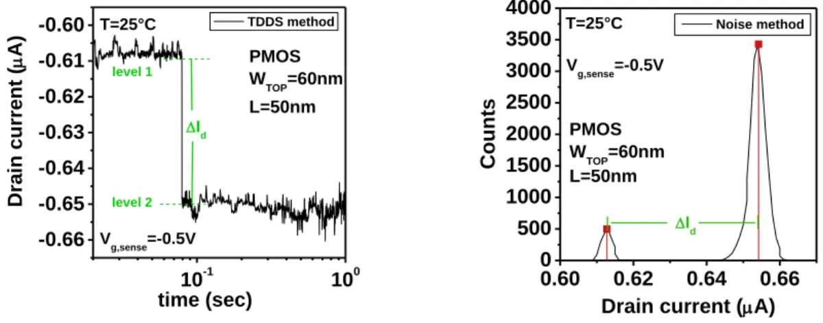
1.5.1 Random Telegraph Noise – Low Frequency Noise (stationary method)
One of the first applied techniques for trap detection method is the Random Telegraph Noise (RTN), a method suitable for small gate areas. When a trap inside the oxide randomly captures and emits a carrier from the conduction channel, it causes a fluctuation of the electrical parameters of the transistor, especially in the drain current. This appears like discrete switching between two current levels in the time domain. Two current levels correspond to one trap, four levels to two traps etc. Each trap has three specific characteristics that make it unique: the capture time constant τc, the emission time constant τe and the drain current
variation ΔID that eventually has an impact on the threshold voltage. These type of fluctuations
have been observed for quite some time and are evident in devices with surface smaller than 0.1μm2 [73], [43], where it is easier to be detected due to the smaller existing number of traps.
Figure 1.21 RTN of a FDSOI PMOSFET transistor during a VG, bias of -0.5V.
Figure 1.22 Impact of a single trap in the drain current
The usually applied gate voltage is part of the subthreshold region. Figure 1.22 shows the reason for this choice. Applying different gate bias on a MOSFET, we can identify two different zones of the trap. The left part in which the impact on the drain current reaches a maximum and constant value and the right part during which this effect decreases with the increasing operating drain current. The decrease in the strong inversion regime results from the screening of the oxide layer by mobile carriers of the inversion layer [43]. It is therefore related to the current flowing across the transistors through the equation [74]:
∆𝐼𝐷 𝐼𝐷 = 𝐺𝑚 𝐼𝐷 ∙ 𝑞 𝑊 ∙ 𝐿 ∙ 𝐶𝑂𝑋 Eq. 1.9
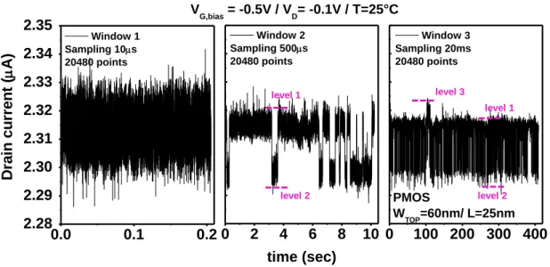
During the bias application, we keep the device in quasi-thermal equilibrium and we see the multiple captures and emission of the same defect. This means that we can see and detect only a small portion of the existing oxide traps, depending on the setup each time, like the bias conditions and the experimental measuring window. Figure 1.23 shows the current transients of the same PMOSFET, having a constant sampling time, but a different applied gate voltage. It
6.0 6.5 7.0 7.5 8.0 2.28 2.29 2.30 2.31 2.32 2.33 Drain current ( A) time (sec) Filled trap Empty trap 10-9 10-8 10-7 10-6 10-5 10-4 0 5 10 15 20 25 30 35 40 Subthreshold regime I D /ID0 from a sin gle charge (%) ID0 (A) Strong inversion W TOP=60nm L=25nm
30
is obvious that the number of detected traps is directly related to the applied VG and such, we
can see from zero up to two current fluctuations.
Figure 1.23 Current fluctuations of one transistor under different bias application.
Besides the voltage, it is also the experimental window that affects our results. In Figure 1.24, it is evident that the sampling rate plays an important role in the measurements. We can see that, under a fixed pair of (VG, VD) there are some differences: in the first “window”, there
is no discrete switching visible while one the second and the third one, there are two and even four witnessed current levels, meaning that we have slower traps. In addition to that, the need of a large number of points [75], like here the selected 20.480, makes it more complicated to analyze the data after, especially when it comes to the determination of their characteristic capture and emission times.
Figure 1.24 Three experimental measuring windows with different sampling rates showing the complexity of RTN method for trap detection.
-0.423 -0.420 -0.417 -0.705 -0.700 -0.695 0.0 0.1 0.2 0.3 0.4 0.5 0.6 0.7 0.8 -2.98 -2.97 -2.96 -2.95 VG = -0.38V VG = -0.42V Dra in current
(
A)
time (sec) VG = -0.6V 0.0 0.1 0.2 2.28 2.29 2.30 2.31 2.32 2.33 2.34 2.35 0 2 4 6 8 10 0 100 200 300 400 D ra in c u rr e n t ( A) Window 1 Sampling 10s 20480 points V G,bias = -0.5V / VD= -0.1V / T=25°C time (sec) Window 2 Sampling 500s 20480 points PMOS W TOP=60nm/ L=25nm Window 3 Sampling 20ms 20480 points level 1 level 2 level 1 level 2 level 331
A relatively easier way to exploit the RTN data is to construct the drain current histograms (Figure 1.25) [76]. Even with a first glance, we can be more confident on the current fluctuations that have been measured and the existence (or not) of a defect. If we observe window 1, we see that the current is drifting around a specific level; one that is directly illustrated on the left histogram (2.31µA). On the contrary, in the two other windows/histograms, there are two or even three different ID levels, showing a series of capture/emission events that correspond to
one or two traps respectively.
Figure 1.25 Respective drain current histograms of Figure 1.24.
Now, we also have the option to switch from the time domain to the frequency domain and use the Low Frequency Noise as a diagnostic approach for the detection of defects. To do so, we take the raw data of ID-t and use Welch’s method [77] to make this transformation resulting
to use the Power Spectral Density (PSD [A2/Hz]) as a tool.
The method is based on the following concept: The original time signal is split in 1024 overlapping subparts, in our case, defining like this the averaging in the calculating periodograms, an important factor that reduces the variance of the individual power spectral results. Then, these overlapping segments have a window applied to them, in the time domain: we selected the Hanning window which is most commonly used in noise analysis due to its good frequency resolution.
After, we take the difference between the timestamps:
∆𝑇 = 𝑡2− 𝑡1 1.10 Eq.
and calculate the minimum and the maximum frequency of our segment using the previously mentioned number of points per window (here 1024):
𝑓𝑚𝑖𝑛 = 1 ∆𝑇 ∙ 1024 Eq. 1.11 2.28 2.31 2.34 0 500 1000 1500 2000 2500 3000 2.28 2.30 2.32 2.29 2.30 2.31 2.32 2.33 Cou nts Window 1 Sampling 10s 20480 points VG,bias = -0.5V / VD= -0.1V / T=25°C Drain current (A) Window 2 Sampling 500s 20480 points PMOS W TOP=60nm L=25nm Window 3 Sampling 20ms 20480 points level 2 level 1 level 2 level 1 level 3 level 1 ΔI D ΔID1 ΔID2
32 𝑓𝑚𝑎𝑥 = 1 ∆𝑇 Eq. 1.12
continuing with their difference, which will serve as our sampling frequency in the PSD:
∆𝑓 =𝑓𝑚𝑎𝑥 − 𝑓𝑚𝑖𝑛
1024
Eq. 1.13
The corresponding periodogram (PSD) is calculated for each window using Fast Fourier Transform (FFT) and finally, we average the calculated periodograms, with the previous value.
𝑃𝑆𝐷 =𝐹𝐹𝑇
2
∆𝑓
Eq. 1.14
The PSD shape of RTN has a 1/f2 dependence, called Lorentzian and as we scale down we
experience a strong noise dispersion (Figure 1.26). The PSD is described by [78]:
𝑆𝐼𝐷 = 4 ∙ 𝐴 ∙ ∆𝐼𝐷2 ∙ 𝜏
1 + (2𝜋𝑓)2𝜏2
Eq. 1.15
where ΔID is the average RTN amplitude (Eq. 1.9), τ is the time constant of transitions given
by: 𝜏 = (1 𝜏𝑐 + 1 𝜏𝑒) −1 Eq. 1.16
with τc and τe, the capture and emission time, respectively and A the space mark ratio
described by:
𝐴 = ( 𝜏
𝜏𝑐 + 𝜏𝑒)
Eq. 1.17
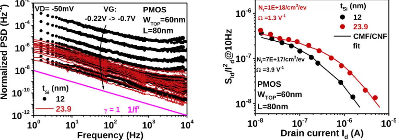
This method can be applied on both large and small area devices with the difference lying on the shape of PSD. On larger transistors, there is an increased number of traps, each one with a distinguished Lorentzian spectrum. As they are averaging, the new spectrum will fit the 1/fγ
form, the so-called flicker noise (Figure 1.27). Depending on the γ value, we can identify the position of the traps in the oxide (0.7< γ <1.3) [79]. For a value lower than 1 the traps are located near the interface while when the value is higher than 1 the traps are positioned deeper in the oxide. If γ=1, then we have a uniform trap distribution near the interface.