THE DESIGN AND REALIZATION OF HIGHER ORDER VARACTOR FREQUENCY MULTIPLIERS
by
JOSEPH FRANCIS BALCEWICZ
S. B., Massachusetts Institute of Technology 1966
SUBMITTED IN PARTIAL FULFILLMENT OF THE REQUIREMENTS FOR THE DEGREE OF
MASTER OF SCIENCE at the
MASSACHUSETTS INSTITUTE OF TECHNOLOGY June, 1967
Signature of Author L
-Department of Etr c l ngineer May 25, 67
Certified by - .-.. - - -. ==
Thesis Su rvisor
Accepted by ---- ---. ::=.::--...
THE DESIGN AND REALIZATION OF HIGHER ORDER VARACTOR F2IEQUENCY MIJLTIPLIERS
by
JOSEPH FRANCIS BALCEWICZ
Submitted to the Department of Electrical Engineering on May 25, 1967 in partial fulfillment of the require-ments for the degree of Master of Science.
ABSTRACT
A solid-state UHF signal source is quite. desirable from the
point of view of low power consumption and noise. It has been proposed to frequency multiply an existing VHF source into the
UHF range by using a high order varactor multiplier. A 249.1 lvhz
source is available and realizable varactor sextupler will be designed to provide a low S-band source at 1494.6 IMihz.
The varactor diode, under the condition of reverse bias,
exhibits a non-linear junction capacitance. This effect generates a series of harmonics of the drive frequency. Thus, the problem in designing a frequency multiplier is to find some sort of im-bedding network that will match the diode's impedance values dt
the harmonics we wish to be present. The impedance specifications -for this network have been previously determined so this thesis is
involved in discovering a method of physically realizing the im-bedding network.
The impedance specifications depend strongly on the maximum value of the junction elastance. A procedure for measuring this
value as well as such diode parameters as the series resistance and reverse breakdown voltage has been described and the msults presented for a sample of Motorola varactor diodes.
A low-pass input filter was designed for the multiplier to
prevent any unwanted excitations of the diode. A band-pass out-put filter, centered about the sixth harmonic, was also designed to prevent any spurious responses in the output of the multiplier.
Two possible realizations of the imbedding network are de-rived. One, the shorted stub structure, is analogous to the low frequency realizations of varactor multipliers. The other, a transformer structure, is a single unit which matches the proper
impedance levels.
A major feature of this research is in the use of a computer
versus space charge layer stored charge characteristics were derived by computer analysis of capacitance versus reverse volt-age data.
In addition, the design of the low-pass input filter and the transformer imbedding network was done on a computer. The input filter was constructed and a comparison is made between the pre-dicted and actual characteristics of this filter.
Thesis Supervisor: Robert P. Rafuse
ACKNOWLEDGEIMENTS
I would like to express my deep appreciation to Doctor Robert P. Rafuse for agreeing to supervise this thesis and for his constant interest in the results determined. I would also like to thank Donald H. Steinbrecher for the many ideas and contributions he has made to this research.
TABLE OF CONTENTS
Title Page ... 1
Abstract
...
2Acknowledgements ... 4
Table of Contents ... 5
List of Figure Captions ... 6
List of Table Titles ... ... 8
Chapter 0 - A Preliminary Discussion ... 9
Section 0.1 - Introduction ... 9
Section 0.2 - The Step-Recovery Diode ... 9
Section 0.3 - The Synthesis of a Realizable Multiplier...13
Chapter I - Determining the Diode Parameters ... 17
Section 1.1 - Introduction ... 17
Section 1.2 - The M4easurement of R ... 18
Section 1.3 - The Measurement of C(V) and VB ... 22
Chapter II - The Input and Output Filters ... 26
Section 2.1 - Introduction ... ... 26
Section 2.2 - The Output Filter ... 27
Section 2.3 - Computer-Aided-Design of the Input Filter ... 31
Section 2.4 - The Performance of the Input Filter ... 37
Chapter III - Design of the Imbedding Network ... 41
Section 3.1 - Introduction ...
41
Section 3.2 - The Shorted Stub Method ... 41
Section 3.3 - Computer-Aided-Design of the Transformer Imbedding Structure ... 50
Chapter IV - A Summary of Important Results and Conclusions ... 54
Section 4.1 - Summary ... 54
Section 4.2 - Suggestions for Additional Investigations ... 55
LIST OF FIGURE CAPTIONS Figure 0.1: Figure 0.2: Figure 0.3: Figure 1.1: Figure 1.2: Figure 2.1: Figure 2.2: Figure 2.3: Figure 2.4: Figure 2.5: Figure 2.6: Figure 2.7: Figure 3.1: Figure 3.2: Figure 3.3: Figure 3.4:
Junction Elastance Versus Stored Charge - Motorola Type MV 1805-C Diode.
Model for a Reverse Biased Step-Recovery Varactor Diode. -Junction Capacitance is.a Non-Linear
Func-tion of the Reverse Bias Voltage.
Schematic, Diagram of a Varactor Frequency Sextupler. Z((j ) is Specified in Equations 0.2.
Schematic Diagram of R Measurement Test Jig.
Schematic Diagram of Test Setup for C(V) Measurements. Inter-Digital Band-Pass Filter - Center Frequency
1494.6 Mhz; Mid-Band Loss < 1.0 db.
Attenuation Characteristic of the Output Filter. Finger-to-Ground Wall Spacing = .194".
Low-Pass Filter - Cut-Away View of Low Impedance Elements. Pass Band Edge at 360 Mhz. Pass Band Attenuation: Less than .5 db.
Computer Analysis of Input Filter Design - L(5)=1.82. Computer Analysis of Input Filter Design - L(5)=1.85. Computer Analysis of Input Filter Design - L(5)=1.87. Asymptotic Behavior of Input Filter Attenuation
Characteristic.
The Shorted-Stub Approach to Realizing the Required Imbedding Network. There is a Stub for the Input, Output and Each Intermediate Frequency.
The Transformer Approach to Realizing the Required Imbedding Network.
Impedance Versus Frequency for Shorted Stub, Z (&) ),
and Tuning Capacitor, Zc (W ). Zs + Z = Z . At
C) = 2w0 ,Z = j9.55 ohms.
Physical Realization of the Shorted Stub - Tuning
Figure 3.5: Bias Scheme for Diode in Shorted Stub Realization of Imbedding Network.
Figure 3.6: Computer Analysis of Transformer Imbedding Network. Figure 3.7:- Impedance of an L - C Parallel Combination Versus
Frequency.
Figure 4.1: Schematic Diagram of a Universal Frequency Quin-tupler Utilizing Shorted-Stub Approach.
LIST OF TABLE TITLES
Table 1.1: A Summary of R Values
Table 1.2: A Summary of Cmin' Smax and V Values
Table 2.1:
Table 3.1:
Comparison of Predicted and Actual Low-Pass Filter Characteristics
A Summary of the Shorted Stub Imbedding Network Design Parameters
Table 3.2: A Summary of Impedance Values Pertaining to the Transformer Structure Design
CHAPTER 0
A PRELIMINARY DISCUSSION
Section 0.1 - Introduction
There has been much controversy lately about the use of varactor, step-recovery, diodes for frequency multiplication in the UHF and microwave ranges. It would be very useful to be able to develope a highly efficient microwave frequency multiplier, for this step would ultimately yield a high power microwave signal
source. Multiplying an existing solid-state VHF source into the microwave spectrum by an efficient method such as the varactor multiplier would produce a completely solid-state (and thus
effi-cient) source of microwave energy.
In the present case, a crystal controlled, phase-locked source at a frequency of 249.1 Mhz is available and a realizable varactor sextupler will be designed to multiply this input frequency up to 1494.6 Mhz (low S-band).
Section 0.2 - The Step-Recovery Diode
A step-recovery diode is one in which the junction capacitance as a function of the reverse bias voltage has a well defined mini-mum value (or the elastance has a maximini-mum value). Figure 0.1
shows a typical graph of a step-recovery diode's elastance under reverse bias. The details of how thesemeasurements were carried out are given in Chapter I..
The model that will be used for the diode under the reverse bias condition is given in Figure 0.2.C(V) is the junction
capa-citance and Rs is the bulk series resistance of the diode. It is assumed to be constant for all values of reverse bias. The details of how the measurement of Rs was carried out is also given in
Chapter I.
The theory of varactor frequency multiplication was presented in a book by Paul Penfield, Jr. and Robert P. Rafuse entitled
Varactor Applications,. (M. I. T. Press - 1962). In it, the effi-ciency of a 1-2-3-6 and a 1-2-4-6 varactor sextupler was derived.
0.05--0.04 0.03
0.0?
0.01--200 400 ,00 800 1000 /200 1400 1600 1800 (PIcoCOLUMBS) STOREDCH ARG E
F\GURE
CARGE
0.
ELST NGO
V EWSUiS
STORE
D
-
NOTOROLN TYPE
M\
\05~-C
I
RS
~~QU+
0V2
M\ODEL
FOR~ A~
R
VRSE
'RECI0VERY
\/ARNOT0)?\ '\ODS.
OCkFAU
TANCE
GE'ThE REVERSE\0LAE
)
5-TEP-T
U
NCT ON
vUNCTnON
ON4
S A NCN-LNF R
'B KS \1 OETAG-E 0
(The former configuration implies idlers at the second and third harmonics and the latter implies idlers at the second and fourth harmonics). The efficiency is given in terms of the diode's cut-off frequency, fc, which is given below in eq. 0.1,
-.. (0.1)
where Smr and Smin are the maximum and minimum values of junction elastance respectively.
For a typical diode measured(see Fig. 0.1) Smax is approxi-mately 6 X 10 10 darafs and S is approximately 0. Rs for a
typical diode is around .15 ohms so we can calculate a cut-off frequency of about fc =.63.6 Ghz. Thus, an input frequency of 249.1 Mhz is 3.9 X 10⁻³ X fc. Using Figures 8.46 and 8.50 given in Varactor Applications, the maximum predicted efficiency for a 1-2-3-6 sextupler is 62% and for the 1-2-4-6 sextupler is 69%.
Futhermore, it is felt that if idlers are included at each intermediate frequency, then a still greater efficiency will be possible. So, with this assumption, a 1-2-3-4-5-6 sextupler will be designed.
An interesting side note is some results published in July 1965 in -hp associates- Application Note #8, entitled, "Frequency Multiplication with the Step Recovery Diode". In it is presented
a graph of the predicted efficiency of a frequency multiplier operated at an input frequency of 100 Mhz and using the rectifi-cation characteristics of a forward biased diode instead of the non-linear capacitance characteristic of the reverse biased varactor. The diode used in their multiplier was an -hpa- 0241
step-recovery diode with a 0min = 3.3 pf, an Rs = .3 ohms and a cut-off frequency of 160 Ghz.
Their expected efficiency for a sextupler is approximately 59% while the same diode, operated under reverse bias in a 1-2-4-6 configuration would yield (according to Penfield and Rafuse) a 94% efficiency. This extra efficiency, amounting to an extra 2db
a realizable reverse biased, varactor sextupler.
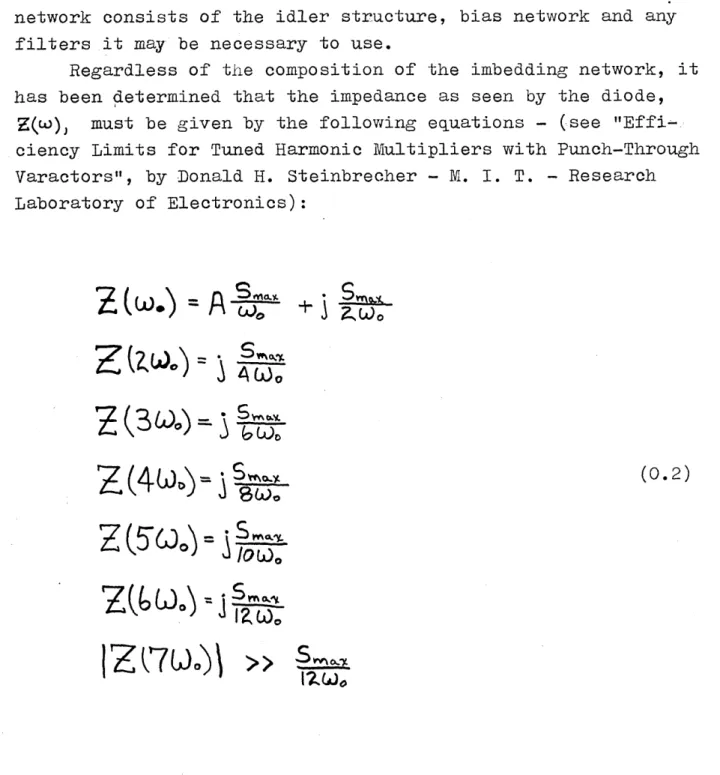
Section 0.3 - The Synthesis of a Realizable Multiplier
Figure 0.3 is a shematic representation of the frequency multiplier. In this case, if ), is the input frequency then a frequency of 6, is delivered to the load. The imbedding network consists of the idler structure, bias network and any
filters it may be necessary to use.
Regardless of the composition of the imbedding network, it has been determined that the impedance as seen by the diode,
Z(w), must be given by the following equations - (see
"Effi-ciency Limits for Tuned Harmonic Multipliers with Punch-Through
Varactors", by Donald H. Steinbrecher - M. I. T. - Research
Laboratory of Electronics):
WOW
(0.2)
S.S
INPUT
AT
(46
ki
OUTPUT
AT
6t J, LOADF\GURE O.3'
SCHEMATIC
DIAGRNAM
OF A VARCTOR
FREQUENCN'
5PEC\FIED
SEXTUPLER.
ZtL)
I*
SzQ(9 WO)
where A = 0.337 and B = 0.083. darafs and (o = 2 1T X 249.1 X Using a value of l06/sec = 1.57 X Smax = 109/se 6 X 10¹⁰ c we have the following impedance valuesZ()=
27
'Z7.
W
9.5
(in ohms).+ (\9.1
V)
Z(3o)
=
6.37)
rZ (4
.)
=
(4. r78)
Z(57Wo
(3.-Z
(0.3)Z(bo.)
=
3.
16
\Z(7w
.\
0
z WO)
\Z(80.O\
SMO'1. 14W
0va w
'-
O
0
')
(0.2)3
(3.18)
The values given in equations 0.3 are to be synthesized by two different-means. The first method bears a close 'resemblance to the low frequency synthesis of varactor multipliers. Essen-tially the diode is connected to a circuit which resonates at a specific intermediate idler frequency and thus eliminates this frequency from the output of the multiplier. In the low frequency design, these idlers take the form of either series or parallel L-C cirduits. In the UHF design, these idlers may be realized by the~use of shorted lenghts of coax with a suitable tuning capacitor. This method of realizing the idler network is dis-cussed in Chapter III.
Another and more aesthetically pleasing method of realizing the required impedance values is to use some sort of transformer structure (shown in Figure 3.2). The analysis of this type of structure is carried out on a computer and a suitable design can be found.
The compactness of this latter structure is its major fea-ture as far as constructing a working model goes.
In addition, the method of computerwraided-design for micro-wave circuits that was used for determining the parameters of this structure and also the parameters for the low-pass input filter may prove to be a valuable method of designing microwave circuits. It is very difficult to "breadboard" a microwave circuit as one would a lumped element circuit and so the use of a computer may prove quite useful for the design and optimization of UHF and microwave circuitry.
CHAPTER I
DETERMINING THE DIODE PARAMETERS
Section 1.1 - Introduction
It is important to be able to measure the diode parameters. Both Rs and C'(V), the circuit elements comprising the reverse bias model for the diode (Fig. 0.2), must be determined as well as such parameters as the breakdown voltage, VB , and the contact potential, 0. VB and
#
are defined here in the same way as in the literatureconcerning low frequency P-N junction devices.V is the reverse voltage at which avalanche multiplication occurs and thus the reverse voltage cannot exceed this value. # is the voltage that exists across the P-N junction when the diode has no applied voltage across it.
The necessity for knowing C(V) lies in the fact that the
minimum value of C(V) appears in eqi. 0.2, the required impedance of the imbedding network, (Smax = C mi). Thus, the imbedding struc-ture that is designed must be designed for a specific diode with a
specific Smax'
Rs ,VB and 0 are necessary because these values, in some sense, determine the maximum power handling capability of a diode and
therefore, of a frequency multiplier. The "normalization power", Pnorm, for a diode is given in equation 1.1 below,
(1.1) The greater Pnorm, the greater is the power that a varactor multi-plier can inherently handle.
For a typical case, let VB = 100 volts,
#
= .4 volts and R5-1 ohms. This yields a Pnorm of about 104 watts demonstrating that we may expect large power outputs (around 10-3 X Pnorm) from these' varactor frequency multipliers. It can also be seen from this
break-down voltage so # will be ignored in the following discussions. This chapter will be involved with describing the methods used to measure the remaining parameters and with presenting the results of these measurements.
Section 1.2 - The Measurement of Rs
The series resistance in the reverse bias diode model (Fig.0.2) is assumed to be constant for all frequencies and all power levels. In the actual diode, Rs results from the bulk resistance of the semiconductor material used to make diode. The measurements will be made on eight Motorola MV 1805 - C varactor diodes at a frequency of 500 Mhz.
Figure 1.1 is a schematic diagram of the, test jig used in the Rs measurement. It essentially consists of a half-wavelength long,
(11.8 inches), section of 15 ohm, rigid, coaxial transmission line. At the quater-wavelength point, there is a perpendicular tuning
stub with the diode imbedded in the inner conductor of the stub. Tuning of the stub, is accomplished by inserting a certain amount of dielectric material in the space between the stub's inner and
outer conductors. This varies the characteristic impedance of a part of the stub and allows the stub to be tuned.
The bias scheme for the diode consists of a hole with a spring in it. The spring, which is self-resonant at 500 Mhz, makes elec-trical contact with the diode and thus provides a certain amount of reverse bias.
The half-wavelength long line is driven at one end by a 500 N7liz source and the power transmitted through the line is read at the other end on a power meter. First the transmitted power with no tuning stub is read and then the transmitted power with the diode and tuning stub in place is read. The difference between these two values for transmitted power is a measure of R. plus any other
losses in the tuning stub. These additional tuning stub looses may be determined by using a solid brass "diode" (Rs = 0) and measuring the change in transmitted power. In this case, since there is no diode resistance, the difference in transmitted power is due to the stub's losses.
INPuT 15fL UNE -BIA5 (v'A RESo;NATING)
7I
DIODE TUNING STUB POW E R METER D\ELECTR\CFIGURE
SCNEMAT\C
'MEASUREMENT
irRAMOF
R9
TE5T
JTG-.
1.1
soo
Mal S\GN ALIf the ratio of power transmitted without the stub to power transmitted with the diode and the stub (in db) is G, then
G
= 10 lopj o()
(1.2)
In a low frequency model of this situation,
and 71 'RomaC'J
R
Coo. )RA
v4*17"' (1.3) Where R load is the load resistance seen at the quarter-wave point,Vwithout is the voltage across the load without the diode and stub and Vwith is the voltage across the load with the diode and stub.
Let
L
-% (1.4)then, by substituting this back into equation 1.2 we have:
G~IO
(1.5)
Furthermore, in. the low frequency analogy, Rload is the power meter's input impedance transformed back a quater-wavelength. So, if a 100 ohm thermistor mount is used, then
,o
=
(1.6)
Also, the maximum value of impedance for the diode-tuning. stub combination, when the imaginary part of the impedance is tuned out, is just , where R is the losses due to the tuning stub, (R + R 4.. Z0 , the characteristic impedance of the stub, equal to 5.7 ohms).
Now, using a voltage divider relationship, we have for L:
R1d
orSolving now for Rs:
R
;;
14.A
R
(1.8)
If the brass "diode" is used to find Rt, then: G = 29 db,
L = 28.1, (from eq. 1.5)
and Rt= .533 ohms, (from eq 1.8 with Rs = 0).
So finally, the equation for Rs is:
R= 14.4 - .533 ohms s L-1
This method was then applied to with the results summarized in Table
Table 1.1 - A Summary of Rs values Diode Number 1 2 3 4 5 6 7 8 18.1 db 19.5 db 22.0 db 24.4 db 20.2 db 21.0 db 19.0 db 19.2 db L 8.04 9.44 12.6 16.6. 10.2 11.2 8.92 9.12
the eight Motorola diodes 1.1. Rs (in ohms) 1.517 1.177 .708 .370 1.033 .879 1.285 1.242
It should be noted that the d.c. series resistance is be-tween 11 and 13 ohms for these varactor diodes.
This method then, is a straight-forward way to determine
the bulk a.c. series resistance of a varactor diode at a frequency of 500 Mhz.
Section 1.3 - The Measurement of C(V) and VB
The capacitance that exists across the junction of the varactor diodes is of prime importance since it determines the impedance
values that the diode must see if it is to be matched in the sex-tupler that will be designed.
Basically, the C(V) measurement is done on a Boonton Capaci-tance Bridge. An external D.C. bias voltage is fed into the Bridge and this produces the required reverse bias condition for the diode.
SIAS TEST SIGNAL
FIGURE
MCANI8TQR
12
SCEN
AT
IC
FOR
C()
DIAGR AM OF
TEST
5ETOP
MEA5URE MENT S.
B0o-T
ONCAPACITANCE
BRIDGE
The value of diode capacitance (which also includes the capac-itance of the casing and the leads) is read from the Bridge for various value of reverse bias voltage from 0 to the breakdown
volt-age. These measurements were made on the eight Motorola diodes at a frequency of 1 Mhz. Figure 1.2 is a block diagram of the test
setup.
After the capacitance values were taken for a specific diode, they were fed into the computer and a program known as L0'ADGO INTEG would calulate the elastance values (equal to the reciprocal of the capacitance values) and numerically integrate the capacitance-volt-age function to obtain a value for the charge stored in the
space-charge layer of the diode.
The equation relating a change in stored charge to a change in capacitance and voltage is:
dQ
=C(\V)
(1.11)
remember that C is not constant. So the charge, Q0, at some value of reverse bias boltage, V0, is given by:
(1.12)
and it is this integral that the computer evaluates. The data for the elastance versus stored charge plot (Fig. 0.1) was obtained
from the print-out for one of these diodes.
The reverse breakdown voltage may be determined in one of two ways. First, when the values of C(V) are being taken, it can be observed that there is a point where the bias voltage remains rela-tively constant and that an appreciable amount of reverse current
(greater than the saturation current) begins to flow. This value of reverse bias voltage is VE.
oscilloscope. The value of V3 method may be preferable since is.
Table 1.2 is a summary of age measurements made.
Table 1.2 - A Summary of C min'
Diode Number C (pf)
will be clearly visible. This it shows how steep the breakdown
the capacitance and breakdown
volt-S max and V Values
Smax (X 1010 darafs) VB 5.75 5.10 4.85 4.51 5.75 5.72 5.75 5.92 93.2 volts greater than 105 volts 89.6 volts 83.7 volts 101.6 volts 93.2 volts greater than 110 volts greater than 110 volts
By this method, the values of Smax were determined for. the samples of Motorola diodes. From these values, the specifications for an imbedding network can be determined.
This chapter has described general procedures by which the varactor diode parameters R,, C(V) and V may be measured. With
only a few modifications these procedure.s may he applied to varac-tors of various shapes and sizes. The use of the computer to nu-merically integrate the capacitance-voltage function made it quite
easy to obtain elastance and voltage versus stored charge data.
1 2 3 4 5 6 7 8 17.4 19.6 20.6 22.2 17.4 17.5 17.4 16.9
CHAPTER II
THE INPUT AND OUTPUT FILTERS
Section 2.1 - Introduction
Referring back to the schematic diagram of the frequency multiplier shown in Figure 0.3, we observed that the imbedding network would contain the impedance matching structure for the diode as well as the bias network and any filters it may be nec-essary to include. It is these filters toward which we now
direct our attention.
The need for filters comes from the fact that it may not be possible to completely eliminate all the other harmonics in the impedance matching network. An output filter is needed to insure that only the desired harmonic frequency is present in the output. and an input filter is needed to block any unwanted inputs into the multiplier. Thus, these filters serve to improve the noise figure of the entire multiplier.
The output filter is of the interdigital type. It is a band-pass filter centered around the sixth harmonic (1494.6 Mihz). It was designed for a 17% fractional 3 db band width and passband ripple attenuation of less than .2 db. The attenuation at Tu, and 7W0 was to be at least 60 db with no spurious passbands thru the twelfth harmonic.
The input filter consists of alternate lengths of high and low impedance transmission line. This is a field theory analogy to the low frequency low-pass filters consisting of series induc-tance and shunt capaciinduc-tance elements. The 3 db passband edge was set at 300 Mhz and a .2 db ripple was to be allowed in the passband. There would -be 60 db of attenuation at the second harmonic, 498.2hz. It was hoped that there would be no spurious passbands in the atten-uation characteristic.
The remainder of this chapter will present the design of these two filters as well as the predicted and actual responses of these filters.
Section 2.2 - The Output Filter
The design of microwave filters is a fairly routine process since there are many books and articles that detail the design considerations and list the filter parameters and how to choose them. One such book, a very complete treatment, is LMicrowave Filters, Impedance- - Matching Networks, and Coupling Structures
by GeorgeNL. Matthaei, Leo Young and E. M. T. Jones, published
by Mc Graw - Hill - 1964.
The band-pass, output filter design was taken from this book. The interdigital configuration was chosen since it theoretically has no spurious passbands until three times the center frequency.
Figure 2.1 shows the final design of the output filter. The top coverplate has been removed. The distance between the ground walls
(the 1.974 inch'dimension of Figure 2.1) is chosen to be a quarter-wavelength at the passband center frequency.
The "fingers" are numbered 0 through 8.. Fingers 1 to 7 are resonators and the coupling between the resonators is accomplished via the fringing fields due to the foreshortening of the fingers. Fingers 0 and 8 are impedance matching elements and are intended to match the 50 ohms input line to the resonators.
The proper amount of coupling that is needed to give the desired center frequency is difficult to determine because it is
impossible to account for all the fringing capacitance effects. Increasing the amount of foreshortening decreases the fringing
capacitance and thus increases the passband center frequency. So it is best to leave the fingers longer than actually needed and shave off the excess in order to "zero in" on the desired center frequency.
For example, the filter was originally built with a spacing of .160 inch. The passband was then centered at 1375 Mhz. When the spacing was increased to .194 inch the passband center shifted up to 1425 Mhz. This attenuation characteristic is shown in
Figure 2.2. Measurements of the attenuation were made at 25 Mhz intervals between 1000 and 2000 Mhz. These correspond to the
FIGQE
-
2.)
INTER-DIAL BAND-PASS
FILTER
BANDWITH -
300
MHNj
MID - AN
-
CENTER
FREQ.
1494.6
MHa.
D
LOSS
<
1.0
db.
.763"
1.974'
N) o If.70~
\30o
FIGURE
F\TTENUAT\ON
CANRRCTER\ST\C
OF
TA~
OUTPUT
SPAC\NG
W\LT
ER
.
=. \94 4.FINGER-TO-GROURD
MAL
50 Tozoo
\Soo 1600As can be seen from this characteristic, there is more than 60 db of attenuation at the seventh harmonic (as called for in the specifications) but that there is only 35 db of attenuation at the fifth harmonic. This could be increased by shifting the passband closer to the specified center frequency. It is esti-mated that the spacing would have to be .216 inches to obtain the proper center frequency.
If it should happen that the passband is too high, it can be lowered with the use of tuning screws. By placing -1 inch tuning
screws in th top coverplate and locating them over the tips of the first and last two resonators, the passband center frequency
can effectively be lowered. Adjusting the screws closer to the tip of the resonator increases the fringing capacitance and thus lowers the center frequency.
In these ways then, by increasing the -finger-to-ground wall spacings or by using tuning screws, the passband may be shifted up or down in.frequency.
The passband attenuation has a maximum of about 1 db. This is considerably more than the design value. This discrepancy may be due to the fact that there are small spaces between parts of
the coverplates and the ground walls. Also, the filter was made out of brass stock. If it were silver or copper plated, this mid-band loss could be decreased considerably.
Finally, by scanning the response up to 3000 Miz (the 12th harmonic is at :2989..2. Thz) it is seen that the out-of-band
atten-uation remains above 45 db. This fact satisfies the specification that there be no spurious passbands until three times the center frequency.
So, with only a little more work on centering the passband more accurately and by silver plating the structure, we have a fairly good approximation to the required output filter.
Section 2.3 - Computer-Aided-Design of the Input Filter
The design of the input filter was derived from a low-pass filter found in the previously mentioned book by Matthaei, Young
and Jones. The parameters were chosen in accordance with the procedure outlined in that book and then the computer was used to analyze and optimize the design.
As was mentioned in'the introduction, the input filter is made up of alternate lengths of high and low impedance
transmis-sion line;. a UHF approximation to a low frequency, low-pass filter. The filter, as initially designed, would have been about three feet in length so it was bent in order to reduce its physical size. It didn't appear that the susceptances due to these bends would affect the filter's performance to any great extent.
The high impedance line was chosen as 114 ohms and the low impedance line as 13 ohms. .The reason for these choices is that the brass rods and tubing required to realize these impedance values were-readily available. The 114 ohm line has a 1.250 inch outer
con-ductor diameter and a .1875 inch diameterfinner concon-ductor. The 13 ohm line has the same outer conductor but it uses a .8750 inch diameter inner condnctor with a teflon dielectric filling the space between the outer and inner conductors. The relative dielectric constant of teflon is 2.7. Figure 2.3 is a semi-cutaway view of the final design for this filter.
The computer program that was used to analyze the input filter is known as LMADGO FILTER ARITH. This program essentially trans-forms a specified load impedance through the various segments of transmission line, the lengths and characteristic impedance of which are also specified.. The impedance seen at the other end of the
filter is calculated for various values of frequency. In this case;,,we are mainly interested in having only a little attenuation at the input frequency and a great amount of attenuation at all harmonics up to the twelfth. What happens in between the harmonies
is of little concern.
In order to illustrate the program, look at Figure 2.4. The section at the top of the figure is the input data. ZLR and ZLI specify the real and imaginary parts of the load impedance at each
FIU
RE
LOW- PASS
FILTER
-LOW
IMPEDANCE
QUT-A\/
NY
ELEMENT5.
VIEW OF
PASS BAN
D
EDGE
AT
360
MW.
PASS
BAND
ATTENUATION-.
LESS THAN
.5
6.697
ZLI,( 1)=0. ,0. ,0. 90. ,0.9,0. ,0. ,0. ,O. ,0. ,0. ,0., LAM(1)=12.,6.,4.,3.,2.4,2.,1.7143,1.5,1.3333,1.2,1.0909,1., LA M(1)=12. ,6. 94. ,3. ,2. 4,2. ,1. 7143 ,1.5,1.3333 ,1.2 ,1.0909,1., N=12, N=12 , L(1)=1.04,.308,1.54,.339,1.82,.339,1.54,.308,1.04, L(1)=1.04,.308,1.54,.339,1.82,.339,1.54,.308,1.04, Z(1)=114. ,13. ,114. ,13. ,114. ,13. ,114. ,13. ,114. ,NN:9* Z(1):114. ,13. ,114. ,13. ,114. ,13. ,114. ,13. ,114. ,NN=9* 1NPUT DAT A K L(K) .104E .308E .154E .339E .182E .339E .154E .308E .104E K 1 2 3 4 5 ,6 7 8 9 10 .11 12 INPUT NUMBER OF VALUES
01 00 01 00 01 00 01 00 01 LA M(K) .12000E .60000E .40000E .30000E .24000E .20000E .17143E .15000E .13333E .12000E .10909E .10000E N OF Z(K) .114E .130E .114E .130E .114E .130E .114E .130E .114E 02 01 01 01 01 01 01 01 01 01 01 01 03 02 03 02 03 02 03 02 03 ZOR (K)
LAM(1 AND NN OF Z(1),LAMC1),Z(1),L(1)
INPUT ZLR(1),ZLI(1)
FIGURE
INPUT ARIRA y OUT PuT Z0 I (K) .42530E 02 .29969E-01 .14370E 00 .36196E 00 .27742E-03 .64919E-04 .37813E-03 .56881E-01 .19303E-03 .24533E-03 .22289E-03 .12191E-02 .27452E. .10146E .10572E -. 16494E -. 70641E .55756E .83703E .20287E -. 67967E -. 12492E -. 28477E .29893E 02 03 04 03 02 01 02 03 03 03 02 02COMPUTER
ANA\'YS\S
DES\GN
-
L(5\=
OF
INPUT
FiLTER
1 2 3 4 5 6 7 8 9of the 12 frequencies we wish to analyze. Here we have assumed a 50 ohm load (no imaginary part), constant at each harmonic.
The frequencies at which the impedance transformations are to be made are specified by the normalized wavelength, LIAM, at these frequencies. In this case, the wavelength at the twelfth harmonic (actually 3.95 inches) is taken as one, an all the other wavelengths are normalized to it. Thus, the wavelength at the input frequency (12 times greater than than the wavelength at the 12th harmonic) is taken to be 12. Even the'lengths of the trans-mission line segments are normalized to this wavelength. Thus, the first section of transmission line, L(l), is given as 1.04 because its real length is 1.04 X 3.95 inches = 4.12 inches.
So, the lengths of the transmission line segments are spec-ified in this way. The impedance of each segment is also specspec-ified,
Z(1) = .... The first array in Figure 2.4, headed K, L(K), Z(K),
merely summarizes the lengths and impedances of the nine transmis-sion line segments comprising the filter.
The last array, headed K, LAM(K), Z#R(K), ZOI(K), specifies the wavelength at the analysis frequency and the computed values
of the real and imaginary parts of the transformed impedance in ohms. Looking at ZOR(K), the real part, it can be seen that the value at the input frequency, 42.53 ohms, is greater than any of the other values at the other frequencies. In fact,' we would expect the magnitude of the reflection coefficient, (P , to be close to 1 for these other frequencies and thus provide a great amount of
attenuation.
The optimization of this design is accomplished by changing the value of one or more of the parameters at a time and observing how this change affects the ZOR(K) values. Figure 2.4 has L(5),
the length of the fifth segment, specified as 1.82. Figure 2.5 has L(5) = 1.85, (note that, only a change in the input data needs to be specified). This is a little better design because it makes Z0R(4) smaller (from.36 ohms to .31 ohms).
Now, increase L(5) a little more. Figure 2.6 has L(5) = 1.87. This change has resulted in a furtherdrop in ZOR(4) down to 2.9 ohms, but ZOR(l) is dropping also and it is necessary to keep this as close
L (5) =1.85* L(5)=1.85* K L(K) 1 .104E 2 .308E 3 .154E 4 .339E 5 .185E 6 .339E 7 .154E 8 .308E 9 .104E K L 1 .12000E 02 2 .60000E 01 3 .40000E 01 4 .30000E 01 5 .24000E 01 6 .20000E 01 7 .17143E 01 8 .15000E 01 9 .13333E 01 10 .12000E 01 11 .10909E 01 12 .10000E 01 INPUT NUMBER OF VALUES N OF
LAM(1) AND NN OF Z(1),LAM(1),Z(1),L(1) INPUT ZLR(1), Z LI(1) .42289E 02 .29399E-01 .16766E 00 .31360E 00 .27151E-03 .83993E-04 .22269E-03 .51082E-01 .26071E-03 .63003E-04 .20245E-03 .15631E-02
F\GURE
COMPUTER ANWL(SS
'OF
DE5\GN -
L(5)
=
I.B5.
Z(K) 01 00 01 00 01 00 01 00 01 .114E .130E .114E .130E .114E .130E .11 4E .130E .114E 03 02 03 02 03 02 03 02 03 AM(K) ZOR (K) ZO I (K) .29018E .10155E .10623E -. 16367E -. 70625E .55852E .83771E .20382E -. 67937E -. 12 477E -.28456E .29962E 02 03 04 03 02 01 02 03 03 03 02 02 \MPUTF\LTER
L(5)=1.87* L5):1.87* K L(K) 1 2 3 4 5 6 7 8 9 K .104E .308E .154E .339E .187E .339E .154E .308E .104E LAM(K) 1 .12000E 02 2 .60000E 01 3 .40000E 01 4 .30000E 01 5 .24000E 01 6 .20000E 01 7 .17143E 01 8 .15000E 01 9 .13333E 01 10 .12000E 01 11 .10909E 01 12 .10000E 01 INPUT NUMBER OF VALUES N OF
LAM(1) AND NN OF Z(1),LAM(1),Z(1),L(1)
INPUT ZLR(1),ZLI(1) .42139E 02 .29058E-01 .18759E 00 .28775E 00 .27002E-03 .10139E-03 .16878E-03 .48514E-01 .31378E-03 .36389E-04 .19584E-03 .19619E-02
FIGU RE
COMPUTER
OE INPUT
FILTER
-
L(5).=I,
7.
Z(K) 01 00 01 00 01 00 01 00 01 .114E .130E .114E .130E .114E .130E .114E .130E .114E 03 02 03 02. 03 02 03 02 03 ZOR(K) ZOl (K) .30059E .10161E .10662E -. 16292E -. 70615E .55933E .83801E .20441E -. 6791 1E -. 12473E -.28443E .30020E 02 03 04 03 02 01 02 03 03 03 02 02to 50 ohms as possible. So, L(5) = 1.85 is chosen as the optimum
design for the specified criteria.
This then, is an example of how a computer may be used to optimize the design of a microwave, low-pass filter.
Section 2.4 - The Performance of the Input Filter
Figure 2.5 lists the predicted impedance values of the input filter for values of frequency from the first to the twelfth har-monics. From these values, the predicted attenuation at each of the harmonics will be calculated and compared to the actual values measured on the filter.
The magnitude of the reflection coefficient, \' \ , is given by equation 2.1,
\7oR
-50
+
(2.1) If 1 watt of power is delivered to the filter, then
\ri
watts will be reflected and I-\'1'
watts will be transmitted through the filter. Thus, the predicted attenuation is db, is given by:A4=
-10
[oy
(\\f)
(2.2) For small values of ZOR, such as those encountered at the second through twelfth harmonics, Adb may be approximated. Let Z#R be much less than 50 ohms. Thenfrom eq.2.1,
or
2
'ny~
Now, by using the b
+ -Z T*4O -+ OzioR
0I
+25oo
-
/oo ZR
K+Zoo + 0o) o ?pinomial series approximation:
2.
- ~0I 4~5OO
or, eq.2.3 becomes:
10020R
Z012+25~00
looZOR Finally, letting 74;i+25-O
(2.5)
we have:
(2.6)
3
implying that aV or that
A
6 '
-/0
log
(2.7) (2.3) 3 (2.4) C!ZOfL4-OkTOO) L\ - ?'
(
ZOR
4.
50 ).
5W, 6 W. e(kWo c LL)o lOLL). fLL)
FIGURE
2.7
-
A5YMPTOTIC
BEH
A\\OR
OF
\PUT
F\LTER
ATTENUAT\ON
30 A. o A )O0 Lx)I
2 (A. I L-YI
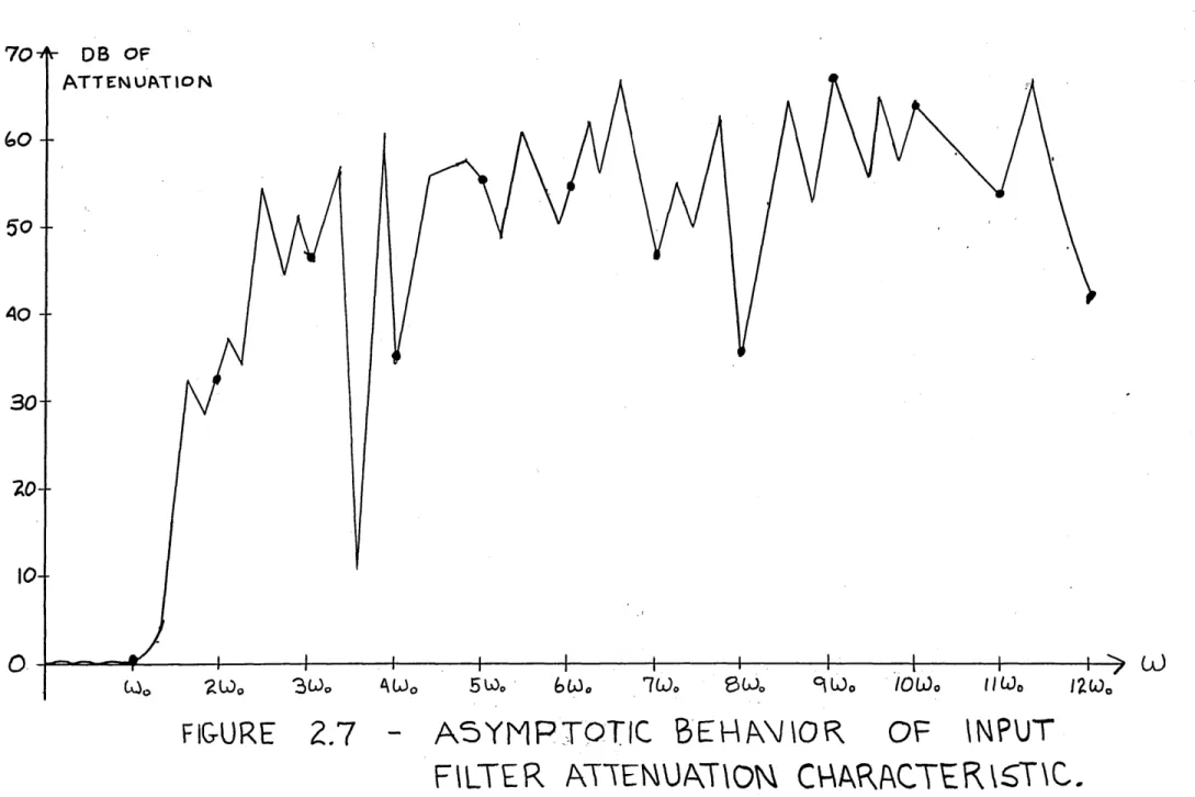
'70.Figure 2.7 presents an attenuation plot of the actual input filter. The spurious pass bands do not occur at the harmonics and the attenuation at the harmonics is always greater than ebout 30 db. The pass band losses are less than .5 db and the 3 db band edge is about 360. Mhz.
Table 2.1 is a summary of the predicted and actual attenua-tion characteristics of this low-pass filter. The predicted values are -remarkably accurate especially at the lower harmonics.
Table 2.1 -Frequency 0O 2 WO 3 ue 4 Wo 6 &. 7 W. 8 w.
9
w. 10 w. 12 W.e Comparison of Predicted Characteristics. Predicted Attenuation (from eq. 2.7)-(in db).44 32.5 45.3 36.7. 52.0 52.0 49.0 36.4 68.9 61.8 49.2 40.3
and Actual Low-Pass Filter
Actual Attenuation (from Fig. 2.7)-(in db)
.50 33.7 45.0 32.4 51.5 50.8 50.5 35.2 66.3 61.5 46.1 37.9
This chapter has described the input and output filters that are needed to realize the varactor frequency sextupler. The design considerations for each filter were given in detail. And one very important purpose of this chapter has been to demonstrate the use that a computer may be put to in the design and optimization of microwave filters.
CHAPTER III
DESIGN OF THE IMBEDDING NETWORK
Section 3.1 - Introduction
The design of a realizable imbedding structure for the diode that will expose the diode to the proper impedance levels
(as given in eqs. 0.2) is the essence of multiplier design. To be realizable, the imbedding network must be of a physical size that would permit its construction. Two solutions to this prob-lem are presented. The first is called the shorted stub approach and the second is the transformer approach.
The shorted stub structure (shown in Figure 3.1) is analogous to the lumped circuit realizations. In a lumped circuit multi-plier, the idler network ( imbedding network) consists of a re-sonant L-C circuit that shorts out the diode at each intermediate frequency between the input frequency and the desired output
frequency. Thus none of the intermediate harmonics appear in the output waveform. The shorted stub structure does essentially the same thing.
The transformer approach essentially uses a network such as the one in Figure 3.2 and, by choosing the proper lengths and impedances, comes up with a single structure that matches the required impedance function at all frequencies. The analysis of this network is done on a computer and the results are given in Section 3.3.
Section 3.2 - The Shorted Stub Method
In the shorted stub approach a number of stubs, equal to the harmonic number of the multiplier, extend outwardly from the diode. One stub is the input, one the output, and each of the others is
designed to "zero out" (match the impedance of the diode) at each intermediate frequency.
This is accomplished in the following manner. The impedance of a length '1' of transmission line, shorted at one end, is given,
TRNNSM!A5S\ON
UNE
STUBS
'TUN
NG
- P % '
3.1
rT w sHOR-sm57
N?? ROP\Ck-
"To
RAUDMG
THE
RQ.UR
15 A
STUb
FO?,, Th"E
N&Q,
NETNORK. T\-\E\
'D\O IDF -\OLVER
CONSTANT
DIAW\ETV
O\YVER CODUCOTOp\
VA\ASL
DmMETEP.
\NNER
CONUC7O?\
FI@UK
.
THE T~kRMW
kEAL1Z
NW
NETWJOR\K
THE REQ'JRD
IM~~
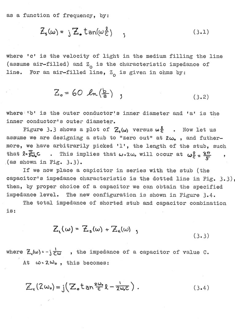
as a function of frequency, by:
where 'c' is the velocity of light in the medium filling the line (assume air-filled) and Zo is the characteristic impedance of line. For an air-filled line, Z is given in ohms by:
* (3.2)
where 'b' is the outer conductor's inner diameter and 'a' is the inner conductor's outer diameter.
Figure 3.3 shows a plot of Z,(w) versus w . Now let us assume we are designing a stub to "zero out" at 2w, , and futher-more, we have arbitrarily picked '1', the length of the stub, such that
=lC
. This implies that w=2-c0, will occur at .1.E(as shown in Fig. 3.3).
If we now place a capicitor in series with the stub (the
capacitor's impedance characteristic is the dotted line in Fig. 3.3), then, by proper choice of a capacitor we can obtain the specified impedance level. The new configuration is shown in Figure 3.4.
The total impedance of shorted stub and capacitor combination is:
Z
)
=L
+rZ(o)
(33)
where EJw- Cy, the impedance of a capacitor of value C.
At L2>ZLQ, , this becomes:
\J1
z
x,FIGURE
3.3
IMPEDANCE
VERSUS
FREQUENCY
FOR
STUB,
Zs (w)
)AND
TUNNG CAPAC\TORj
Zc(O).
1,
Zt=9.55
.okrnS.
SHORTED STU b CAPAC1TOR
TUNING
FIC-URE
PHY5\CAL
REALVZ
AT
\ON
OF
TAE
ClTAC\TOR
COME GURT\ON.
SCREW
Z4(w)
3.4
STU B
Z,
L)= Z,M
(LJ-
Z
co).
- TUN
\NC.
By substituting RZggC we have:
*
(3-5)
We set this impedance value equal to the value required in eqs. 0.3 for a specific diode and input frequency letting tan(I 3.08 we have, approximately:
.06.)
-
)
j
zx10
) =9.5~-~
(3.6)
for which we can pick values of Z and C.
For example, if Z = 68 ohms, then C would be about lOpf. And the stub length 'l' previously determined, would be about
30 inches. This length could be cut down considerably by making a better initial choice of the stub length.
But anyway, this example shows that it is certainly possible to realize the imbedding network by this method of shorted stubs. The capacitors that are required are available from Johanson Manufacturning Corporation, Boonton, New Jersey. They have
avail-able, cylindrical, variable capacitors of diameter.140 inches to about .300 inches in various ranges from .35pf to 30pf. They are rated throughout the UHF range and can be readily employed in this
design.
Tuning the capacitor to the desired impedance value may be done by using a hollow inner conductor for the stub and tuning through this opening.
So, by carrying out a similar procedure to the one above for the ?2,, stub, we can design each of the shorted stub resonators. Table 3.1 summarizes the imbedding network that was designed for the sextupler.
Stub "Zeros Out" Length of Stub Z of Stub Capacitance Needed
Number at- (in inches) (in ohms) (in pf)
S'3.95- 83.2 23.9 2 Z oC -
3.95~
83.2 2.4 3 3Woj-4=Z.%
48.5 2.0 4 A Wo .C Z 7.3'7 48.5 1.1 5 5' s Wc= ) 1.96 17.1 2.0 6 6v 1 6 17.1 1.5The capacitors that are required are all JMC - 4700
(.35 to 3.5pf) types except for the one in series with stub #1.
It is a JMC - 3908 (1 to 30pf) type. These capacitors will allow the imbedding network to be tuned for any value of C min between
8pf and 25pf. And typical values of C min for the diodes that were measured are between 16pf and 22pf. (See Table 1.7).
The only remaining problem with this design is to determine a way to bias the diode. If we imbed the top of the diode in a block of copper we can feed the bias in through a choke to the block. (See Figure 3.5). The block would also provide a good way to attach the stubs to the diode through the capacitor.
The above design then, shows a straight forward method to realize the imbedding network for the diode. It is a good way to approach the problem and will most likely be the easiest way to obtain a working sextupler.
~IAS TNC -R F C-R~OKE 5 401 TED ST AND C.RPACT SHORTEb A t CPP I10QDE
FIGURT
BIAS\
SCIE\AE
ST UB
FOR ID\ODF.
?\lRU-\2'T\ON
oF
~ET\P~O~KW
STUS F~AT~oR3.5
N
S ko?---7.ED
Section 3.3- Computer-Aided-Design of the Transformer Imbedding Structure
As a further example of computer-aided-design, another im-bedding network will be designed for the diode. This imim-bedding network will be in the configuration shown in Figure 3.2. The
four sections of transmission line will be chosen such that the impedance of the line will be nearly zero at all harmonics from the first through the sixth. The impedance of the parallel L-C combination, when added to the impedance of the transformer struc-ture, will match the diode impedance as specified in eqs. 0.2.
In a manner similar to the design of the low-pass input filter, a design for the transformer structure was chosen and optimized. Figure 3.6 is the computer analysis of the final structure. The
short at the end was assumed to have a small resistance (.01 ohms) to keep the functions from increasing without bound. The impedances
and lengths of line that were finally chosen are as follows: 11.86 inches of 40 ohm line, 5.56 inches of 45 ohm line, 4.61 inches of 50 ohm line and 1.63 inches of 55 ohm line. The optimization pro-cedure consisted of varying each of the four lengths (keeping the impedance constant) until the best combination was found.
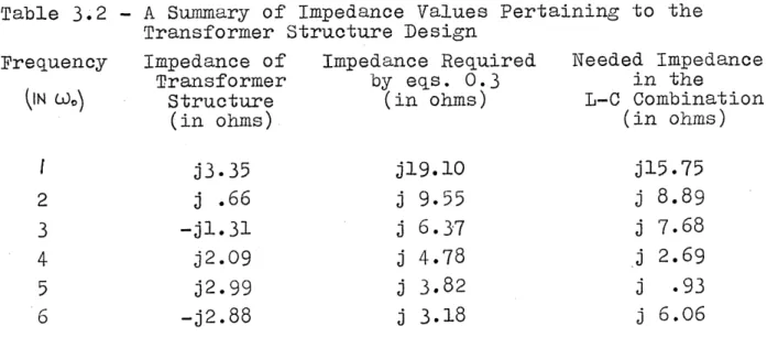
The difference between the impedance of the transformer struc-ture and that required in eqs. 0.3 must be made up by the L-C com-bination. Table 0.2 gives a summaryof these values.
Table 3.2 - A Summary of Impedance Values Pertaining to the
Transformer Structure Design
Frequency Impedance of Impedance Required Needed Impedance
Transformer by eqs. 0.3 in the
(IN
wo)
Structure (in ohms) L-C Combination(in ohms) (in ohms)
j3.35
jl9.10 jl5.75 2j
.66j
9.55 j 8.89 3 -jl.31 j 6.37j
7.68 4 j2.09j
4.78 j 2.69 5 j2.99j
3.82j
.93 6 -j2.88j
3.18 j 6.06ZLR(1)=.01,.01,.01,.01,.01,.01,.01, ZLI (1)=0. ,0. ,0. ,0. ,0. ,0. ,0. ZLI(1)=0.,0,0.0.0.0.,0.. LAM(1):7.,3.5,2.3333,1.75,1.4,1.1667,1.,N=7 LAM(1):7.,3.5,2.3333,1.75,1.4,1.1667,1.,N=7 Z(1)=40. ,45. ,50. ,55., Z(1):40. ,45. ,50. ,55., LC1)=1.75,.822,.6802,.24,NN=4* L(1)=1.75,.822,.6802,.24,NN=4* K L(K) 1 2 3 4 .175E .822E .680E .240E Z(K) 01 00 00 00 .400E .450E .500E .550E 02 02 02 02 K LA M (K) 1 .70000E 01 2 .35000E 01 3 .23333E 01 4 .17500E 01 5 .14000E 01 6 .11667E 01 7 .10000E 01
INPUT NUMBER OF VALUES N OF
LAM(1) AND NN OF Z(1),LAM(1),Z(1),L(1)
INPUT ZLR(1), Z LI(1) ZOR (K) .14250E-01 .12751E-01 .14693E-01 .1 1226E-01 .16991E-01 .14579E-01 .16025E-01
FIGURE
COMPUTER
\MBED\
N&
ANAL'\(S
1
NET WORK .
Z01(K) .33475E .66182E -. 13068E .20857E .29909E -.28826E -. 50571E 01 00 01 01 01 01 01OF TRAN5FORMER
F1G-URE
3, 7
WMPEDANCE
OF
AN
L-C PARALLEL
Figure 3.7 shows the impedance of a parallel L-C combination. By choosing the proper values for l and C we may place the positive
side of the impedance function at the correct points to realize the required impedance values as specified in Table 3.2. It would be wise to make the capacitance variable so the best match to the impedance function may be obtained. Here, the best match is defined as the point at which the output is maximized.
A good approximation to this parallel L-C combination would be an RF choke with a natural resonant frequency a little :more than 6x
(UO, (as shown in Fig. 3.7).
The bias for the diode may be fed in through the outer conduc-tor at any convenient point and the input and output may be taken by H-field loops at the low impedance end of the structure.
Actual values for L and C and details of construction have not been included in this paper because it is felt that this transformer network would be more difficult to realize than the shorted stub approach of the preceding section. The design procedures and con-sideration would have to be much more carefully worked out in order to make this an efficient multiplier.
The value of this approach lies in the fact that it proves that it is possible to realize the proper impedances with a single structure and that the computer may be used in the design and
CHAPTER IV
A SUMMARY OF IMPORTANT RESULTS AND CONCLUSIONS Section 4.1 - Summary
Many ideas have been presented in this paper so it would be worthwhile to collate these ideas and summarize the results that have been determined.
The major aim of this investigation was to demonstrate
that higher order frequency multipliers in the UHF and microwave ranges could indeed be realizably synthesized. The example of a sextupler was chosen and two possible realizations of this multi-plier were presented in Chapter III.
It should be emphasized that these results are not restricted merely to the sextupler but may however, be extended to other
higher order multipliers with little or no difficulty. The shorted stub approach may become a little unwieldy when applied to say, a X100 network. The design of such a structure, while not impossible, may warrant an attempt at having a stub "zero-out" on more than
one harmonic. With the proper choice of stub length and tunihg capacitor value, this is certainly possible.
Perhaps it would be better to approach the X100 problem with a single, transformer structure. It would be considerably more compact than the shorted stub approach but may require many more sections than the sextupler example used. Nevertheless, computer analysis of this network is indeed possible and this alone may preclude that intelligently designed high order frequency multi-pliers be of this type.
This leads to the other main conclusion that has been reached: that computer-aided-design is a valuable technique when applied to the design and optimization of microwave circuitry. CAD has proven its worth in many other areas of engineering and should be quite useful in microwave design especially since it is almost impossible in most cases to "breadboard" networks as can be done at the lower frequencies.
design of the transformer structure imbedding network and in the optimization of the imput filter design. Both of these examples have been thoroughly discussed already. It would be wise to mention, however, that the computer is not the ultimate answer to microwave design. The designer must be aware of the inherent limitations in constructing a specific microwave circuit.
For example, it would be very difficult to manufacture air-filled coax with a characteristic impedance greater than about 120 ohms without using a very large outer conductor or a very
small inner conductor. Also, it is unwise to specify dimensions with a tolerance tighter than about .0005 inch since this is the limit of most machine shop equipment. It is limitations like
these that must be imposed when using the computer for the analysis of microwave design problems.
Section 4.2 - Suggestions for Additional Investigations
The work undertaken for this thesis, while yielding a number of useful results, is by no means complete. Many doors to inter-esting and constructive reseach problems have been opened and it is the author's hope that ,at least some of these may be investi-gated.
The most exciting problem to be looked into yet is to verify that the multipliers that have been designed will actually work. Verification, of this result essentially involves constructing one or both of the imbedding networks and getting it to multiply.
Measurements could be made to determine how closely this network conforms to the impedance that the theory requires the diode see (eqs. 0.2). Determination of dynamic range, bandwidth and maximum output power would also prove valuable and instructive.
Another investigation could be made to try to find some sort of parallel circuitry that would permit the simultaneous use of
more than one diode. This would increase the maximum power handling capability of the multiplier.
The input filter was optimized on the computer and was assumed to be a continous series of unbent transmission line sections.
100 WATTS AT Wo 25 WATT5 oUT AT 33.