HAL Id: lirmm-01234455
https://hal-lirmm.ccsd.cnrs.fr/lirmm-01234455
Submitted on 26 Nov 2015
HAL is a multi-disciplinary open access
archive for the deposit and dissemination of
sci-entific research documents, whether they are
pub-lished or not. The documents may come from
teaching and research institutions in France or
abroad, or from public or private research centers.
L’archive ouverte pluridisciplinaire HAL, est
destinée au dépôt et à la diffusion de documents
scientifiques de niveau recherche, publiés ou non,
émanant des établissements d’enseignement et de
recherche français ou étrangers, des laboratoires
publics ou privés.
Use of CCD to Detect Terrestrial Cosmic Rays at
Ground Level: Altitude vs. Underground Experiments,
Modeling and Numerical Monte Carlo Simulation
Georgios Tsiligiannis, Luigi Dilillo, Alberto Bosio, Patrick Girard, Serge
Pravossoudovitch, Arnaud Virazel, Philippe Cocquerez, Jean-Luc Autran,
Antonio Litterio, Frédéric Wrobel, et al.
To cite this version:
Georgios Tsiligiannis, Luigi Dilillo, Alberto Bosio, Patrick Girard, Serge Pravossoudovitch, et al.. Use
of CCD to Detect Terrestrial Cosmic Rays at Ground Level: Altitude vs. Underground Experiments,
Modeling and Numerical Monte Carlo Simulation. IEEE Transactions on Nuclear Science, Institute
of Electrical and Electronics Engineers, 2014, 61 (6), pp.3380-3388. �10.1109/TNS.2014.2365038�.
�lirmm-01234455�
90 nm SRAM Static and Dynamic Mode Real-Time
Testing at Concordia Station in Antarctica
G. Tsiligiannis, L. Dilillo, A. Bosio, P. Girard, S. Pravossoudovitch, A. Virazel, P. Cocquerez, J. L. Autran,
A. Litterio, F. Wrobel, and F. Saigné
Abstract—In this work, we introduce the experimental setup and
the first results of the Real-Time testing platform of High Alti-tude Memory Test (HAMLET) project installed at the Concordia station in Antarctica (acceleration factor of 9.8 compared to New York City-NYC). The platform is dedicated for the study of the re-sponse of 90 nm Commercial Off The Shelf (COTS) Static Random Access Memories (SRAMs) to atmospheric neutrons, operating in both the static and dynamic modes. Based on the up-to-date ob-tained results, the Soft Error Rate (SER) of the devices is extracted and compared with accelerated SER data. The results reveal the appearance of phenomena such as Single Event Latchups (SELs) during SRAM operation under real conditions, and not only as a result of accelerated overstressing tests. Additionally, results are in agreement with the Joint Electron Device Engineering Council (JEDEC89) standard acceleration factor and the anisotropy of the neutron flux is also studied.
Index Terms—90 nm, atmospheric neutrons, Concordia station,
isotropy, real-time, SRAM.
I. INTRODUCTION
T
ERRESTRIAL radiation effects on electronic compo-nents have been studied extensively during the last two decades. The primary reason for this emerging concern lies onManuscript received July 11, 2014; revised September 13, 2014; accepted October 08, 2014. Date of publication October 30, 2014; date of current ver-sion December 11, 2014. This work was supported by the French “Agence Na-tionale pour la Recherche” (ANR) under the framework of the HAMLET project (ANR-09-BLAN-0155-01).
G. Tsiligiannis, L. Dilillo, A. Bosio, P. Girard, S. Pravossoudovitch, and A. Virazel are with the Laboratoire d’Informatique, de Robotique et de Microelec-tronique de Montpellier (LIRMM) Universite de Montpellier II/CNRS, 34095 Montpellier Cedex 5, France (e-mail: [email protected]; [email protected]; [email protected]; [email protected]; [email protected]; [email protected]; [email protected]).
P. Cocquerez, is with CNES, 31400, Toulouse, France (e-mail: [email protected]).
J. L. Autran is with the Aix-Marseille University, and also with CNRS, In-stitute of Materials, Microelectronics and Nanosciences of Provence (IM2NP,UMR CNRS 6242), MarseilleCedex 13, France (e-mail: [email protected]).
A. Litterio is with ENEA- Programma Nazionale di Ricerche in Antartide (PNRA) - Concordia Station - Dome C–Antarctica (e-mail: [email protected]).
F. Wrobel is with the Institut d’Electronique et Systèmes, Univers ite pellier II / CNRS, UMR-CNRS 5214, Place Eugene Bataillon - 34095 Mont-pellier Cedex 5, France, and also with Institut Universitaire de France, 75005 Paris, France (e-mail: [email protected]).
F. Saigné is with the Institut d’Electronique et Systèmes, Univers ite Montpel-lier II / CNRS, UMR-CNRS 5214, Place Eugene Bataillon - 34095 MontpelMontpel-lier Cedex 5, France (e-mail: [email protected]).
Color versions of one or more of the figures in this paper are available online at http://ieeexplore.ieee.org.
Digital Object Identifier 10.1109/TNS.2014.2363120
the reduction of the transistor size that makes electronic devices more sensitive to radiation. Since commercial applications have an increasing requirement for reliable electronic devices, re-search organizations and industry constantly explore mitigating mechanisms and try to understand the basic phenomena gener-ating failures as a result of natural radiation. To address these targets, radiation testing of electronic devices is one of the most fundamental procedures for reliability assessment.
Radiation testing of electronic devices can be classified in three different categories that work in a complementary way be-tween them: simulation based testing, accelerated testing under beam, and real-time testing (often referred as life testing). Sim-ulation based testing is among the fastest and cheapest methods, since it requires low resources besides the proper models of the studied devices [1], [2]. The drawback of this method is the lim-itation of the study of the radiation impact to a small number of transistors and not the entire device, because the computing time grows quickly with the complexity of the simulations. Testing in particle accelerator facilities is the most direct and fast method for the investigation of the response of an electronic device in actual radiating environment [3], [4]. The main drawback of this method is the cost, but also the fact that, in some cases, beam irradiation may induce artificial overstress of devices. The elevated flux of particles to which electronic devices are sub-jected may trigger phenomena that in actual real-time condi-tions will not occur. Accelerated results have been reported to differ to some degree from real-time results in [5], while in other cases more consistent results are obtained as in [6]. In [7], a comparison between different families of devices is performed showing that accelerated results may be in accordance or not with real-time testing results, depending also on the technology. Finally, real-time testing is considered to be the most reliable method of testing since it requires the components to be tested in their natural environment, while being exposed for a sufficient time to collect statistically significant data. Several studies, in the past and ongoing, are based on the exposure to natural ra-diation of large arrays of devices in several locations and for long periods (several months). In these devices the soft errors are collected and analyzed. The drawback of real-time testing is that it requires the integration of large scale platforms that can embed numerous components for accelerating the test duration, while at the same time they need to be exposed for a long pe-riod in order to collect sufficient data. In [8] a few hundreds of 40 nm SRAMS were tested at the high altitude desert Plateau de Bure (2552 m), in order to record their Soft Error Rate (SER) when exposed to atmospheric neutrons. For the same purpose,
0018-9499 © 2014 IEEE. Personal use is permitted, but republication/redistribution requires IEEE permission. See http://www.ieee.org/publications_standards/publications/rights/index.html for more information.
3390 IEEE TRANSACTIONS ON NUCLEAR SCIENCE, VOL. 61, NO. 6, DECEMBER 2014
two platforms using 90 nm and 130 nm SRAMs were placed at the Midi-Pyrénées Observatory (OMP, 2885 m) and the city of Puno in Peru (3889 m), as detailed in [9].
Continuing the effort of real-time testing of electronic de-vices, in this paper, we present the results achieved by the SRAM-based platform designed and developed at the Labo-ratoire d’Informatique, de Robotique et de Microélectronique de Montpellier (LIRMM) with the support of Institut d’Élec-tronique et Systèmes (IES) and the Centre National d’Études Spatiales (CNES) under the project High Altitude Memory Test (HAMLET). Under the same project other instruments have been installed at the same location such as silicon diodes and CCD sensors in order to cross validate the results occurring from the monitoring of the neutron flux, however, at the time of this publication the current experiments were the only ones able to provide with statistical data. The platform was placed at the Concordia scientific station in Antarctica [10], in 2013. In the present study, we introduce the design description of the platform, the retrieved results that allowed the estimation of the error rate of the sensing devices (SRAMs), but also the estima-tion of the atmospheric neutron flux and its characteristics (e.g. anisotropy) in this specific location. The results also prove that large-scale events (big clusters of bit-flips) may appear during real-time testing, and not only during accelerated testing. The interest behind this study is that Concordia station provides a unique environment in terms of altitude, longitude and latitude, and more specifically in terms of acceleration factor at ground level.
II. PLATFORM ANDENVIRONMENTSETUP
A. SRAM Based Neutron Detector Module
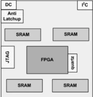
The test platform is composed of a large number of fun-damental modules, in which the sensing elements are 90 nm SRAMs. These modules are composed of four 32 Mbit COTS 90 nm Asynchronous SRAMs, which serve as Single Event col-lectors. The SRAMs are controlled by a Finite State Machine (FSM), which applies tests in both static and dynamic modes. The FSM is implemented into a FLASH-based FPGA, which is integrated into the same board, as depicted in Fig. 1. The choice of a FLASH based FPGA was made for its inherent robustness against radiation, so that to avoid SEUs occurring to other de-vices than the SRAM sensing components.
Within each testing module, the FSM applies tests in static mode in three of the four memories by writing a known se-quence (solid ‘1’s) and after a certain time threshold (set to twenty minutes), the entire content of the memories is read back. The choice of the solid ‘1’ data background was made because, from a previous study made on the same SRAM device [11], there is a higher sensitivity of the transition with respect to the transition ( ). During the read back, the con-tents of each word are compared with the expected sequence by the FSM and in the case of a detected upset, the erroneous word is written in a buffer, along with its address and the code of the memory. A master controller regularly downloads the experi-mental data from the buffer of each detecting module through a serial bus, which utilizes an communication protocol. Be-tween the read-back windows, the FSM applies a dynamic test
Fig. 1. SRAM based detection module composed of 4 32 Mbit COTS 90 nm Asynchronous bulk SRAM devices. The memories are controlled and tested by an FSM, which is implemented through a FLASH-based FPGA. Additional anti-latchup circuitry is added for the protection of the board. A JTAG interface allows the reprograming of the FPGA.
Fig. 2. Dynamic Stress March test. The test is composed of 6 elements (en-closed in parenthesis), and each element is composed of 7 operations. Each element (thus all the operations composing it) is applied to each word of the memory, and it advances in the memory address span in either an ascending or descending order indicated by the arrow in front of each element.
in the fourth SRAM of the detecting module. The applied test is the “Dynamic Stress” March test [11], in which a sequence of read/write operations is repetitively executed throughout the en-tire address span of the memory. March tests are algorithms that are utilized during the manufacturing process to reveal func-tional faults of memories such as coupling and stuck-at faults among others. The scheme describing the Dynamic Stress test is given in Fig. 2.
Each March test is composed of several elements, and each element is composed of several operations (in Fig. 2 the oper-ations of each element are enclosed in parenthesis). The March algorithms (Dynamic Stress in our case) are applied during irra-diation when the SRAM is exposed to a particle beam or during exposure in the natural environment, repetitively. The Dynamic Stress test is known to induce a Read Equivalent Stress (RES) to the memory cells, by applying multiple read operations in the same word. During a read access, the voltage levels of the node holding logic ‘1’ of the accessed cell are lowered as a result of the bit line discharge by opening the access transistor. The low-ering of the voltage of the node storing logic ‘1’ makes the cell more vulnerable to particle induced parasitic currents. At the same time, all the cells belonging to the same word line with the accessed ones will undergo the same stress (lowering of the logic ‘1’ voltage level) since their access transistors will be ac-tivated as well [12]. Besides the electric stress induced to the cells during the read operation, according to [13] where mem-ories of similar technology were studied, a low power scheme is applied to the SRAMs which keeps the entire memory in low voltage levels. During dynamic operations (read/write), instead
of powering the entire memory to nominal voltage, well-tap defined electric blocks are powered, inside which the word to be accessed belongs, for their execution. This scheme is ap-plied in order to avoid the occurrence of latchups (thanks to the low voltage preventing the triggering of Single Event Latchup (SEL)), and additionally limit them to the area defined by the electric blocks. By applying several read operations at the same word, the electric block the word belongs to will be powered for a prolonged period, enabling the potential occurrence of micro-latchups in that region.
During the Dynamic Stress test, the read operations are re-sponsible for the sensing of SEUs, and the upsets are imme-diately transmitted to the local buffer when detected. Within a module, the four memories share address and data buffers, and some of the control signal wires. Thus, the controller can ac-cess only one memory at the time. When the three memories that are tested in static mode are accessed for the read-back pro-cedure, the fourth memory that runs the dynamic test is set to standby mode. With the time window between two read-back operations significantly larger (20 minutes) than the duration of the read back time itself (for the 3 memories in static mode, it is less than 1 second), we can state that all four memories share the same experimental time.
Previous experiments made in particle accelerators using dy-namic mode testing on SRAMs have revealed higher cross sec-tion with respect to static mode testing and the appearance of several phenomena such as Single Event Functional Interrupts (SEFIs) or SELs [13] that were not observed with static mode. Thus, in addition to static test, the proposed test platform runs also dynamic tests with the joint purpose to maximize the ob-servation of events and try to confirm SEL and SEFI occurrence in the natural environment.
Besides the SRAMs and the FPGA, the detecting modules integrate additional circuitry such as a quartz oscillator for the generation of the clock used by the FPGA (running at 50 MHz), a voltage regulator and an anti-latchup component for the pro-tection of the overall module electronics. Finally, a JTAG inter-face allows the reprogramming of the FPGA device, in order to be able to apply modifications on the setup such as modifying the applied March test, modifying the exposure time window of the memories in static mode, or changing the data background of the memories in static mode.
B. Platform Setup
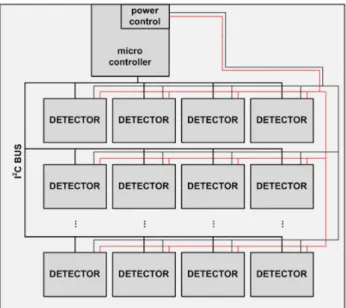
Each platform integrates 18 SRAM-based modules, making a total of 72 memories and 2304 Mbit capacity (approximately 2Gbit). A dedicated motherboard embeds the bus on which the 18 sensing modules are interconnected, as well as a micro-controller that plays the role of the master of the system. The interconnection bus is serial and uses the protocol. The bus was chosen for its free availability and for low power consumption purpose, since the communication protocol was not speed driven thanks to the low amount of data expected to circulate. The motherboard is also responsible for the power distribution to the detectors and the master microcontroller. The microcontroller is responsible for collecting and time-stamping the SEU information stored in the error buffers of each sensing module and transmitting them by email to our laboratory, in
France. For the communication between the microcontroller and the detecting modules, a Round-Robin protocol is imple-mented, during which the Master microcontroller sends in a cyclic manner a request for communication to each detecting module. Following, each detecting module responds to the master by transmitting the contents of its buffer in case it is not empty, or by just acknowledging it’s functioning. In the case after a request a timeout occurs (the detecting module does not respond to the communication query of the master) the master resets the nonresponding module. If the communication is restored, the Round-Robin continues its operation. In the case that communication is not restored, the device is deactivated by power switching-off and labeled as nonoperational. Between the executions of two Round-Robins, a certain time window elapses for the collection of the upsets. This time window is set to twenty minutes (same as the time window of the static test), in order to allow a significant amount of time to collect SEUs, but at the same time, to not overload the buffers in case of a major event such as micro-SEL or SEFI. Approximately, 2-3 emails are sent daily to our laboratory with the recorded upsets and the state of each detecting module (operational/not_operational). The model of the Round-Robin and the diagnostics procedures are part of the Finite State Machine implemented in the master and they have been modeled initially in UML language and tested under the SPIN verification tool [14], proving that no
livelocks or deadlocks are generated during execution. Further
details on the diagnostics procedures and the models that have been used can be found in the extended study presented in [15]. The final implementation of the master controller has been performed in C language as part of the microcontroller configuration. Due to connectivity problems, as a result of the Concordia station accessing internet through a satellite and being limited on power consumption, communications are not always guaranteed. However, the data, which are meant to be transferred, are not lost in case of email sending failure, and the microcontroller assures their proper transmission. Fig. 3 illustrates a functional scheme of the test platform.
In the Concordia station, we installed two identical test plat-forms, for a total amount of 4608 Mbit. In order to explore anisotropy of atmospheric neutrons in Concordia, one platform has been mounted horizontally (Machine X), while the other one vertically (Machine Y).
C. Concordia Station
The Concordia station is located at an altitude of 3233 m in Antarctica ( ) in the department called Dome C of the Antarctic Plateau [10]. It is one of the coldest places on Earth, with temperatures ranging from down to . Due to its location, a very high flux of atmospheric neutrons is expected (according to JEDEC standard, an acceleration factor of 9.81 is expected with respect to the NYC measurements [16]). The room in which the instruments operated was under constant temperature of .
III. RESULTS ANDANALYSIS
During the analysis of the retrieved results, certain guide-lines have been followed in order to make the results more re-liable and avoid misinterpretations. One of the most important
3392 IEEE TRANSACTIONS ON NUCLEAR SCIENCE, VOL. 61, NO. 6, DECEMBER 2014
Fig. 3. SRAM based detector platform. In this platform, 18 detecting modules are mounted, and each one of them integrates four 32 Mbit 90 nm SRAMs. A microcontroller is responsible for the data collection of each detector via an bus. A motherboard interconnects all the detectors with the microcontroller and distributes the power.
aspects of the study is the proper calculation of the occurring upsets, since they represent the major metric. For this reason, a neighboring scheme was adopted to classify Multiple Cell Upsets (MCUs), SEFIs and other types of large-scale events such as Single Event Latchup. In Table I, we provide both the event counts and the total number of corrupted bits as they were recorded. This scheme follows a –bit neighboring policy, in which corrupted bit-cells that have a physical distance smaller or equal than three bits are considered the result of the same event. The timestamp has been taken into account as well for the clustering procedure, but it is rather unlikely to observe two events occurring in such a small topological distance (equal to three bits), since the event rate is approximately 1-2 events per day for 2304 Mbit. The software that was used for this purpose has been extensively successfully utilized and validated with data coming from accelerated tests. The data in Table I have been processed to obtain the graphs in Fig. 4 and Fig. 5.
Through the count of the failing bits and the study of their position in the physical bitmap of the memory, we were able to identify Single Bit Upsets (SBUs), MCUs, and other major events such as micro-SELs. Table I provides the information concerning the SER as calculated, considering the events count and the total count of corrupted bits (
respectively), while in parenthesis information regarding the standard error of the Poisson distribution is provided.
In order to better understand the obtained results, it is essen-tial to normalize the SER with a known reference position, such as the NYC. Considering the acceleration factor of 9.81 given by JEDEC standard, the SER of 14858FIT/Mbit ( ) at Con-cordia for Machine Y will correspond to an SER of 1514FIT/ Mbit at NYC and the SER of 13754FIT/Mbit ( ) of Ma-chine X corresponds to an SER of 1402FIT/Mbit at NYC. By comparing these results to recent results obtained with acceler-ated tests, we can have a more global figure of the SER response
Fig. 4. Bit failure count plot for the two test platforms. Considering the av-erage number of received failures w.r.t. the number of days the machines were operational, a failure rate of 1.05 bits/day is calculated for the 2304 Mbits.
Fig. 5. Cumulative plots of the bit failures (total number of corrupted bits) and of the events (SBUs are counted as one event and MCUs as well) for both ma-chines. Considering the results of Fig. 3, the steep parts of the plots are explained from the occurrence of major events.
TABLE I
EXPERIMENTALDATASUMMARY
of the memories under study. Based on accelerated under beam experiments for the same memories, the cross section was found to be cm bit when irradiated at the ISIS facili-ties with neutrons that approach the atmospheric spectra of en-ergies from 10-800 MeV [17]. This cross section corresponds
to an SER of 1742FIT/Mbit at NYC with a standard error of 16%. These results reveal that the difference between acceler-ated tests and life testing can be small (less than 20% which is part of the expected statistical error). Nevertheless, past studies have shown different results as in [5] or [6] where accelerated tests have given slightly higher estimation of the device error rate. As mentioned in [6] several reasons can explain a rele-vant deviation between accelerated testing and real-time testing such as errors induced by the flux calculation in the accelerator facilities, errors induced by the acceleration factor calculation, variability, aging etc.
Observing the results from Table I, we can observe the differ-ence between the occurring upsets when the memories operate in Static mode and in Dynamic mode. The results show that Static mode testing provides more events with respect to Dy-namic mode testing, and specifically the DyDy-namic Stress March algorithm that was chosen. This result goes against previous experimental data from accelerated testing, during which the Dynamic Stress March algorithm proved to provide the highest cross section among different dynamic tests and the static test. The difference in the number of occurring events is 30–50% lower for the Dynamic Stress test with respect to the static. The difference on the occurring events in both platforms between static and dynamic mode, can be attributed to two main reasons. The first reason is the lack of sufficient statistical data that can justify these results. When comparing the data occurring from dynamic and static mode testing, the lack of sufficient data oc-curring during dynamic mode testing, does not allow the gener-ation of a solid result. Future measurements will reveal a more solid outcome. The second reason is that during dynamic mode testing, two effects work in opposite directions with respect to the SRAM cell robustness. Although the Dynamic Stress algo-rithm induces the RES to the cells of the array making them weaker, at the same time, a portion of the SRAM cell array de-fined by the electric blocks is powered at nominal . The powering of the cells at nominal makes them more robust with respect to cells that remain in low power mode. Consid-ering the results collected so far, the low power mode during static mode testing seems to dominate the sensitivity with re-spect to the RES induced during Dynamic Stress test. Additional data collected from the Concordia station will shed more light on this part of the study. The overall SER of both Machine X and Y was calculated by considering both the tests in static and dynamic mode. This scheme was considered for the reason of data accumulation in the short period of exposure so far, but also of a more realistic behavior of a system where SRAM devices operate in both the static and dynamic mode.
A. Neutron Isotropy
Comparing the results from the two instruments, we can also observe that instrument X (horizontally placed), has a smaller failure rate ( %) with respect to instrument Y (vertically placed). Such a small variance can be related either to a statis-tical error or to an actual minor effect of flux anisotropy. Further collection of data is necessary to strengthen the validity of the low effect of anisotropy.
B. Deceptive Failures Due to Permanent Defects
As already described above, interesting effects were observed during testing. Instrument Y presented some repetitive failures that affected a certain number of cells and that did not occur systematically or periodically. For example, some bits in a few consecutive words have been failing only few times during the 8-month period of the experiment. These events were not sys-tematic, but they appeared as deceptive faults. This probably means that permanent reduction of the reliability of a group of cells has occurred, but this implies the normal function of these cells for most of the time for both retention and access. On the other hand, some concurrent stress conditions such as the dy-namic access, noise on the power line and/or particle hit (that singularly would not be able to trigger events) may stimulate this weakness and cause errors. The lowering of reliability may be the result of device aging, electromagnetic interferences, de-fective devices (considering the total amount of devices used for these platforms), or radiation-induced defects. Currently, the platforms have not been retrieved yet, and thus we cannot pro-vide any additional information.
C. Large-Scale Errors
Another interesting observation that was made as part of the real-time testing that we performed at Concordia was the occur-rence of a few micro-SELs. As can be seen from Fig. 4, there are some points that indicate a large increment of the failing bits, in a single day. This increment is not the result of multiple MCUs, but rather the occurrence of an SEL that was limited in a small region of the memory. Fig. 6 gives an example of such an event, where each pixel in black corresponds to a corrupted bit, and each pixel in white corresponds to a noncorrupted bit. In [13], similar micro-SELs have been observed in the same SRAMs while irradiating them with a neutron beam with a spectrum that approaches the atmospheric one. These latchups do not propa-gate to the entire memory, but they affect a significant number of cells (few hundreds) belonging to a rectangular region de-fined by the presence of well-taps [13]. As previously explained, thanks to the adopted low-power scheme, the largest part of the memory array is kept in retention mode with low voltage, and only the selected electric block (where the read/write access is made) is powered with nominal voltage. The electric block is defined with respect to the n- and p-well tap positioning. Ac-cording to [18] only the nominal voltage allows the triggering of latchup that cannot spread to the rest of the memory array because of the well-tap barrier and the low voltage in the unse-lected blocks. The observation of such events during real-time testing is of critical importance, since it demonstrates that they may occur not only under accelerated conditions, but also in real-time. Moreover, such events do not require the power reset of the device, since at the end of the operation cycle the affected block is fed with low voltage and the latchup is removed. On the memory bitmap, these SELs appear as large scale MCUs, as shown in Fig. 5.
D. Environmental Phenomena
For the platforms operating in Antarctica, there has been the opportunity to observe additional phenomena that in normal conditions, they would not face. The most important one has
3394 IEEE TRANSACTIONS ON NUCLEAR SCIENCE, VOL. 61, NO. 6, DECEMBER 2014
Fig. 6. Physical bitmap representation of the memory under test. In this figure, a SEL is propagated to a well-tap defined region of the memory. Pixels in white denote noncorrupted bit-cells, while pixels in black correspond to corrupted cells.
been the aurora australis (southern light), which occurs sev-eral times every year. Aurora Australis is the light emitted when charged particles (electrons and protons) enter the Earth’s at-mosphere and collide with other atoms. During the experiments, several aurora australis occurred at Concordia, and, in partic-ular, one episode lasted for many hours between the days 14th and 15th of July 2013. During these events the SEU sensing platforms were operational (no communication or power supply problems), but the recorded data do not show any difference in the error rate w.r.t. normal conditions. Such an observation shows that these particles did not reach the devices, since their charge has been absorbed by the atmosphere in higher altitudes and/or the structure of the building and the device packaging.
A phenomenon that could potentially induce a significant dif-ference on the performed measurements, are the Ground Level Enhancements (GLEs)[19]. These events are the result of Solar Energetic Particle (SEP) events, during which particles of en-ergies up to the GeV level reach the ground level as a result of the SEPs collision to the earth’s atmosphere. Such particles can potentially induce SEUs to the memory devices, thus increase the observed rate of errors. However, during the period of ex-posure the data have been collected (April-November 2013), no Ground Level Enhancement (GLE) events have been reported. The two latest GLE events have occurred in May 2012 and Jan-uary 2014 according to [20].
IV. CONCLUSION
In this paper, we introduced the experiment made through an SEU detecting platform for real time testing that operated at the Concordia Station in Antarctica. The retrieved results validated the acceleration factor of the referenced atmospheric neutron flux in the Concordia station, as well as the error rate of the SRAMs under study for such environments. Considering the flux acceleration factor that was found with respect to the one of NYC, similar experiments placed in Pic Du Midi for example, would require either more exposure time ( ) so that enough statistical data are gathered, or larger memory arrays. Interesting phenomena have been recorded such as the occur-rence of micro-SELs, proving that these events are not occurring only in accelerated testing environments, but they appear also in real-life applications. The different orientation of the sensing devices (SRAMs) during experiments has demonstrated a good isotropic distribution of the neutron flux. Finally, it was shown that Southern Lights do not have an actual impact on the number of recorded events.
ACKNOWLEDGMENT
The authors would like to acknowledge the Institut Polaire Français Paul Emile Victor (IPEV) and the Italian Programma
Nazionale Ricerche in Antartide (PNRA) for providing access and logistics support at the Concordia station.
REFERENCES
[1] R. Naseer, Y. Boulghassoul, J. Draper, S. Dasgupta, and A. Witulski, “Critical Charge Characterization for Soft Error Rate Modeling in 90 nm SRAM,” in Proc. IEEE ISCAS, May 26–30, 2007, pp. 1879–1882.
[2] T. Heijmen, D. Giot, and P. Roche, “Factors that impact the critical charge of memory elements,” in Proc. IEEE IOLTS, 2006, pp. 57–62. [3] P. Roche, G. Gasiot, K. Forbes, V. O’Sullivan, and V. Ferlet, “Compar-isons of soft error rate for SRAMs in commercial SOI and bulk below the 130-nm technology node,” IEEE Trans. Nucl. Sci., vol. 50, no. 6, pp. 2046–2054, Dec. 2003.
[4] G. Tsiligiannis, L. Dilillo, A. Bosio, P. Girard, A. Todri, A. Virazel, A. D. Touboul, F. Wrobel, and F. Saigne, “Evaluation of test algorithms stress effect on SRAMs under neutron radiation,” in Proc. 2012 IEEE
18th IOLTS, 2012, pp. 121–122.
[5] H. Puchner, “Correlation of life testing to accelerated soft error testing,” in Proc. 3rd Annu. IEEE SER Workshop, CA, USA, 2011, pp. 1–23.
[6] J. L. Autran, P. Roche, S. Sauze, G. Gasiot, D. Munteanu, P. Loaiza, M. Zampaolo, and J. Borel, “Altitude and Underground Real-Time SER Characterization of CMOS 65 nm SRAM,” IEEE Trans. Nucl. Sci, vol. 56, no. 4, pp. 2258–2266, Aug. 2009.
[7] A. Lesea, S. Drimer, J. J. Fabula, C. Carmichael, and P. Alfke, “The rosetta experiment: Atmospheric soft error rate testing in differing tech-nology FPGAs,” IEEE Trans. Device Mater. Rel., vol. 5, no. 3, pp. 317–328, Sep. 2005.
[8] J. L. Autran, S. Serre, D. Munteanu, S. Martinie, S. Semikh, S. Sauze, S. Uznanski, G. Gasiot, and P. Roche, “Real-time Soft-Error testing of 40 nm SRAMs,” in Proc. IEEE IRPS, Apr. 15–19, 2012, pp. 3C.5.1–3C.5.9.
[9] G. Hubert et al., “Continuous high-altitude measurements of cosmic ray neutrons and SEU/MCU at various locations: Correlation and analyses based-on MUSCA SEP 3,” IEEE Trans. Nucl. Sci., vol. 60, no. 4, pp. 2418–2426, Aug. 2013.
[10] [Online]. Available: Concordia Station webpage: http://www.institut-polaire.fr/ipev/bases_et_navires/station_concordia_dome_c
[11] P. Rech, J.-M. Galliere, P. Girard, A. Griffoni, J. Boch, F. Wrobel, F. Saigne, and L. Dilillo, “Neutron-Induced Multiple Bit Upsets on Two Commercial SRAMs Under Dynamic-Stress,” IEEE Trans. Nucl. Sci., vol. 59, no. 4, pp. 893–899, Aug. 2012.
[12] A. Bosio, L. Dilillo, P. Girard, S. Pravossoudovitch, and A. Virazel,
Advanced Test Methods for SRAMs - Effective Solutions for Dynamic Fault Detection in Nanoscaled Technologies. New York, USA:
Springer, 2010.
[13] G. Tsiligiannis, L. Dilillo, A. Bosio, P. Girard, S. Pravossoudovitch, A. Todri-Sanial, A. Virazel, H. Puchner, C. Frost, F. Wrobel, and F. Saigné, “Multiple-Cell-Upsets Classification in commercial SRAMs,”
IEEE Trans. Nucl. Sci., vol. 61, no. 4, pp. 1747–1754, Aug. 2014.
[14] SPIN Model checker [Online]. Available: http://spinroot.com/spin/ whatispin.html
[15] L. Dilillo, A. Bosio, M. Valka, P. Girard, S. Pravossoudovitch, and A. Virazel, “Error resilient infrastructure for data transfer in a dis-tributed neutron detector,” in Proc. 2011 IEEE Int. Symp. DFT, 2011, pp. 294–301.
[16] Measurement and Reporting of Alpha Particle and Terrestrial Cosmic Ray-Induced Soft Errors in Semiconductor Devices, JEDEC Test Stan-dard, no. 89A, 2006.
[17] ISIS Rutherford Appleton Laboratory [Online]. Available: http://www. isis.stfc.ac.uk/
[18] D. J. Sleeter and E. W. Enlow, “The relationship of holding points and a general solution for CMOS latchup,” IEEE Trans. Electron Devices, vol. 39, no. 11, pp. 2592–2599, Nov. 1992.
[19] I. G. Usoskin, G. A. Kovaltsov, I. A. Mironova, A. J. Tylka, and W. F. Dietrich, “Ionization effect of solar particle GLE events in low and\middle atmosphere,” Atmos. Chem. Phys., vol. 11, no. 5, pp. 1979–1988, Mar. 2011.
[20] N. Thakur, N. Gopalswamy, H. Xie, P. Makela, S. Yashiro, S. Akiyama, and J. M. Davila, “Ground Level Enhancement in the 2014January 6 Solar Energetic Particle Event,” arXiv:1406.7172 [astro-ph], Jun. 2014.