HAL Id: tel-01222167
https://tel.archives-ouvertes.fr/tel-01222167
Submitted on 29 Oct 2015HAL is a multi-disciplinary open access
archive for the deposit and dissemination of sci-entific research documents, whether they are pub-lished or not. The documents may come from teaching and research institutions in France or abroad, or from public or private research centers.
L’archive ouverte pluridisciplinaire HAL, est destinée au dépôt et à la diffusion de documents scientifiques de niveau recherche, publiés ou non, émanant des établissements d’enseignement et de recherche français ou étrangers, des laboratoires publics ou privés.
spintronic applications
Tiantian Zhang
To cite this version:
Tiantian Zhang. Spin injection in III-V semiconductor-based systems for spintronic applications. Mi-cro and nanotechnologies/MiMi-croelectronics. INSA de Toulouse, 2014. English. �NNT : 2014ISAT0005�. �tel-01222167�
TH `
ESE
TH `
ESE
En vue de l’obtention du
DOCTORAT DE L’UNIVERSIT´
E DE TOULOUSE
D´elivr´e par : l’Institut National des Sciences Appliqu´ees de Toulouse (INSA de Toulouse)
Pr´esent´ee et soutenue le 09 avril 2014 par :
Tiantian ZHANG
Injection de spin dans des syst`
emes
`
a base de semiconducteurs III-V
en vue de nouveaux composants spintroniques
JURY
Rapporteur Paul VOISIN Directeur de Recherche, LPN-CNRS, Marcoussis Rapporteur Matthieu JAMET Directeur de Recherche, CEA, Grenoble
Examinateur Jacques PERETTI Directeur de Recherche, LPMC-Polytechnique, Paris Examinateur Lionel CALMELS Professeur, Universit´e Paul Sabatier, Toulouse Directeur de th`ese Pierre RENUCCI Professeur, LPCNO-INSA, Toulouse
CoDirecteur de th`ese H´el`ene CARRERE Maˆıtre de Conf´erence, LPCNO-INSA, Toulouse
´
Ecole doctorale et sp´ecialit´e :
Science de la mati`ere: Nanophysique Unit´e de Recherche :
Laboratoire de Physique et Chimie de Nano-Objets, INSA-CNRS-UPS (UMR 5215) Directeur(s) de Th`ese :
Pierre RENUCCI et H´el`ene CARRERE Rapporteurs :
R´
esum´
e de Th`
ese
Sp´ecialit´e: Nanophysique Nom: ZHANG
Pr´enom: Tiantian
Titre de la th`ese en fran¸cais: Injection de spin dans des syst`emes `a base de semiconducteurs III-V en vue de nouveaux composants spintroniques
R´esum´e de la th`ese en fran¸cais:
La spintronique dans les semiconducteurs vise `a utiliser le spin de l’´electron comme degr´e de libert´e suppl´ementaire (en plus de la charge ´electrique) afin de v´ehiculer l’information, ce qui permettrait la mise au point de composants int´egrant de nouvelles fonctionnalit´es. Ce travail de th`ese porte sur deux ´etapes importantes qui doivent ˆetre maˆıtris´ees : l’injection ´electrique de porteurs polaris´es en spin dans les semiconducteurs III-V, et la manipulation du spin de l’´electron (par champ magn´etique) dans ces mat´eriaux optimis´es. Dans un premier temps, la grande efficacit´e des in-jecteurs de spin `a base de CoFeB/MgO/GaAs est d´emontr´ee dans des dispositifs de type Diodes Electroluminescentes polaris´ees en spin (SpinLEDs). La comparaison entre des injecteurs comprenant une barri`ere tunnel fabriqu´ee soit par pulv´erisation cathodique, soit par ´epitaxie par jets mol´eculaires (MBE), permet de montrer que ces deux techniques don-nent des r´esultats comparables. Dans les deux cas, l’efficacit´e de l’injection est am´elior´ee par un recuit de l’´echantillon autour de 300−350◦C. Le recuit induit une am´elioration de la qualit´e de l’interface CoFeB/MgO. De plus, l’efficacit´e de l’injection de spin n’est stable en fonction du courant inject´e que lorsque la barri`ere tunnel est fabriqu´ee par pulv´erisation cathodique. Ceci est dˆu aux caract´eristiques de l’interface MgO/GaAs qui diff`erent selon la technique de croissance de la barri`ere. Dans un deuxi`eme temps, l’injection de spin en l’absence de champ magn´etique externe appliqu´e est r´ealis´ee grˆace `a un nouveau type d’injecteur constitu´e d’une ´electrode de CoFeB ultrafine pr´esentant une aimantation r´emanente de la couche le long de l’axe de croissance de l’´echantillon. Pour la premi`ere fois des taux de polarisation circulaire de l’´electroluminescence de l’ordre de 20% sont mesur´es `a 25 K `a champ magn´etique nul. Ensuite, la probl´ematique de la relaxation de spin des porteurs inject´es dans les vall´ees L de haute ´energie dans GaAs (ph´enom`ene non n´egligeable sous injection ´electrique) est ´egalement trait´ee. Nous observons qu’une fraction de la m´emoire du spin photog´en´er´e en L est conserv´ee lorsque les ´electrons sont diffus´es vers la vall´ee Γ, malgr´e une relaxation d’´energie de plusieurs centaines de meV. Le temps de relaxation de spin dans les vall´ees L est estim´e autour de 200 fs. Enfin, nous avons explor´e le mat´eriau GaAsBi dilu´e (x∼ 2.2%) dont la perturbation de la matrice par l’´el´ement Bi permet d’attendre des propri´et´es ´electroniques et de spin fortement modifi´ees. Des mesures de photoluminescence ont mis en ´evidence une diminution de l’´energie de bande interdite de l’ordre de 85meV/%Bi. De plus, par la mesure directe des battements quantiques de la polarisation de photoluminescence nous avons d´etermin´e un facteur de Land´e des ´electrons de conduction de l’ordre de deux fois sup´erieur `a celui de GaAs. Ces r´esultats t´emoignent de la forte perturbation des ´etats de valences et de l’augmentation de l’interaction spin-orbite.
Titre de la th`ese en anglais: Spin injection in III-V semiconductor-based systems for spintronic applications R´esum´e de la th`ese en anglais:
Spintronics of semiconductors aims at using carrier spins as supplementary means of information transport. This would lead to components showing extended functionalities. This thesis work is dedicated to the study of injection and manipulation of electron spin in semiconductors, which are the basis of any spintronic application. In a first step we demonstrate the high efficiency of CoFeB/MgO/GaAs - based spin injectors. Circular polarization degrees of elec-troluminescence over 20% are measured on spin polarized LEDs (SpinLEDs) at 0.8 T and 25 K. Comparison between sputtering- and MBE- grown spin injectors has shown similar results. In both case, spin injection efficiency is increased by thermal annealing of the sample, in the range 300− 350◦C. Indeed, annealing improves the quality of CoFeB/MgO
interface, and induces the crystallization of CoFeB above 300◦C. A higher stability of spin injection with current
in-jection is found when the tunnel barrier is grown by sputtering. This is due to the MgO/GaAs interface characteristics which is related to the growth technique. In a second step, we demonstrate spin injection without external applied magnetic field, through an ultra-thin (a few atomic layers) CoFeB electrode, taking advantage of the perpendicular magnetic anisotropy of the layer which leads to a remanant magnetization along the growth axis. For the first time in this configuration, circular polarization degrees of electroluminescence of about 20% are measured at 25 K at zero magnetic field. In a third step, due to the crucial role it may play in electrical injection, electron spin dynamics in high energy L-valleys is investigated. Using polarization resolved excitation photoluminescence in the range 2.8-3.4 eV, we observe that a fraction of photogenerated spin polarization is preserved when electrons are scattered hundreds of meV down to Γ valley. Spin relaxation time in L valleys is estimated to 200 fs. Finally we investigate electron and spin properties of GaAsBi dilute bismide alloy. We observe that the bandgap energy is reduced by 85meV/%Bi when Bi element is introduced into GaAs matrix. Moreover, the electron Land´e factor is about twice the one in GaAs for a 2.2% Bi composition. These features are evidence of the strong perturbation of host states and spin-orbit interaction enhancement.
Remerciements
Avant d’exposer mon travail de th`ese, je voudrais remercier toutes les personnes qui m’ont apport´e, de pr`es ou de loin, leur encouragement, leur soutient, leur aide, leur
amiti´e . . .
En premier lieu, je remercie P. Voisin et M. Jamet pour avoir accept´e d’ˆetre rap-porteurs de cette th`ese. Je remercie ´egalement J. Peretti et L. Calmels pour leur
participation `a ce Jury en tant qu’examinateurs.
Merci `a toute l’´equipe d’opto´electronique quantique du LPCNO (Laboratoire de
Physique et Chimie des Nano-Objets) pour m’avoir accueillie et guid´ee tout au long de ces trois ann´ees et demi :
Je voudrais tout d’abord dire un grand merci `a mon superviseur Prof. Pierre Renucci, qui a ´et´e ,tout au long de cette th`ese, tr`es gentil et serviable. Merci de m’avoir aider
lors de mon arriv´e `a Toulouse, de m’avoir pr´esent´e `a toute l’´equipe du LPCNO, de m’expliquer toutes les choses dans le laboratoire, de nous voir presque tous les soirs
dans la salle de manip et de nous discuter avec nous des nouveaux r´esultats...
Je voudrais ensuite remercier `a la co-directeur de th`ese H´el`ene Carr`ere de m’avoir
aid´ee rapidement a chaque fois que j’avais un probl`eme, et d’avoir ´et´e aussi joilleuse et enthousiaste. Ce fut tr`es agr´eable de travailler avec toi dans le mˆeme bureau durant
ces 3 ans.
Un grand Merci `a Thierry Amande et Xavier Marie, d’avoir pris le temps de
m’expliquer les m´ecanismes de spintronique et pour lesquels j’ai pu b´en´eficier de con-seils constructifs et d’explications lumineuses.
Merci `a Andrea Balocchi et D´elphine Lagarde de m’avoir aid´e `a r´egler des probl`emes de r´eglage du laser lorsque je commencais `a peine `a travailler avec celui-ci.
Merci `a Philippe Barate, Simone Mazzucato, Cong Tu Nguyen, Meal Vidal, pour toute l’aide que vous m’avez apport´e lors des manipulations. Merci pour la bonne
ambiance que vous avez su mettre dans la salle de manip. Merci aussi `a Bernhard Urbaszek, Louis Bouet et Gang Wang.
Je remercie les secr´etaires de notre laboratoire et Madame Fortun´e, qui m’ont beau-coup aid´e pour les dossiers administratifs.
Merci `a Y. Lu, S. H. Liang, X. Devaux, C. Fontaine and A. Arnoult, J.-M. George, H. Jaffr`es, J. Frougier, B. Xu, X. D. Qin d’avoir pr´epar´e les ´echantillons ainsi que pour
Juan, Hong, Lijian, Tao, Xiaojian, Wuwei, Hang, Wenjun, Chengcheng, Xu, Dong-dong, Haojun, Xiaoxiao, Yanping, Rui, Yu, mes colocataires David et Juana... pour
les conseils de vie dans un pays qui ´etait pour moi totalement nouveaux, pour les voy-ages qui m’ont permise de visiter de nouveau pays et pour toutes ses soir´ees que l’on a
pass´e ensemble. Merci `a tous mes amis en chine: Yufei, Yuan, Yuzhou, Bingnan, Peng, Jinghua, Yue, Fang, Linlin, Yang... pour les encouragements et l’aide que vous m’avez
apport´e.
Je remercie les organisateurs du programme CSC/UT-INSA dont le financement a
facilit´e ma venue en France pour r´ealiser ma th`ese.
Un tr`es grand Merci `a mes parents pour m’avoir encourag´e `a partir faire mes ´etudes
en France, merci `a eux de toujours ˆetre pr´esent pour moi.
Et enfin Merci pour cette rencontre inattendu, rencontre qui m’a permise de voir
et faire des choses que je ne pouvais voir que dans les films. Merci `a toi Emmanuel l’amour de ma vie.
Un grand MERCI `a vous tous!
Contents
Abstract i
Remerciements iii
Introduction 1
1 Introduction to the properties of zinc blende III-V semiconductors 7
1.1 III-V semiconductors band structure . . . 9
1.1.1 Bulk semiconductors . . . 9
1.1.2 Semiconductor heterostructures . . . 12
1.2 Optical orientation in zinc-blende semiconductors . . . 17
1.2.1 Optical transitions . . . 17
1.2.2 Optical selection rules . . . 18
1.3 Main spin relaxation mechanisms . . . 21
1.3.1 D’Yakonov-Perel Mechanism . . . 21
1.3.2 Elliott-Yafet Mechanism . . . 22
1.3.3 Bir-Aronov-Pikus Mechanism . . . 23
1.3.4 Electron spin relaxation due to the Hyperfine-interaction . . . . 23
1.4 Electrical spin injection into Spin-LEDs . . . 24
1.4.1 Problem of impedance mismatch in the diffusive regime . . . 25
1.4.2 Spin Light Emitting diodes as a tool to detect and quantify elec-trical spin injection . . . 30
1.4.3 State of the art: breakthrough due to MgO tunnel barriers . . . 33
2 Experimental Set-ups 39 2.1 Time-resolved Photoluminescence spectroscopy . . . 41
2.1.1 Excitation laser source . . . 41
2.1.2 Streak camera detection . . . 42
2.1.3 Polarization resolution . . . 45
2.2 Polarization-resolved Electroluminescence set-up . . . 45
2.2.1 CCD camera detection . . . 46
2.2.2 Electrical generator . . . 47
2.3 Polarized Photoluminescence Excitation spectroscopy . . . 47
2.4 Cryogenics and magnetic field . . . 49
3 Electrical spin injection in Spin-LEDs 51 3.1 Influence of the growth technique (Sputtering and Molecular Beam Epi-taxy) . . . 55
3.1.1 Spin-LEDs Samples . . . 56
3.1.2 Electroluminescence measurements . . . 57
3.1.3 Influence of the annealing process on the spin injection efficiency 58
3.1.4 Measurement of the electron lifetime and spin relaxation times in the InGaAs/GaAs quantum well by Time and
Polarization-resolved Photoluminescence . . . 59
3.1.5 Analysis of the influence of the annealing process on the hystere-sis curves of the ferromagnetic layer by SQUID Measurements . 62
3.1.6 CoFeB/MgO and MgO/GaAs interfaces analysis by HRTEM and RHEED characterizations . . . 64
3.2 Current dependence of the electrical spin injection . . . 67
3.2.1 Current dependence of the Electroluminescence circular polar-ization . . . 69
3.2.2 Voltage dependence of the Electroluminescence circular
polariza-tion . . . 70
3.2.3 Discussion . . . 71
3.3 Electrical injection at zero magnetic field up to room temperature . . . 76
3.3.1 Sample description . . . 77
3.3.2 Microscopic origin of the Magnetic Perpendicular Anisotropy in the ultrathin CoFeB/MgO injector . . . 78
3.3.3 Optimization of the CoFeB injector . . . 80
3.3.4 Electrical spin injection without magnetic field at 25 K probed
by Electroluminescence measurements . . . 81
3.3.5 Electrical spin injection without magnetic field at room
temper-ature . . . 85
3.3.6 Dependence of the electrical spin injection as a function of tem-perature . . . 87
3.3.7 Dependence of the electrical spin injection as a function of the applied bias . . . 91
4 Spin Dynamics of L-valley Electrons in GaAs 95
4.1 Optical orientation in GaAs . . . 97
4.1.1 Why analyzing the electron spin dynamics in satellite L-valleys in GaAs . . . 97
4.1.2 GaAs band structure . . . 98
4.1.3 Spin orbit splitting in the L-valley . . . 100
4.1.4 Selection rules in the Γ-valley . . . 103
4.2 Experimental results of Polarized Photoluminescence Excitation . . . . 103
4.2.1 Experimental setup and sample description . . . 104
4.2.2 Photogenerated electron spin-polarization . . . 104
4.2.3 Depolarization induced by the transverse magnetic field . . . 109
4.3 Dynamics of spin relaxation in L-valley . . . 110
4.3.1 Spin photogeneration and dynamics . . . 111
4.3.2 Discussion . . . 112
4.4 Conclusion . . . 114
Calculation of the Photo-generated initial electron spin polarization in GaAs L-valleys 114 5 Spin Properties of GaAsBi 137 5.1 Introduction . . . 139
5.2 TRPL characterization of GaAsBi epilayers . . . 142
5.2.1 Bandgap energy variation and PL linewidth . . . 143
5.2.2 Effect of Rapid Thermal Annealing on carrier lifetime . . . 146
5.3 Spin properties of GaAsBi . . . 148
5.3.1 Experimental determination of g-factor . . . 149
5.3.2 Analysis of spin relaxation time . . . 155
5.4 Conclusions and perspectives . . . 156
Conclusion and Perspectives 157
Bibliography 165
R´esume de la th`ese en fran¸cais 188
List of Tables
1.1 Bloch eigenfunctions at the zone centre for a zinc-blende semiconductor 10
1.2 Selection rules for interband transitions [1] . . . 20
2.1 Ti:Sa laser main characteristics . . . 42
2.2 The characteristics of the Jobin-Yvon Triax 320 (for S1) and iHR320 (for S20) spectrometers. The spectral resolution values are given for a
200 µm width of the slit. . . . 44
2.3 Temporal modes of streak camera . . . 45
2.4 Characteristics of the Princeton Acton SP2500 spectrometer gratings. 46
2.5 Principle characteristics of the generator HP8160A . . . 47
1 The L-valley electronic states representation in C3v . . . 132
2 The coupling tables of ˆp±′ operators at L point. . . 132
3 The coupling tables for circularly polarized photons propagating along
[001] at L point. . . 133
List of Figures
1.1 Schematic representation of the zinc blende structure. . . 9
1.2 Schematic representation of the zinc blende band structure near ⃗k = 0. 11
1.3 Schematic of band energy structure of type I quantum well [2] . . . 14
1.4 Hole relation dispersion in a 100˚A GaAs/Al0.3Ga0.7As quantum well [3] 16
1.5 Optical selection rules from heavy-hole (HH), light-hole(LH) and
split-off (SO) valence band (VB) to conduction band (CB) [4]. The relative oscilator strenth corresponding to each transition are indicated next to
the colores arrows. . . 21
1.6 (a) energy band separates when ⃗k ̸= 0. (b) Spin relaxation process in D’Yakonov-Perel mechanism. . . 22
1.7 Schematics of the Elliott-Yafet mechanism : spin flip processes . . . 23
1.8 (a) Spin up and spin down currents far from an interface between
fer-romagnetic and nonmagnetic materials (outside the spin accumulation zone). (b) Splitting of the chemical potentials µ ↑ and µ ↓ near the FM/N interface. The arrows symbolize the spin flips induced by the out of equilibrium spin-split distribution and governing the depolarization of
the electron current between the left and the right. (c) Variation of the current spin polarization when there is an approximate balance between
the spin flips on both sides (metal/metal) and when the spin flips on the left side are predominant (metal/ semiconductor for example). [5] . . . 26
1.9 Tunnel junction with different tunneling probabilities for the two spin species that can be modeled by a spin dependent interface resistance [6]. 29
1.10 Current spin polarization at an interface between a ferromagnetic metal
FM and a semiconductor N. The calculation has been performed for F = Co with rF = ρ∗FlsfF = 4.5× 10⁻¹⁵Ωm2, β = 0.46, lFsf = 60 nm from
CPP-GMR data on Co, and for N=GaAs with rN = 4.5× 10⁻⁹Ωm2,
lN
sf = 2 µm derived from room temperature data on n-type GaAs (n =
1016cm−3). The blue solid lines are calculated with a spin dependent interface resistance (rb∗ = rN = 4 × 10⁻⁹Ωm2, γ = 0.5) and the red
dashed lines without an interface resistance. [7]. . . 30
1.11 Left: Scheme of principle of a spin-LED. Right: Typical band diagram
for a MgO-based spin-LED from 1D-Poisson-Schroedinger simulator [8]. 31
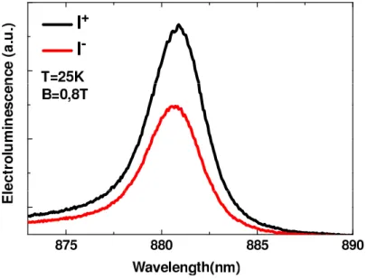
1.12 Typical electroluminescence spectra for a Spin-LED at 25K for I+ and
I− components (here the QW embedded in the spin-LED is a 10 nm
thick In0.1Ga0.9As/GaAs QW). . . . 32
1.13 Magnetic field dependence of the EL circular polarization PEL [(a) and
(b)] (raw data) and PC [(c) and (d)] (after substraction of the spurious
signal increasing linearly with the applied magnetic field) for spin-LED I (8% of Al) at 100 K and spin-LED II (16% of Al) at 290 K (open
circles). The crosses in (a) are the PEL of a control sample with a Pt
electrode. The solid lines in (c) and (d) show the field dependence of the
CoFe moment measured with a SQUID magnetometer at 20 K, which has been scaled to allow comparison with PC. [9] . . . 34
LIST OF FIGURES xv
1.14 Dispersion curves E(k2) at k∥ = 0 for MgO (001). k and k∥ are repec-tively the normal (z axis) and in-plane components (with respect to the
MgO layer) of the vector k. k2 is given in units of ∆z−1, with ∆z cor-responding to the interplanar spacing in MgO. The energy is given in
Hartree (1 Hartree=27,2 eV). The region of interest is within the en-ergy gap of MgO at the Fermi level EF. The values of k2 are negative
(k2 = (iλ)2), corresponding to evanescent wavefunctions of the type Ψ(z) = Aexp(−2λz). [10] . . . 35
2.1 Time Resolved Photoluminescence Spectroscopy Setup . . . 41
2.2 (a) Operation principle of the streak camera; (b) Sketch of the sweeping
mechanism responsible for the time resolution; (c) Spectral sensitivity of the photocathodes . . . 43
2.3 An example of image obtained with a streak camera . . . 43
2.4 Polarization Resolved Electroluminescence Spectroscopy Set-up . . . . 46
2.5 Polarized Photoluminescence Excitation Spectroscopy Set-up . . . 48
3.1 Spin-LED structure with a single InGaAs/GaAs quantum well. The CoFeB/MgO/GaAs tri-layers is decomposed in terms of a top interface
CoFeB/MgO and a bottom interface MgO/GaAs . . . 56
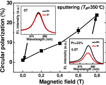
3.2 Spin-LED (annealed at 350◦C) with a sputtered tunnel barrier at T=25
K. EL Circular polarization as a function of the applied longitudinal
magnetic field. Top inset: EL spectra at 25 K at zero magnetic field for
Iσ+ (thick black line) and Iσ− (thick red line) EL components. Bottom
Inset: same quantities for B=0.8 T. . . 57
3.3 Electroluminescence circular polarization PC as a function of the
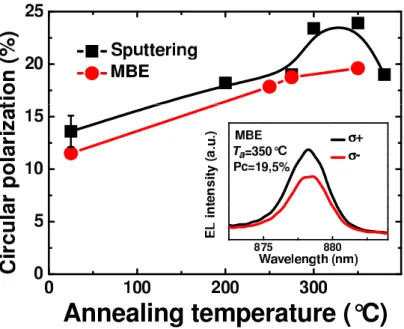
an-nealing temperature for sputtered (black squares) and MBE (red circles) grown MgO tunnel barriers. Inset: EL spectra of a Spin-LED (annealed
at 350◦C) with a MBE grown tunnel barrier at 25 K for B=0.8 T for Iσ+ (thick black line) and Iσ− (thin red line) EL components. . . . 59
3.4 PL and circular polarization measurements performed on bare p· i · n sample annealed at 350◦C at T=25 K. Top: Photoluminescence intensity
components I+and I− with respectively σ+polarization (black squares) and σ− polarization (red squares) as a function of time after a 1.5 ps
laser σ+ pulsed excitation at 780 nm (above the GaAs bandgap). The sum of the two intensity components Isum = I++ I− is displayed in
pink opened circles. The decay is characterized by the electron lifetime
τ . Bottom: time evolution of the circular polarization rate PC of the
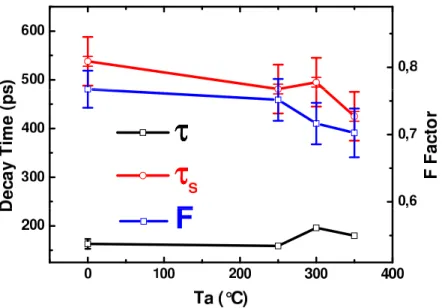
photoluminescence at T=25 K (blue line). The decay is characterized by the electron spin relaxation time τs. . . 60
3.5 Relative variation of the circular polarization (black squares) and F
fac-tor (red circles) on bare p·i·n samples annealed at different temperatures. 61
3.6 Electron spin relaxation time τs (red open circles), electron lifetime τ
(black open squares) and F factor (blue open stars) as a function of the annealing temperature TAN. . . 62
3.7 SQUID measurements. (a) Out-of-plane hysteresis curves (normalized
magnetization as a function of the applied longitudinal magnetic field) for TAN = 25◦C (black line), TAN = 275◦C (red line) and TAN = 350◦C
(green line). (b) In-plane coercitive field Hc as a function of the
an-nealing temperature TAN for a spin-LED based on a sputtered tunnel
barrier (red circles) and for a spin-LED based on a MBE grown tunnel barrier (black squares). (c) top: Spin-LED based on a MBE grown MgO
tunnel barrier. In-plane hysteresis curves (normalized magnetization as a function of the applied magnetic field) for different annealing
temper-atures TAN. Bottom: Same measurements for a Spin-LED based on a
LIST OF FIGURES xvii
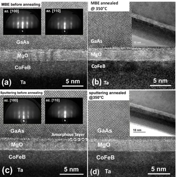
3.8 (a) HRTEM image of the sample with the MBE grown MgO tunnel barrier before annealing. Insets: RHEED images for [100] and [110]
directions (left and right insets respectively). (b) HRTEM image of the sample with the MBE grown MgO tunnel barrier after annealing at
TAN = 350◦C. Inset: TEM image at low magnification showing the good
homogeneity of the layers. (c) HRTEM image of the sample with the
sputtered MgO tunnel barrier before annealing. Upper insets: RHEED images for [100] and [110] directions (left and right insets respectively).
(d) HRTEM image of the sample with the sputtered MgO tunnel barrier after annealing at TAN = 350◦C. Inset: TEM image at low magnification
showing the good homogeneity of the layers. . . 66
3.9 Spin-LED with a sputtered tunnel barrier for TAN = 300◦C. Left panel:
EL spectra at 25 K for B=0.8 T for I+ (thick black line) and I− (thin
red line) EL components. Inset: EL Circular polarization as a function of the applied longitudinal magnetic field. Right panel.: EL spectra at
250 K for B=0.8 T for I+ (thick black line) and I− (thin red line) EL components. . . 68
3.10 (a) Spin-LED with a sputtered and a MBE grown tunnel barrier an-nealed at 300◦C. T=25 K. B=0.8 T : EL Circular polarization as a
function of the current. Inset: PC as a function of the current for
sput-tered samples at different annealing temperatures. (b) Spin-LED with
a sputtered and a MBE grown tunnel barrier annealed at 300◦C. T=25
K. B=0.8 T : EL Circular polarization as a function of ∆V = V − Vth. 69
3.11 Scheme of the principle of injection for Spin-LEDs with a sputtered (left)
and MBE grown (right) MgO tunnel barrier . . . 72
3.12 T=25 K. (a) EL intensity as a function of the current for spin-LEDs with a sputtered tunnel barrier (black squares) and a MBE grown tunnel
barrier (red squares) for TAN = 300◦C in the low current regime. (b)
EL intensity (log scale) as a function of the current for spin-LEDs with
a sputtered tunnel barrier (black squares) and a MBE grown tunnel barrier (red squares) for TAN = 300◦C. . . . 73
3.13 Central wavelength of the EL emission as a function of the injected current for a sputtered sample (black squares) and a MBE sample (red
squares) annealed at 300◦C. Top left inset: EL spectra as a function of
the current for a spin-LED with a sputtered tunnel barrier annealed at
300◦C. Bottom right inset: EL spectra as a function of the current for
a spin-LED with a MBE grown tunnel barrier annealed at 300◦C. . . . 74
3.14 T=25 K. Circular polarization as a function of the EL intensity for a
spin-LED with a sputtered tunnel barrier (black squares) and a MBE grown tunnel barrier (red squares) for TAN = 300◦C. . . . 75
3.15 Left: schematic device structure of a spin-LED. Right: HRTEM image of
CoFeB/MgO PMA injector; Inset of HRTEM image: low magnification image showing the excellent homogeneity and the low roughness of the
structures. . . 77
3.16 Left: layer-resolved orbital moment anisotropy (∆µ). Middle: schemat-ics of the calculated crystalline structures. Fe, Mg, and O are represented
by blue, green, and red balls, respectively. Right: DOS with spin-orbit coupling for averaged Fe 3d out-of-plane (3dz2 + 3dxz + 3dyz) and
in-plane orbitals (3dx2−y2+ 3dxy) with Fe both at the interface (Fe5) and in
the bulk (Fe3). Inset: a simple picture showing that the origin of PMA
comes from the hybridization of Fe out-of-plane orbitals (3dz2, 3dxz and
3dyz) and O 2pz orbitals, which leads to an uncompensated charge
occu-pation in Fe in-plane orbitals (3dx2−y2, 3dxy) and results in an enhanced
out-of-plane orbital moment leading to PMA. . . 79
3.17 RT out-of-plane M-H curves for spin-injectors with different CoFeB
thicknesses with TAN = 250◦C. . . . 80
3.18 M-H curves at 30 K for a spin-injector with 1.2 nm of CoFeB and TAN =
LIST OF FIGURES xix
3.19 EL spectra at 25 K with zero magnetic field for the optimized PMA conditions sample for σ+ and σ− polarizations when the field is swept
from positive to negative values (curves on the top) and from negative to positive values (curves on the bottom) in the hysteresis loop . . . 82
3.20 PC as a function of the out-of-plane magnetic field measured at 25 K for
a spin-LED with 1.2 nm CoFeB/MgO injectors, which is compared to
the corresponding out-of-plane M-H hysteresis loop at 30 K by SQUID in PMA optimized conditions. . . 82
3.21 (a) PC as a function of out-of-plane magnetic field measured at 25 K for
the spin-LED with optimized PMA injector with a bias of 2.3 V. (b-i) EL spectra for σ+and σ− components at different magnetic field, which
are indicated in the hysteresis loop in (a). . . 83
3.22 MCD measurement from the PMA spin-LED as a function of magnetic
field at 25 K. PC of the EL for a reference sample without CoFeB layer
as a function of magnetic field at 25 K. . . 84
3.23 In the as-grown injector (non annealed spin-LED), hysteresis loops from
Pc (solid line) and corresponding SQUID data (dotted line) at 30 K . . 85
3.24 PC as a function of the out-of-plane magnetic field measured at 300 K for
the spin-LED with optimized PMA injector, which is compared to the
out of plane M-H hysteresis loop at 300 K measured by SQUID. Inset: EL spectra at 300 K with zero magnetic field for σ+ and σ− polarizations. 86
3.25 (a) PC as a function of the out-of-plane magnetic field measured at 300
K for the spin-LED with the optimized PMA injector at a bias of 2.3 V.
(b-i) EL spectra for σ+ and σ− components at different magnetic fields,
which are indicated in the hysteresis loop in (a). . . 86
3.26 Temperature dependence of PC without magnetic field and with a 0.4 T
field. The temperature dependence of Psis calculated using: Ps = PC/F
3.27 Typical PL spectra after integration in time domain for σ+ and σ− components. Pc is deduced from (Iσ+− Iσ−)/(Iσ++ Iσ−). . . 88
3.28 Left: PL intensity (color code in arbitrary units) as a function of both time and photon wavelength. The white curve represents the PL
in-tensity as a function of time when the emission is spectrally integrated. Right: PL circular polarization degree PC (color code from PC = 0 to
PC = 44% ) as a function of both time and photon wavelength. The
white curve represents PC as a function of time when the emission is
spectrally integrated. . . 89
3.29 Determination of the carrier lifetime τ from an exponential fit of the decay time of the PL intensity (Iσ++ Iσ−). . . . 89
3.30 Determination of the spin lifetime τs from an exponential fit of the decay
time of the normalized PC. . . 90
3.31 Temperature dependence of the electron lifetime τ , the electron spin relaxation time τs and the F factor in the QW. . . 90
3.32 PC as a function of applied bias for the optimized PMA condition
sam-ple. Inset: EL spectra at 25 K with zero magnetic field for σ+ and σ− polarizations under a bias of 2.34 V. . . 91
4.1 Schematics of the GaAs band structure; the arrows present the optical excitations Eexc = 2.987eV and detection energies used in the
experi-ments of the following section. The high symmetry points in this figure are labelled according to [11]. . . 99
4.2 Reflectivity of etched GaAs at 80 K [12] . . . 99
4.3 Spin relaxation time in the Γ valley and longitudinal spin relaxation
time in the L valley as a function of temperature for a non-degenerate electron gas. The collision time is taken as τp = 200f s. . . 102
LIST OF FIGURES xxi
4.5 Dependence of the degree of circular polarization of the luminescence in GaAs on the exciting photon energy [13] . . . 103
4.6 Time-integrated photoluminescence spectrum and the corresponding
cir-cular polarization following a σ+-polarized laser excitation at an energy
Eexc = 2.987 eV. . . 105
4.7 PL circular polarization as a function of the excitation energy at 10K.
Inset: photogenerated electron spin polarization calculated using LDA and k· p band structures. . . 106 4.8 Photoemission spectrum of spin polarization from GaAs+CsOCs at low
temperature. [14] . . . 107
4.9 Selection rules in L-valleys . . . 108
4.10 Sketch of the Brillouin zone of GaAs displaying the eight L valleys. Note that two L-valleys differing by a translation of the reciprocal lattice are
equivalent. The blue arrows represent the photogenerated spins in L valleys. . . 108
4.11 Variation of the PL circular polarization degree as a function of the
transverse magnetic field B. The full line is a Lorentzian curve with TS
= 140 ps. . . 110
4.12 Time evolution of the PL circular components I+ and I−, and the
cor-responding circular polarization Pc for a near band-gap excitation. . . . 112
4.13 Schematic representation of the two-level model including the spin re-laxation times in both L and Γ valleys . . . 113
5.1 Band gap energies and spin-orbit split-off energy calculated using the
BAC model [15] . . . 140
5.2 band gap energies and spin-orbit split-off energy calculated using tight-binding model [16] . . . 141
5.3 PL peak emission energy (a) and FWHM (b) plotted as a function of temperature for the as-grown sample excited at 1 mW (filled squares)
and 10 mW (filled triangles), and for the 750◦C annealed sample at 1
mW (empty squares) and 10 mW (empty triangles). . . 144
5.4 Time integrated PL spectra for the as-grown and annealed samples at
750◦C, taken at room temperature and 1 mw excitation power . . . 145
5.5 Arrhenius plots for the as-grown sample (empty circles) and the annealed
(crosses) sample at 1 mW. The dashed lines represent the fitting lines for the calculation of the defects’ activation energies in the annealed sample. 146
5.6 TRPL curves for the as-grown sample (a) and the annealed sample (b), taken at 1 mW incident power for a series of increasing temperatures up
to 300 K. (NB: The amplitudes of the signals in the two graphs are not comparable as data were taken under different acquisition conditions.)
Spectra are shifted for presenting more clearly. . . 147
5.7 Decay time plot versus temperature for the as-grown (filled squares) and 750◦C annealed samples (empty circles) at 1 mW incident power. The
normalized TRPL curves taken at 10 K are shown in the inset (stacked for clarity), together with the exponential fit for the annealed sample. . 148
5.8 Co-polarized I+(black line) and counter-polarized I−(red line) PL com-ponents, and related circular polarization degree (Pc) at room
tempera-ture under circular (black squares) or linear (hollow squares) excitation; dashed lines are guides to the eye. . . 150
5.9 Time dependence of the PL circular polarization degree for B=0T (black
hollow squares) and B=0.73T (red hollow squares) at T=100 K, the black exponential decay line is a guide to the eye. The inset shows the
measured Larmor precession frequency µ = Ω/2π as a function of the applied magnetic field. . . 151
5.10 Measured electron g-factor in GaAsBi (black squares) as a function of lattice temperature with respective error bars, the line is a guide to the
eye. The inset shows an example of acquired TRPL spectrum (I+ com-ponent) with clear intensity oscillations appearing after the application
of a transverse magnetic field of 0.73 T. . . 152
5.11 The principle of spin quantum-beat dephasing measurements. The sign of the dephasing between the +B and -B experiments allows one to
determine the electron transverse Land´e g factor sign. [17] . . . 153
5.12 Luminescence polarization oscillations at T=100 K for the GaAsBi (main graph) and GaAs (inset) transitions, showing the temporal phase shift
∆t between positive (B−→ex, black hollow squares) and negative (-B−→ex,
red hollow circles) external magnetic field. . . 154
5.13 Experimentally measured electron spin relaxation time in intrinsic GaAsBi
as a function of temperature (blue circles), plotted within the theoret-ically expected values calculated by Tong et. al. with a photo-electron
density of 1017cm3. . . 155
Introduction
The degree of freedom associated to the electron spin plays nowadays a key role in devices (e.g. Magnetic tunnel junctions) based on ferromagnetic metals, which is the
crowning achievement of spin electronics or spintronics [18], a research field symbol-ized by the discovery of the Giant Magnetoresistance in 1988 [19,20] (by A Fert an
P. Gr¨unberg, Nobel Prize laureates in 2007). In parallel, the electron spin properties in semiconductors have been explored since the sixties [21,22], mainly by the
orien-tated optical pumping technique. Since the middle of the nineties, the idea to use the electron spin in devices based on semiconductors (that will present the advantage
of a very accurate control of the charge compared to metals) is the field of intense research in the United States [23], Europe [24] and Japan [25]. New components
char-acterized by low power consumption and higher speed or new functionalities (Spin transistors [26], spin Light Emitting diodes (Spin-LEDs) [27], spinLasers [28]) have
been proposed in the past decade. The semiconductor spintronics challenges are spin current generation [29] (and in particular electrical injection) and transport, spin
stor-age and manipulation [26] (in view of the quantum treatment of information [30]), and spin current detection. A part of spintronic development in semiconductors is devoted
to group IV semiconductors as Silicon and Germanium [31,32], but we concentrate in this thesis on spin injection into III-V semiconductors in view of spin-optoelectronics
applications. This thesis is focused on two of the previous cited challenges: electrical spin injection into III-V semiconductors and exploration of spin properties of new
ma-terials as GaAsBi in view of manipulation of spin carriers.
The first axis of this work is devoted to electrical spin injection in hybrid
Ferromag-netic Metal/Semiconductor nanostructures (FM/SC). Among all the methods consid-ered in order to generate spin polarized currents in a semiconductor [29], the efficient
electrical injection of spin polarized electrons from a ferromagnetic metal towards a semiconductor could constitute a key step in view of realization of semiconductor
de-vices with new functionalities based on the spin. In addition to the extrinsic spin relaxation processes due to the structural quality of the interfaces, the large difference
of conductivity between these two materials has been identified as a fundamental obsta-cle to the spin injection, that can be overcome by the insertion of a thin tunnel barrier
at the interface FM/SC. As injectors based on crystalline MgO tunnel barriers have exhibited up to now the highest spin injection efficiencies into III-V semiconductors, we
have focused our work on CoFeB/MgO electrodes. A powerful way to study the pro-cesses that govern the spin injection and its efficiency through an interface is to probe
the electron spin polarisation by analysing the circular polarization degree of the elec-troluminescence (EL) emitted in the semiconductor part of the Spin-LEDs [27,33,34].
This method relies on the exploitation of the optical selection rules that govern the radiative recombination of carriers in semiconductor heterostructures.
Using Spin-LEDs based on InGaAs quantum wells, we have analysed the influence of the growth technique (Molecular Beam Epitaxy or Sputtering) of the MgO layer on
the efficiency of the spin injection process. Combined analysis of polarization-resolved electroluminescence with time-resolved photoluminescence (TRPL), transmission
elec-tron microscopy (TEM) and superconducting quantum interference device (SQUID) magnetometer measurements, lead to the conclusion that the control of the quality
of the CoFeB/MgO interface is more important than the one of MgO/GaAs interface for an optimal spin injection. A systematic study of the impact of the post-annealing
temperature of the injector is also performed for the two types of samples. Both show the same trend: an increase of the EL circular polarization (PC) when the annealing
temperature TAN increases, with an optimized temperature in the range 300− 350◦C.
We attribute this behavior mainly to the improvement of the chemical structure at
the top CoFeB/MgO interface. The current dependence of the electrical spin injection is also investigated for samples prepared by the two growth techniques. We
demon-strate that the electroluminescence circular polarization is very stable as a function of the injected current for sputtered tunnel barriers, whereas this polarization decreases
abruptly when the current increases for tunnel barriers grown by Molecular Beam Epi-taxy. We attribute this behavior to the MgO/GaAs interface that presents specific
Introduction 3
characteristics depending on the growth method. It appears that in view of future applications, spin-LEDs with sputtered tunnel barriers present the best compromise
between high electroluminescence circular polarization and high electroluminescence intensity. Finally we have demonstrated a very efficient electrical spin injection
with-out any external magnetic field using an ultrathin (a few monolayers thick) CoFeB injector that presents Perpendicular Magnetic Anisotropy (PMA). The EL circular
polarization rate PC can reach values as large as 20% at 25 K, which is more than
six times the values obtained with usual multilayer PMA injectors [35] up to now. A
significant PC (∼ 8%) is conserved at room temperature. A systematic study of PC
as a function of temperature leads to the conclusion that the injection is stable with
temperature and that the variation of PC are due to variation of the electron lifetime
and spin relaxation times within the quantum well.
In a second part, we have explored the electron spin properties in the L valleys in GaAs, by polarisation-resolved Photoluminescence Excitation (PLE) spectroscopy in
the blue range. These high energy electrons might play an important role in devices based on spin transport (as for example, if one wants to observe the recently predicted
spin Gunn effect [36]) as well as in devices where electrical spin injection of high kinetic energy electrons occurs [37]. We demonstrate that a significant fraction of the electron
spin memory can be conserved when the electron is scattered from the L to the Γ valley despite an energy relaxation of several hundreds of meV. The dependence of the circular
polarization rate measured in Γ as a function of the laser energy is in good agreement with LDA and k.p calculations. Combining high energy photoexcitation experiments
under transverse magnetic field (Hanle curves) with time-resolved photoluminescence spectroscopy of Γ valley spin-polarized photogenerated electrons allows us to deduce a
typical L-valley electron spin relaxation time of 200 fs, in agreement with theoretical calculations where large spin splitting of conduction bands are expected for these
val-leys [38].
In the last part, the spin properties of GaAsBi as a potential new material for
spin-tronics are explored. The electron spin relaxation time is measured by polarization-resolved TPRL and suggests a diminution of the effective mass of conduction electrons.
The measurement of Land´e g factors are performed by TRPL under transverse mag-netic field by analysing the period of spin quantum beats as a function of the magmag-netic
field. A significant increase of the Land´e g factor compared to the one of GaAs is observed, due to the decrease of the bandgap and the increase of the spin–orbit
in-teraction in GaAsBi. Note that large g-factors and strong spin orbit coupling could present an interest for spin manipulation by external magnetic field and electric field
respectively. The investigation of the spin properties of GaAsBi under circularly po-larized light constitutes an interesting way to probe the electronic properties of this
material. It appears that the introduction of Bismuth into GaAs strongly modifies the band structure, not only in the valence band, but also in the conduction band. Further
investigations of the influence of the composition of Bi in GaAsBi should be led in order to have a deeper understanding of these modifications, and to be able to tune
the optical properties of this material that could present also a potential interest for Photovoltaic and optical telecommunications applications.
This manuscript is divided into five chapters. In the first chapter we recall the main characteristics of the band structure of bulk III-V semiconductors. We briefly
present the principle of the envelope function theory that allows to calculate the con-fined energy levels in heterostructures as quantum wells. Optical selections rules in
the centre of the Brillouin zone, as well as the principle of spin relaxation mechanisms, are presented. A short introduction to the problematic of electrical spin injection is
given, and the obstacle of “conductivity mismatch” between ferromagnetic metals and semiconductors is evoked. The principle of optical detection of electrical spin
injec-tion by the use of spin-LEDs is explained. The second chapter of the manuscript is devoted to the description of experimental set-ups of optical spectroscopy employed
in this thesis (Electroluminescence and Ultra-fast Time-Resolved Photoluminescence at the picosecond timescale). A specific set-up of high sensitivity polarisation-resolved
Photoluminescence Excitation (PLE) spectroscopy based on a double modulation tech-nique has been developed in order to study electrons spin properties in the L valleys of
GaAs. In chapter 3 we tackle the problem of electrical spin injection into GaAs with crystalline MgO tunnel barriers. We analyse the influence of the growth technique of
the MgO layer as well as the influence of the current injected in the spin-LEDs on the spin injection efficiency. Finally, electrical spin injection without any external magnetic
field using an ultrathin CoFeB layer is demonstrated up to room temperature. Chap-ter 4 is devoted to the electron spin properties in the L valleys (in particular the spin
Introduction 5
relaxation time) of GaAs, studied by polarisation-resolved Photoluminescence Excita-tion (PLE) spectroscopy in the blue range. To finish with, in chapter 5 the potential
of GaAsBi as a new material for spintronics, as well as its band structure modification due to Bi inclusion are explored by measuring spin relaxation times and Land´e g-factors.
Chapter 1
Introduction to the electronic and
optical properties of zinc blende
III-V semiconductors
1.1 III-V semiconductors band structure . . . . 9
1.1.1 Bulk semiconductors . . . 9 1.1.2 Semiconductor heterostructures . . . 12
1.2 Optical orientation in zinc-blende semiconductors . . . . . 17
1.2.1 Optical transitions . . . 17 1.2.2 Optical selection rules . . . 18
1.3 Main spin relaxation mechanisms . . . . 21
1.3.1 D’Yakonov-Perel Mechanism . . . 21 1.3.2 Elliott-Yafet Mechanism . . . 22 1.3.3 Bir-Aronov-Pikus Mechanism . . . 23 1.3.4 Electron spin relaxation due to the Hyperfine-interaction . . 23 1.3.5 Exciton spin relaxation mechanism . . . 24
1.4 Electrical spin injection into Spin-LEDs . . . . 24
1.4.1 Problem of impedance mismatch in the diffusive regime . . . 25 1.4.2 Spin Light Emitting diodes as a tool to detect and quantify
electrical spin injection . . . 30 1.4.3 State of the art: breakthrough due to MgO tunnel barriers . 33
In this chapter we present the basic physics in the bulk semiconductors and
semicon-ductor heterostructures. In the first part, we discuss the electronic band structure at the center of the Brillouin zone of III-V semiconductors. We will present the electronic
properties in quantum wells. Then, in the second part, we detail the fundamental principles of optical selection rules. The third section is devoted to spin relaxation
mechanisms. After having presented the main electronic and spin properties of III-V semiconductors bulk and heterostructures, we give in the last section a short
intro-duction to the problem of the electrical spin injection from a ferromagnetic electrode into a semiconductor through a tunnel barrier, a problem that will be at the heart of
chapter 3. The principle of the optical detection of this spin injection process by the use of a Spin Light Emitting Diode is also presented.
1.1. III-V semiconductors band structure 9
1.1
III-V semiconductors band structure
1.1.1
Bulk semiconductors
In this section, we present the main characteristics of the band structure of zinc
blende semiconductors. As shown in Figure 1.1, in zinc blende structure (like GaAs, InP, etc. ) each atom’s nearest neighbors consist of four atoms of the opposite type.
The two types of atoms interpenetrate face-centered cubic lattices. The lattice param-eter a is the edge length of the cube.
The Hamiltonian of an electron in a crystal periodic potential V (r) can be described
Figure 1.1: Schematic representation of the zinc blende structure.
as:
H = −¯h 2
2m0
∆r+ V (⃗r) (1.1)
m0 is the electron mass in vacuum. The eigenstate ψ of Hamiltonian of equation 1.1
can be written as:
ψ(⃗r) = u(⃗r)ei⃗k⃗r (1.2)
where ⃗k is the wave vector and u(⃗r) has the same periodicity as the crystal potential.
The electron eigenenergies are divided into conduction band and valence band. The electronic state at ⃗k = 0 corresponding to the conduction band is denoted |S⟩ due to its spherical symmetry, while the degenerate solutions of the valence bands are noted
Taking into account the electron spin and the orbital angular momentum interaction, we get a supplementary term Wso in the crystal Hamiltonian H0,
H = H0+ Wso = p2 2m0 + V (⃗r) + h¯ 4m2 0c2 σ· (∆V (⃗r) × p) (1.3) where σ is Pauli matrix. The third term in Equation 1.3 can be converted into the
following form in spherical symmetry:
¯ h 4m2 0c2 σ· (∆V (⃗r) × p) = ¯h 2m2 0c2 1 ⃗r dV dr(⃗L· ⃗S) (1.4)
where L is the orbital angular momentum, S is the spin angular momentum (±1/2), J is the total angular momentum (J = L + S). The conduction band is separated from
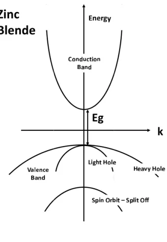
the valence band (VB) by a bandgap energy Eg. (As shown in Figure 1.2). The valence
band is then separated into a group of two double degenerate bands: heavy hole (HH)
and light hole (LH), and a band called split-off (SO) which is separated from the two other bands by the spin-orbit coupling energy ∆so. In GaAs, ∆sois 341 meV at 300 K.
The conduction states at k = 0 can be described in the base |S ↑⟩ and |S ↓⟩ which correspond to the eigenvalue Ec. The valence bands’ states at k = 0, which corresponds
to the eigenvalue Ev, are described the bases |X ↑⟩, |X ↓⟩, |Y ↑⟩, |Y ↓⟩, |Z ↑⟩, and
|Z ↓⟩ (here the sign ↑ and ↓ represent the spin angular momentum).
Table 1.1 summarized the eigenfunctions and eigenenergies in this base. Conduction
Eigenfunction ui ’Atomic’ notations Eigenenergies
un |J, mj⟩ u1 =|S, ↑⟩ |12,12⟩ Ec= EHH + EG u2 =|S, ↓⟩ |12,−12⟩ u3 = 1 √ 2|(X + iY ), ↑⟩ | 3 2, 3 2⟩ Ev= EHH u4= 1 √ 2|(X − iY ), ↓⟩ | 3 2,− 3 2⟩ u5= 1 √ 6|(X + iY ), ↓⟩ − √ 2 3|Z, ↑⟩ | 3 2, 1 2⟩ Ev= ELH = EHH u6=− 1 √ 6|(X − iY ), ↑⟩ − √ 2 3|Z, ↓⟩ | 3 2,− 1 2⟩ u7= 1 √ 3|(X + iY ), ↓⟩ + √ 1 3|Z, ↑⟩ | 1 2, 1 2⟩ Eso = EHH − ∆so u8=− 1 √ 3|(X − iY ), ↑⟩ + √ 1 3|Z, ↑⟩ | 1 2,− 1 2⟩
Table 1.1: Bloch eigenfunctions at the zone centre for a zinc-blende semiconductor
1.1. III-V semiconductors band structure 11
holes and light holes are u3, u4 and u5, u6 respectively. u7, u8 are the split-off bands.
For calculating the band structure at ⃗k ̸= 0, the k · p method can be used. By substituting the Bloch function into Schr¨odinger equation, we obtain:
( p 2 2m0 + V (⃗r) +h¯ 2k2 2m0 +hk¯ · p m0 )un,k(⃗r) = En,kun,k(⃗r) (1.5)
Where the energies En,k=0 are considered known. The k · p method consists in
treating the ¯hk· p operator as a pertubation to the Hamiltonian and, by considering
a small variation of the k vector from the central zone, the eigenenergies at k̸= 0 can be calculated as: En,k = En,0+ ¯ h2k2 2m0 + ¯h 2 m2 0 ∑ m̸=n |⟨un,0|k · p| um,0⟩| 2 En0− Em0 (1.6)
The band structure of zinc blende semiconductors near the center of Brillouin zone
calculated according to the k· p method in first approximation is presented in Figure 1.2, the energies show a parabolic dispersion.
In order to describe more precisely the degenerate valence bands, Luttinger-Kohn
model [39,40] can be used in which the coupling between two degenerate conduction bands is neglected and the L¨owdin partitioning method [41] is employed to treat the
six degenerate valence bands. The general Hamiltonian for both cases of light and heavy holes are written as :
HL= ¯ h2 2m0 [(γ1+ 5 2γ2)∇ 2− 2γ 3(∇ · J)2 + 2(γ3− γ2)(∇2xJ 2 x+ c.p.)] (1.7)
where γ1, γ2, γ3are Luttinger parameters determined by experiments [42], J = (Jx, Jy, Jz)
is total angular momentum operator, c.p. stands for cyclic permutation [43]. The
eigenenergies of both light and heavy hole states are found in terms of Luttinger pa-rameters, E(k) = Ev(0) + ¯ h2 m0 [γ1k2± 2 √ γ2k4+ 3(γ32− γ22)(kx2ky2+ k2ykz2+ k2zk2x)] (1.8)
Intuitively, equation 1.8 shows that heavy holes (positive sign) and light holes
(nega-tive sign) are degenerated at ⃗k = 0 and split for ⃗k ̸= 0 into two subbands with different characteristics presented by different effective masses. In fact, the relationship between
the effective masses of heavy and light holes of (100) equivalent direction can be ex-pressed in the forms related to Luttinger parameters :
m∗hh m0 = 1 γ1− 2γ2 m∗lh m0 = 1 γ1+ 2γ2
For GaAs, the values of the Luttinger parameters are γ1 = 7.0, γ2 = 2.25, γ3 = 2.9
[43,44].
1.1.2
Semiconductor heterostructures
An heterostructure is composed of different layers of dissimilar crystalline semicon-ductors with unequal bandgap energies. In practice, advanced epitaxial techniques
such as Molecular Beam Epitaxy (MBE) or Metal-Organic Chemical Vapor Deposition (MOCVD) allow us to grow layers as thin as a few atomic layers, in which the motion
1.1. III-V semiconductors band structure 13
of carriers is quantized. The heterostructural interfaces play a critical role in semicon-ductor heterostructure devices such as field-effect transistor (FET), bipolar transistor,
light-emitting diode (LED), laser,... etc because they exhibit many interesting and useful electronic properties associated with their discontinuities of band structure at
their interfaces [45]. This section recalls some basis on semiconductor heterostructures.
Envelope function approximation
As discussed before, the Bloch function only describes electron wavefunction under crystal periodic potential. However, in semiconductor heterostructure, the periodic
condition is broken because of the interface between two different materials. In this situation, envelope function approximation (EFA) is implemented to find the
wave-function of electron in semiconductor heterostructures.
The Schr¨odinger equation for semiconductor heterostructures is written as [1]:
(−¯h
2
2m0
∆r+ Vc(⃗r) + Vh(⃗r))ψnk(⃗r) = Enkψnk(⃗r) (1.9)
where n is band index, m0 is the free electron effective mass, Vc(⃗r) is the crystal
po-tential, Vh(⃗r) is the heterojunction intefacial potential. In EFA method, the interfacial
potential Vh(⃗r) is considered as a pertubative component. In fact, the EFA method
is valid under two assumed conditions : the envelope wavefunction and the density of current probability are continuous through the interface. Now the wavefunction of an
electron in semiconductor heterostructure is found in this form :
ψn,k(⃗r) = Fnk(⃗r)un0(⃗r)
where Fnk(⃗r) is the envelope function and un0(⃗r) is the Bloch wavefunction at k = 0.
The equation 1.9 becomes :
( −¯h
2
2mc(⃗r)
∆r+ Vh(⃗r))Fnj(⃗r) = (Eni− En0)Fnj(⃗r) (1.10)
where mc(⃗r) is the effective mass depending on semiconductor materials and Enj−En0
is the confinement energy. In this approximation, the heterostructure is considered as a crystal with small pertubative potential Vh(⃗r).
Electronic properties of semiconductor quantum wells
A Quantum Well (QW) is a thin layer of semiconductor structure sandwiched be-tween two layers of another semiconductor. Semiconductor quantum wells can be
divided into two categories : type I and type II [46]. We only concentrate on studying type I quantum well (for instance AlGaAs/GaAs) in which, the material of barrier
layers has wider bandgap than the quantum well layer as depicted in figure 1.3.
Figure 1.3: Schematic of band energy structure of type I quantum well [2]
Quantum well
For the band calculation, the potential for the finite quantum well is defined as :
V (z) = 0 for |z| ≤ L/2 V0 for |z| > L/2
We denote material A for quantum well layer and material B for the barrier layers.
Concerning the envelope wavefunction Φ(z), the Schrodinger equation can be written as : [Es+ Vs(z)− ¯ h2 2µ(z)( ∂2 ∂z2 + k⊥2)]Φ(z) = EΦ(z) (1.11)
where Es is the conduction band edge in the quantum well which can be set as zero
for the sake of simplicity, Vs(z) is zero in the quantum well and equals to V0 in the
1.1. III-V semiconductors band structure 15
in the barrier, k⊥ is the in-plane wavevector (k⊥2 = k2x+ ky2), Φ(z) is the z-dependent part of the envelope function.
The boundary conditions are proposed in Ben Daniel-Duke model [1,47] as follow :
ΦA(± L 2) = ΦB(± L 2) (1.12) and : 1 m∗A dΦ(z) dz |z=±L/2= 1 m∗B dΦ(z) dz |z=±L/2 (1.13)
Due to the potential symmetry, the wavefunction of a particle in this kind of quantum
well can be expressed by even and odd functions. Solving the above Schrodinger equation 1.11, the envelope wavefunction is obtained :
Φ(z) = Aeβz for z <-L/2
B cos(αz) for |z| ≤ L/2 (even states)
B sin(αz) for |z| ≤ L/2 (odd states)
Ae−βz for z > L/2 where : α = √ 2m∗A ¯ h2 En− k 2 ⊥ (1.14) β = √ 2m∗B ¯ h2 (V0− En) + k 2 ⊥ (1.15)
and A, B are normalization constants. In the case of an infinite quantum well, the associated eigenenergies are of this form :
En(k⊥) = ¯ h2 m∗A(( nπ L ) 2 + k2⊥) (1.16)
As for the bulk materials, the valence band is of more complicated treatment than the
conduction band. The approach is to add a confinement potential in Luttinger-Kohn Hamiltonian. We can rebuild the hole Hamiltonian in the QW by referring to equation
1.7 Firstly, the confinement potential term V(z) should be added into the Hamiltonian; then, the cubic term in equation 1.8 which is proportional to (γ2
3 − γ22) is rather small
in most zinc-blende semiconductors and we can omit it in a first approach. Finally, we assum that the Luttinger parameters are identical in the QW and the barriers. With
those simplifications, the Hamiltonian of holes in QW becomes : HQW = ¯ h2 2m0 [(γ1+ 5 2γ2)∇ 2− 2γ 3(∇ · J)2] + V (z)
With the assumption that Schr¨odinger function is separable in the direction of quantization from the in-plane movement, the Hamiltonian for the motion in z-direction
can be simplified in this form :
Hz = ¯ h2 2m0 [(γ1+ 5 2γ2)− 2γ3∇J 2 z]( ∂ ∂z) 2 + V (z)
Figure 1.4 illustrates the schematic of hole dispersion relation in a typical 10 nm
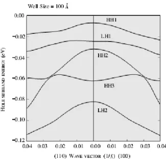
Figure 1.4: Hole relation dispersion in a 100˚A GaAs/Al0.3Ga0.7As quantum well [3]
thick GaAs/AlGaAs quantum well. As shown in this figure, the heavy hole (HH) sub-band is above the light hole (LH) subsub-band at zone center because the confinement
energy is inversely proportional to the effective mass (equation 1.16). As a result, the exciton E1-HH1 is dominant in the photoluminescence spectroscopy of type I quantum
1.2. Optical orientation in zinc-blende semiconductors 17
1.2
Optical orientation in zinc-blende
semiconduc-tors
Optical properties provide an important tool for studying many inner physical
phe-nomena in the solid. In fact, optical spectra reveal many information about electronic properties in a semiconductor such as the energy band diagram, the impurity level,
the existance of localized states, the exciton energy, etc. Optics is also very useful to study the spin properties of carriers in semiconductors. This section mentions some
background of optical orientation in zinc-blende semiconductors.
1.2.1
Optical transitions
When electromagnetic waves interact with a direct bandgap semiconductor that
has a bandgap smaller than photon energy, electrons in the lower energy states are excited to higher energy states following the energy and momentum conservation laws
and making an optical transition. There are different kinds of optical transitions in semiconductor. Interband transitions take place between the conduction band and the
valence band, in which electrons in the occupied states of the valence band are excited in the empty states of the conduction band. Intraband transitions happen inside one
band (the conduction band or the valence band) and involve only one type of carrier (electron or hole).
An electromagnetic radiation can be described by its electric field E(r, t) and mag-⃗
netic field H(r, t) equivalent to a vector potential⃗ A(r, t) which is defined as:⃗
⃗ E(r, t) = −1 c∇ · ⃗ A(r, t) ⃗ H(r, t) = ∇ ×A(r, t)⃗
The Hamiltonian of an electron in the presence of an electromagnetic field is written
as : H = 1 2m0 (p−eA c ) 2+ V (r) (1.17)
This Hamiltonian can be developped as : H = H0− e m0 ⃗ A.⃗p + e 2 2m0c A2 where H0 = p 2 2m0 + V (r). If the term of A
2 is neglected in the first approximation,
the interaction Hamiltonian between an electron and an electromagnetic field can be
written as : Hint =− e m0c ⃗ A.⃗p (1.18)
where e is electron charge, m0 is electron mass, c is the light velocity.
Using the first-order time-dependent pertubation theory, the Fermi Golden Rule states that the transition rate of an electron from an initial state |i⟩ with an energy
Ei to a final state |f⟩ with an energy Ef by absorbing a photon with the energy ¯hω is
defined as : Wif = 2π ¯ h |⟨i|Hint|f⟩| 2 δ(Ef − Ei− ¯hω) (1.19)
where Mif =|⟨i|Hint|f⟩|
2
is denoted as the transition matrix element [48] whose values determine the allowed transitions and their relative intensities; this defines the optical
selection rule. The Dirac function δ is responsible for energy conservation law in these transitions.
If the quantum states |i⟩ and |f⟩ are partially occupied, the transition probability is weighted by the occupancy factor given by the Fermi-Dirac distribution as follows:
Ri→f = Wiff (Ei)[1− f(Ef)] (1.20)
where f (E) = (1 + ekB T1 (E−µ))−1 is the Fermi-Dirac distribution, in which kB is the Boltzmann constant, T is the temperature and µ is the chemical potential of the electron.
1.2.2
Optical selection rules
For direct bandgap semiconductors such as GaAs and InAs, the lowest energy point
in the conduction band and the highest energy point in the valence band have the same momentum at the Γ-point (k=0). Hence, interband transitions in these materials can
occur without any contribution of phonons. Optical selection rules in this situation are presented as follows.
![Figure 1.3: Schematic of band energy structure of type I quantum well [2]](https://thumb-eu.123doks.com/thumbv2/123doknet/14657109.738838/41.892.219.649.392.629/figure-schematic-band-energy-structure-type-i-quantum.webp)
![Figure 1.13: Magnetic field dependence of the EL circular polarization P EL [(a) and (b)] (raw data) and P C [(c) and (d)] (after substraction of the spurious signal increasing linearly with the applied magnetic field) for LED I (8% of Al) at 100 K and spin](https://thumb-eu.123doks.com/thumbv2/123doknet/14657109.738838/61.892.229.642.454.804/magnetic-dependence-circular-polarization-substraction-spurious-increasing-linearly.webp)