HAL Id: hal-03187821
https://hal.archives-ouvertes.fr/hal-03187821
Submitted on 1 Apr 2021HAL is a multi-disciplinary open access archive for the deposit and dissemination of sci-entific research documents, whether they are pub-lished or not. The documents may come from teaching and research institutions in France or abroad, or from public or private research centers.
L’archive ouverte pluridisciplinaire HAL, est destinée au dépôt et à la diffusion de documents scientifiques de niveau recherche, publiés ou non, émanant des établissements d’enseignement et de recherche français ou étrangers, des laboratoires publics ou privés.
Reliability-driven pin assignment optimization to
improve in-orbit soft-error rate
Y Aguiar, Frédéric Wrobel, J-L Autran, P Leroux, F Saigné, V Pouget,
Antoine Touboul
To cite this version:
Y Aguiar, Frédéric Wrobel, J-L Autran, P Leroux, F Saigné, et al.. Reliability-driven pin assignment optimization to improve in-orbit soft-error rate. Microelectronics Reliability, Elsevier, 2020, 114, pp.113885. �10.1016/j.microrel.2020.113885�. �hal-03187821�
Reliability-driven pin assignment optimization to improve in-orbit soft-error rate
Y. Q. Aguiar
a,*, F. Wrobel
a, J-L. Autran
b, P. Leroux
c, F. Saigné
a, V. Pouget
aand A. D.
Touboul
a
a Institut d’Electronique et des Systèmes, University of Montpellier, Montpellier, France
b Institut Materiaux Microelectronique Nanoscience de Provence, Aix-Marseille University, Marseille, France c Advanced Integrated Sensing Lab, KU Leuven University, Leuven, Belgium
Abstract – Electronics are increasingly susceptible to energetic particle interactions within the silicon. In order to improve the circuit reliability under radiation effects, several hardening techniques have been adopted in the design flow of VLSI systems. This paper proposes a pin assignment optimization in logic gates to reduce the Single-Event Transient (SET) cross-section and improve the in-orbit soft-error rate. Signal probability propagation is used to assign the lowest probability to the most sensitive input combination of the circuit by rewiring or pin swapping. The cell optimization can reach up to 48% reduction on the soft-error rate. For the analyzed arithmetic benchmark circuits, an optimized cell netlist can achieve from 8% to 28% reduction on the SET cross-section and in-orbit soft-error rate at no cost in the circuit design area. Additionally, as the pin swapping is a layout-friendly technique, the optimization does not impact on the cell placement and it can be adopted along with other hardening techniques in the logic and physical synthesis.
1. Introduction
The reliability of electronic circuits is subject to physical failures due to the influence of the environment, such as the presence of atmospheric or space radiation [1]. The energy deposition of a single energetic particle in the sensitive areas of a circuit can lead to destructive or non-destructive failures, known as Single-Event Effects (SEE). Memory elements, such as flip-flops and SRAMs, are subject to the Single-Event Upset (SEU), i.e. the stored logic bit is flipped due to the particle hit. On the other hand, the Single-Event Transient (SET) effect is observed in logic paths as parasitic transient currents generated from a particle hit in the sensitive regions of transistors issued from combinational circuits. As SEU and SET are not destructive effects, they are also known as soft error. Due to transistor scaling, reduced logic data path and high operating frequencies, soft errors are increasingly becoming an inevitable threat even in terrestrial environment [2].
The adoption of hardening strategies is highly recommended in order to obtain a fault-tolerant and reliable system [3]. Considering the Radiation-Hardening-By-Design (RHBD) techniques, the circuit designers can apply different approaches ranging from changes on the transistor layout, as the Enclosed Layout Transistor (ELT), to circuit and system design approaches, as the Triple-Modular Redundancy (TMR) schemes and Error Correction Codes (ECC). Due to the popularity of cell-based design methodology in ASIC systems, a variety of hardening strategies have been proposed to address radiation effects early in the design flow, such as in the physical and logic synthesis of standard-cell libraries [4-9]. For instance, a cell placement algorithm to mitigate charge sharing effects and consequently to reduce multiple SETs is proposed in [6]. Also, besides improving performance metrics, gate sizing has been shown to improve the radiation robustness [7, 8].
Signal probabilities are widely used to estimate power
consumption, and to perform timing analysis [10-12]. Considering the sensitivity to SET is directly related to the layout of the circuit and its operation mode, i.e. input signals and internal states, signal probability can also be used to improve the reliability of circuits [5]. For instance, Signal Probability based Reliability Analysis (SPRA) is another efficient tool used to analyze the reliability of VLSI circuit at gate-level [13-15]. In this context, the reliability of a gate or a circuit is defined as the confidence level that the output will be functionally correct given a fault probability. Initially, SPRA methods have been focused on physical defects due to wearout mechanisms or process variability [13]. However, due to the increase interest in reducing the impact of soft error rate, some works analyzing SET have been proposed as in [14-17]. Using a SPRA algorithm, the work in [16] proposed a cell placement strategy based on the definition of bad and good pairs of logic gates referring to a measurement on how the close proximity of the standard cells would impact the circuit error rate. Similarly, [17] proposed another cell placement approach based on the signal probability and its relation to the pulse quenching effect.
In our work, signal probability is used to propose a reliability-driven pin assignment optimization based on the input dependence of SET sensitivity of logic gates. Accordingly, an SET characterization based on the cell layout and input stimuli is considered. In summary, a layout-based analysis is performed using the Monte Carlo method for the high-energy particle interaction simulations and the SET cross-section calculation [4]. Based on the SET characterization of the standard cells, pin swapping, also known as rewiring, is adopted to assign the lowest signal probability to the input pin so that the most sensitive gate input combination obtains the lowest probability of occurrence. Besides the cross-section reduction, the optimization results provide the impact on the soft error rate for single cells individually, i.e. 2-input basic logic gates and 3-input complex gates, and for some arithmetic benchmark
Cite this article as: Y. Q. Aguiar et al., "Reliability-driven pin assignment optimization to improve in-orbit soft-error rate," in Microelectronics Reliability, vol. 114, November 2020, doi: 10.1016/j.microrel.2020.113885.
circuits.
This paper is organized as follows: the pin assignment optimization to improve SET robustness is explained in Section 2; Section 3 provides the methodology of the radiation sensitivity evaluation, in which a layout-based prediction is adopted using a Monte Carlo approach; the results are presented and explored in details in Section 4; and, to conclude, Section 5 presents the final considerations and an outlook of the results.
2. Optimizing Pin Assignment for Single-Event Transients
Pin assignment is used in the logic synthesis to improve power and performance metrics in the design of VLSI circuits by taking advantage of the functional equivalence of input pins of logic gates [18-20]. Consider the NAND gate and its truth table in Fig. 1. A symmetric input relationship is observed when both input signal are not identical, i.e. A≠B: the output signal is determined whenever one of its input is in low logic level, regardless of the input pin (a or b). The interchangeable input combinations are highlighted in Fig. 1 (red rectangular). This symmetric input relationship is observed in all 2-input basic standard cell gates. As each input pin of a logic gate presents different electrical characteristics depending on the transistor network, power-driven logic synthesis assigns the input signal with lower switching activity to the pin with higher capacitance. Similarly, a timing-driven optimization can apply pin permutation between symmetric input pins such that the late-arriving signal is always connected to the input pin with the lowest intrinsic delay [18]. This process is known as rewiring or pin swapping [19-20]. Considering that cross-section of logic gates is dependent on the input stimuli, a reliability-aware synthesis can be proposed based on the cell symmetric inputs and signal probabilities to improve the vulnerability of the circuit through optimal pin assignment.
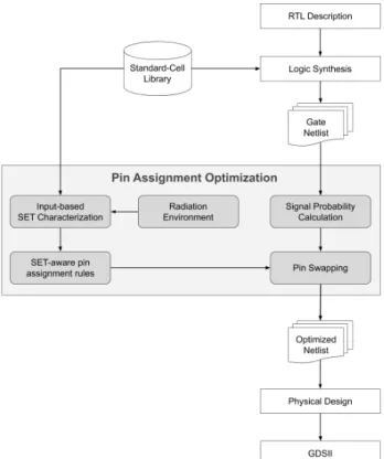
A diagram illustrating the proposed SET-aware pin assignment optimization in a cell-based circuit design flow is shown in Fig. 2. Given a circuit description in Register Transfer Level (RTL), the logic synthesis optimizes each Boolean function and maps it to logic gates available in the Standard-Cell library. As output, a gate netlist is provided, normally optimized for timing, area and/or power. With the gate netlist information and the Standard-Cell library, the SET-aware pin assignment
optimization can be performed. The first step is the Input-based
SET characterization, in which the symmetric input relationship
of each standard cell is identified and the SET cross-section for the interchangeable input combinations calculated. For instance, the cross-section for the input combination (0, 1) and (1, 0). The methodology used to calculate the SET cross-section and in-orbit rate is explained in the next section. Based on the SET characterization results, a set of pin assignment rules is defined, i.e. there will be an input pin for each standard cell in which the net with the lowest signal probability should be connected to so the most sensitive interchangeable input combination obtains the lowest probability of occurrence. The second step, considering the switching activity of the primary inputs, the signal probability calculation can be performed for the internal net connections as illustrated in Fig. 3. Based on the Boolean function of each gate, an equation is extracted to calculate the
Fig. 1. Transistor network and truth table of a 2-input NAND gate
Fig. 3. Signal probability estimation for a combinational logic circuit.
Fig. 2. SET-aware Pin Assignment Optimization in a cell-based VLSI circuit design flow.
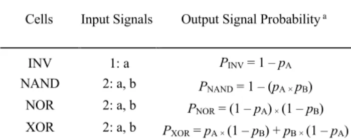
probability of the output signal to be at logic value 1, i.e. the gate output signal probability 𝑃!"#$(𝑜𝑢𝑡𝑝𝑢𝑡 = 1). In this work, the
Parker-McCluskey method [21] was used considering the primary inputs as uncorrelated and with equally switching activity of 50%, i.e. signal probability equals to 0.5. Although temporal and spatial correlation is not considered in our analysis, a more complex and accurate signal probability estimation method can be easily integrated into the development flow in Fig. 2. Applying basic probability theory, the output signal probability equations for the logic gates used in the combinational circuit in Fig. 3 are shown in Table 1. For instance, consider the inverter gate. Given the input probability 𝑝(𝑎 = 1) = 1, i.e. the signal is always at logic value 1, considering its Boolean function, the probability of the output signal to be at logic value 1 is 0 (𝑃%&'(𝑜𝑢𝑡𝑝𝑢𝑡 = 1) = 0). Thus,
the signal probability equation for the inverter is:
𝑃%&'(𝑜𝑢𝑡𝑝𝑢𝑡 = 1) = 1 − 𝑝(𝑎 = 1) (1)
For clarity, the probabilities 𝑃!"#$(𝑜𝑢𝑡𝑝𝑢𝑡 = 1), 𝑝(𝑎 =
1), 𝑝(𝑏 = 1) will be shortened to PGATE, pA and pB. Following the signal probability calculation in the Fig. 2 is the pin swapping. In this process, with the pin assignment rules and the signal probabilities, an optimization algorithm can identify which pin should be swapped in order to reduce the occurrence of the interchangeable input combination with the higher SET cross-section. After the pin swapping, the standard design flow is performed with the optimized netlist.
3. Radiation Sensitivity Methodology
In order to obtain important reliability information to be addressed in the optimization process, the SET characterization methodology is aligned to the identification of the input dependence [5]. The sensitivity of each standard cell is extracted from the layout design in the Graphical Design System (GSDII) file. Thus, the Monte Carlo simulation tool, MC-Oracle [22], is used to obtain the SET currents. In MC-Oracle, the drift-diffusion model is used for the charge collection process. Based on the SET database provided by the tool, a SET analyzer is responsible to perform the SPICE simulations and calculate the SET cross-section for each cell input combination. In order to
consider the input signal probabilities, the Eq. 2 is used. Given
n input combinations, the overall gate SET cross-section 𝜎($#
can be estimated from the input SET cross-section 𝜎($#) and the input probability p(i):
𝜎($#= / 𝜎($#)× 𝑝(𝑖) *
)+, (2)
The input cross-section 𝜎($#) is provided by the SET characterization while the input probabilities are provided by the Signal Probability Calculation in Fig. 3. Then, this equation is used in the Pin Swapping process to evaluate when the input pins assigned from the logic synthesis should be swapped to decrease the gate SET cross-section. Similarly, this process can also adopt the soft-error rate estimation for a given mission orbit. In this work, two orbits were analysed: the Geostationary (GEO) and the International Space Station (ISS) orbits. The Integral Rectangular Parallelepiped (IRPP) method is used as specified by the European Cooperation for Space Standardization (ECSS) [23]. Additionally, a fixed shielding of 1 g/cm2 is used and, under solar minimum, the international standard ISO 15390 [24] and NASA AP8MIN [25] flux models are used for the Galactic Cosmic Rays (GCR) and the trapped proton radiation. In this work, the standard cells are provided from the 45 nm OpenCell Library from NanGate [26].
4. Results and Discussions
4.1 Analysis of 2-input gates
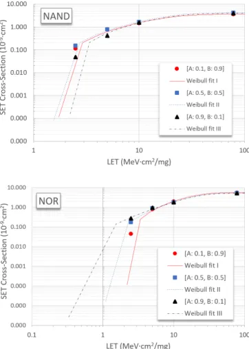
Based on the cross-section of the interchangeable input combinations, an optimized logic synthesis should prioritize the pin assignment of the lowest signal probability in such a way the most sensitive interchangeable input combination obtains the lowest probability of occurrence. The input SET cross-section for NAND, NOR and XOR gates under particle Linear Energy Transfer (LET) of 5 MeV.cm2/mg is shown in Fig. 4. It is possible to identify the most sensitive input combinations. Considering the interchangeable input, i.e. (0, 1) and (1, 0): the NAND gate is the only cell to show the lowest cross-section for the (1, 0), while the NOR and XOR gates present the (0, 1). It
Table 1
Signal Probability Estimation for the INV, NAND, NOR and XOR gates
Cells Input Signals Output Signal Probability a
INV 1: a PINV = 1 – pA
NAND 2: a, b PNAND = 1 – (pA × pB) NOR 2: a, b PNOR = (1 – pA) × (1 – pB) XOR 2: a, b PXOR = pA × (1 – pB) + pB × (1 – pA)
a Signal probability is the probability of the signal to be at logic
value 1.
Fig. 4. Input SET cross-section for the NAND, NOR and XOR gates under a particle with LET = 5 MeV.cm2/mg
implies that, considering low particle LET, the lowest signal probability be assigned to the input B for the NAND gate, and to the input A for the NOR and XOR gates.
In Fig. 5, the gate SET cross-section is calculated for the NAND and NOR gate using the Eq. 2 and considering 3 scenarios of input probabilities (Table 2 contains all the Weibull fitting parameters). Notice that, the input dependence of the SET cross-section is also dependent on the LET. It can be also observed in Fig. 6, in which the input SET cross-section is shown for 78 MeV.cm2/mg. Based on the SET cross-section
curve, we can observe that signal probability will play an important hole for low particle LET This behavior is related to the different charge collection efficiencies and the interplay relationship between pull-up and pull-down recovery dynamics. Due to this characteristic, the in-orbit rate should be analyzed to identify the best pin assignment strategy considering the complete range of particle energy present in a given mission radiation environment. This analysis is discussed later in this paper.
4.2 Analysis of 3-input gates
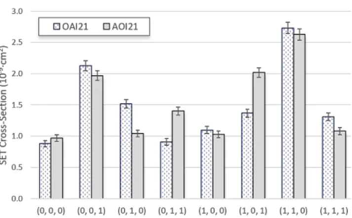
When adopting 3-input logic function such as AOI21 and OAI21, it is not possible to obtain a complete symmetric input relationship as observed for the 2-input gates. It is necessary to identify the interchangeable input combinations and the controllable input pin, i.e. the pin that controls the output of the function and the pin assignment cannot optimize it otherwise it will interfere within the correct logic function of the circuit. In Fig. 7, the transistor network and truth table of the AOI21 gate is shown. In this case, A1 is the controllable input pin while two pairs of interchangeable input combination are possible: (0, 0, 1) ↔ (0, 1, 0) and (1, 0, 1) ↔ (1, 1, 0). Analyzing the transistor network, it is possible to observe that the interchangeable input signal are the ones from the series and parallel arrangement (B1 and B2). As the OAI21 gate is the complement of the AOI21
Fig. 5. SET cross-section curves for the NAND and NOR gate in 3 input scenarios
Fig. 7. Transistor network and truth table of the AOI21 gate Table 2
Weibull fitting parameter from the cross-section curves of Fig. 5. Saturation cross-section and threshold LET correspond to Sat XS and LETTH values, respectively.
W S (10Sat XS -9 cm2) LETTH (MeV.cm2/mg) NAND I 13.74 1.16 3.57 1.73 II 14.68 1.19 4.18 1.55 III 14.84 1.15 3.94 2.22 NOR I 15.03 1.22 5.68 2.19 II 16.94 1.31 5.38 1.09 III 17.71 1.33 5.22 0.33
Fig. 6. Input SET cross-section for the NAND, NOR and XOR gates under a particle with LET = 78 MeV.cm2/mg
logic function, they present the same pairs of interchangeable input combinations. The input dependence of SET cross-section for AOI21 and OAI21 is shown in the Fig. 8 for a particle LET of 5 MeV.cm2/mg. The interchangeable input combinations are the ones that provides the largest cross-sections. Thus, a greater impact can be expected when applying the pin assignment optimization. Among the pairs of interchangeable inputs, the input combinations (0, 1, 0) and (1, 0, 1) provides the lowest for both circuits. As observed for the 2-input gates, this input dependence is dependent on the analyzed particle LET. Thus, the SET rates are analyzed for different scenarios of input probabilities in the next subsection.
4.3 Impact on the in-orbit SET rates
After the characterization of the standard cells and the estimation of the cross-section curves using Eq. 2 for each input scenario, the in-orbit SET rate can be calculated and it is shown in Fig. 9 and Fig. 10 for the 2-input and 3-input gates, respectively. Considering the 2-input gates, the signal with the lowest probability should be assigned to the input B for the NAND gate, and to the input A for the NOR and XOR gates. This observation agrees with the cross-section obtained for low LET. As the major impact of input dependence is observed for
low LET particles, it dominates the overall response in the optimization of the SET rate. The largest reduction is observed for the NAND gate operating in the GEO orbit, about 48% when the lowest signal probability is assigned to the input B.
For the 3-input gates, different conclusions can be drawn based on the signal probability of the controllable input A1: (1) if 0.1, both gates show reduced SET rate for the input scenario which B2 has the lowest signal probability; (2) if 0.5, the lowest SET rate for the AOI21 is still observed when B2 has the lowest signal probability, while for the OAI21, the reduced rate is obtained when B1 has the lowest signal probability; (3) if 0.9, both circuits show a reduced rate when B1 has the lowest signal probability. Though the higher complexity of understanding the input dependence of the 3-input gates, they provide the greater reductions on the SET rate, reaching up to 35% of reduction.
4.4 Impact on Benchmark Circuits
In order to observe the impact of the proposed optimization in circuits, two arithmetic circuits were designed and analysed, a 1-bit Full Adder (FA) and a 4-bit Binary Adder and Subtractor (BAS). Three different implementations of the 1-bit FA circuit explores the design based on: (1) only XOR and NAND gates; (2) only NAND gates; and, (3) only NOR gates. For the 4-bit BAS, a ripple-carry adder structure is used along with a XOR gate to control the operation mode of the circuit. The 4-bit BAS architecture is illustrated in Fig. 11. An operation mode signal M is used to selected the binary operation. When M = 0, the XOR gate will evaluate to 𝐵)⊕ 0 = 𝐵), so the FA module will
receive the B signal and the binary addition 𝐴 + 𝐵, will be evaluated. On the other hand, when M = 1, the XOR gate will evaluate 𝐵)⊕ 1 = 𝐵7 , i.e. the complement of B will be assigned
-to the FA module. As the M signal is the input carry 𝐶)*, the
BAS architecture will evaluate the binary subtraction of 𝐴 − 𝐵 = (A + 𝐵:) + 1.
The number of gates and the percentage of reduction obtained using the pin assignment optimization is shown in Table 3. The reduction on the SET cross-section (shortened to XS) is given for a particle LET of 5 MeV.cm2/mg. Considering the FA architectures, the design based on XOR and NAND gates provides the highest reduction on the XS. When comparing the
Fig. 8. Input SET cross-section for the AOI21 and OAI21 gates under a particle with LET = 5 MeV.cm2/mg
Fig. 9. In‐orbit SET rate for the NAND, NOR and XOR in the Geostationary orbit (GEO), 35,784 km, and International Space
Station (ISS) orbit, 400 km, 51.64°
Fig. 10. In‐orbit SET rate for the AOI21 and OAI21 in the Geostationary orbit (GEO), 35,784 km, and International
all-NAND and all-NOR implementations, the greatest XS reduction is observed for the former design, due to the high reduction observed for NAND gate in Fig. 4. However, due to the strong LET dependence of the improvements for the NAND and NOR gates, the technique has shown a reduction from 9% to 16% on the soft-error rate. For the 4-bit BAS architecture, the greatest reductions were observed when operating in the mode addition (M=0). This occurs due to the signal probability of the carry propagation. When the 𝑝(𝐶𝑖𝑛 = 1) = 0, a greater signal probability difference between the internal pins of the FA module is observed, leading to a greater pin assignment impact. Additionally, it should be noticed that this optimization process does not lead to any penalty in the circuit design area. Despite the high soft-error rate improvement observed in the single cells in Fig. 9, the benchmark circuits have not shown an
improvement over 28%. This can be explained by the spatial correlation, which was not considered in our signal probability calculation. Thus, to improve the optimization accuracy, a more advanced signal estimation method that consider signal dependencies and reconvergent fanouts, as proposed in [27], should be considered.
5. Conclusions
Radiation hardening strategies can be implemented in the design phase of VLSI circuits. In this work, a SET characterization of standard cells is used to perform signal probability analysis and to provide a reliability-aware pin assignment optimization and reduce the in-orbit SET rate through pin swapping. The relationship among input signal and the gate SET cross-section is dependent to the particle LET. The impact of adopting signal probability evaluation and pin assignment showed the greatest cross-section reduction for low particle LET. Considering the 2-input gates, the signal with the lowest probability should be assigned to the input B for the NAND gate, and to the input A for the NOR and XOR gates. For the 3-input gates, different conclusions can be drawn based on the signal probability of the controllable input. The impact on arithmetic benchmark circuits using the standard cells were evaluated. The overall reduction ranges from 8% to 28% depending on the circuit architecture and mission orbit. This optimization technique provides no area overhead and can be used along with other hardening techniques. Additionally, it does not impact on the cell placement and the net routing is impacted minimally and locally.
Acknowledgments
This work was realized within RADSAGA project. The RADSAGA Innovative Training Network project has received funding from the European Union’s Horizon 2020 research and innovation program under the Marie Skłodowska-Curie grant agreement number 721624.
References
[1] R. Baumann, "The impact of technology scaling on soft error rate performance and limits to the efficacy of error correction." IEEE
Digest. International Electron Devices Meeting (2002): 329-332.
[2] V. Ferlet-Cavrois et al., “Single Event Transients in Digital CMOS – A Review”. IEEE Trans. Nucl. Sci. 60 (2013): 1767-1790. [3] M. Nicolaidis, “Design for soft error mitigation,” IEEE Trans.
Device. Mater. Reliabil. 5.3 (2005): 405-418.
[4] D. B. Limbrick et al., "Reliability-Aware Synthesis of Combinational Logic With Minimal Performance Penalty," IEEE
Trans. Nucl. Sci. 60.4 (2013): 2776-2781.
[5] Y. Q. Aguiar et al., “Mitigation and Predictive Assessment of SET Immunity of Digital Logic Circuits for Space Missions,” Aerospace (2020): 1-12.
[6] B. T. Kiddie, W. H. Robinson, "Alternative standard cell placement strategies for single-event multiple-transient mitigation", Proc.
IEEE ISVLSI, pp. 589-594, 2014.
[7] Q. Zhou and K. Mohanram. "Gate sizing to radiation harden combinational logic." IEEE Trans. on Comp. Aided Design of Fig. 11. The architecture of the 4-bit Binary Adder and Subtractor
(BAS) circuit. For the Full Adder (FA) module, the XOR-NAND implementation is used.
Table 3
Results for the pin assignment optimization for different benchmark circuits
Benchmark Circuits Gates # of
% of reduction on XS a GEO ISS Full Adder XOR-NAND 5 21.8 12.1 9.7 all-NAND 9 18.0 9.6 10.6 all-NOR 9 8.2 15.8 9.4 4-bit BAS M=0 24 27.5 15.4 10.7 M=1 24 20.1 11.1 8.3
a XS stands for SET cross-section and the % reduction is given for
Integrated Circuits and Systems 25.1 (2006): 155-166.
[8] Y. Q. Aguiar et al., “Radiation hardening efficiency of gate sizing and transistor stacking based on Standard Cells,” Microelectron.
Reliab. 100-101 (2019).
[9] Y. Q. Aguiar et al., “Impact of Complex Logic Cell Layout on the Single-Event Transient Sensitivity" in IEEE Trans. on Nucl. Sci. 66.7 (2019): 1465 – 1472.
[10] A. Ghosh, et al., "Estimation of average switching activity in combinational and sequential circuits," Proceedings of ACM/IEEE
Design Automation Conference, 1992, pp. 253-259.
[11] M. Pedram. "Power minimization in IC design: Principles and applications." ACM TODAES 1.1 (1996): 3-56.
[12] B. Liu, "Signal Probability Based Statistical Timing Analysis,"
Proceedings of DATE, Munich, 2008, pp. 562-567.
[13] S. Chakravarty and H. B. Hunt, "On computing signal probability and detection probability of stuck-at faults," in IEEE Trans. on
Computers, vol. 39, no. 11, pp. 1369-1377, Nov. 1990.
[14] D. T. Franco, M. C. Vasconcelos, L. Naviner, and J.-F. Naviner, “Signal probability for reliability evaluation of logic circuits,”
Microelectron. Reliab. vol. 48, no. 8/9, pp. 1586–1591, 2008.
[15] D. T. Franco et al., "Reliability analysis of logic circuits based on signal probability," Proc. of ICECS, St. Julien's, 2008, pp. 670-673. [16] M. I. Bandan et al., “Improved Multiple Faults-Aware Placement
Strategy: Reducing the Overheads and Error Rates in Digital Circuits,” in IEEE Trans. on Reliability 66.1 (2017): 233-244. [17] Y. Du, S. Chen and B. Liu, "A Constrained Layout Placement
Approach to Enhance Pulse Quenching Effect in Large Combinational Circuits," in IEEE TDMR. 14.1 (2014): 268-274. [18] S. Hassoun and T. Sasao (Eds.). (2012). Logic synthesis and
verification (Vol. 654). Springer Science & Business Media.
[19] S. P. Khatri and K. Gulati (2011). Advanced Techniques in Logic
Synthesis, Optimizations and Applications. New York: Springer.
[20] A. I., Reis and R. Drechsler, (Eds.). (2018). Advanced Logic
Synthesis. Springer International Publishing.
[21] K. P. Parker and E. I. McCluskey, “Probabilistic treatment of general combinational networks,” in IEEE Trans. on Computers 24.6 (1975): 668-670.
[22] F. Wrobel and F. Saigné, “MC-Oracle: a tool for predicting Soft Error Rate,” Comp. Phys. Comm. 182 (2011): 317-321.
[23]Space Engineering: Calculation of Radiation and its Effects and Margin Policy Handbook; ECSS‐E‐HB‐10‐12A; ESA, 2010.
[24] ISO 15390, "Space environment (natural and artificial) - Galactic cosmic ray model", 2004.
[25] D. M. Sawyer et al., “AP-8 trapped proton environment for solar maximum and solar minimum,” NASA TM-X-72605, 1976. [26] J. E. Stine et al., “FreePDK: An open-source variation-aware
design kit.” Proc. IEEE Int. Conf. on MSE, pp. 173-174, 2007. [27] J. Han et al. "Reliability evaluation of logic circuits using