HAL Id: tel-03219902
https://tel.archives-ouvertes.fr/tel-03219902
Submitted on 6 May 2021
HAL is a multi-disciplinary open access
archive for the deposit and dissemination of sci-entific research documents, whether they are pub-lished or not. The documents may come from teaching and research institutions in France or abroad, or from public or private research centers.
L’archive ouverte pluridisciplinaire HAL, est destinée au dépôt et à la diffusion de documents scientifiques de niveau recherche, publiés ou non, émanant des établissements d’enseignement et de recherche français ou étrangers, des laboratoires publics ou privés.
advanced silicon MOS transistors for 3D-monolithic
integration
Daphnee Bosch
To cite this version:
Daphnee Bosch. Simulation, fabrication and electrical characterization of advanced silicon MOS transistors for 3D-monolithic integration. Micro and nanotechnologies/Microelectronics. Université Grenoble Alpes [2020-..], 2020. English. �NNT : 2020GRALT077�. �tel-03219902�
Pour obtenir le grade de
DOCTEUR DE L’UNIVERSITE GRENOBLE ALPES
Spécialité : Nano Electronique et Nano Technologies
Arrêté ministériel : 25 mai 2016
Présentée par
Daphnée BOSCH
Thèse dirigée par Francis BALESTRA, IMEP-LAHC et codirigée par Claire FENOUILLET-BERANGER, CEA-LETI et co-encadrée par Francois ANDRIEU, CEA-LETI
préparée au sein du Laboratoire d’électronique et des
technologies de l’information (CEA-LETI)
dans l'École Doctorale électronique, électrotechnique,
automatique et traitement du signal (EEATS)
Simulation, fabrication et
caractérisation de transistors
MOS avancés pour une
intégration 3D monolithique
Thèse soutenue publiquement le 17/12/2020, devant le jury composé de :
Mr Guilhem LARRIEU
Directeur de recherche CNRS-LAAS, (Rapporteur)
Mme Cristell MANEUX
Professeur université de Bordeaux-IMS, (Rapporteur)
Mr Pierre Emmanuel GAILLARDON
Professeur associé université UTAH, (Examinateur)
Mme Anne KAMINSKI
Professeur Grenoble INP, (Examinateur, présidente du jury)
Mr Francis BALESTRA
Directeur de recherche CNRS-IMEP-LAHC, (Directeur de thèse)
Mr Francois ANDRIEU
Ingénieur de recherche au CEA-Leti, (Invité)
Mr Franck ARNAUD
Page 2
Acknowledgements
To whom it may concern,
Whoever is reading theses lines, I would like to thank you. Not just because you are a great person (I have no doubts in that), but because if you are here, you had an intent to read this manuscript, or at least the acknowledgements part. I wish you all the best for this colossal task, whatever the option you choose. I spend most of my time during the third last year between CEA-LETI site, my home and to be honest, mountains. The climbing gym counts into the mountain category. I propose you the evident section subdivision: professional greetings, personal one and mountains. I’m not entirely certain of the content of the last section but no worries: rocks can be fascinating.
Before going further, I would like to thank the members of my jury, for reading my manuscript, attending the defense and for all the feedbacks that improved the quality of the manuscript. The final results is in your hands. It was an honor in having you in my jury.
From the workplace part, my warmest gratitude to the driving force of my PhD (apart myself) my supervisor Francois Andrieu. You succeed in canalizing my energy and my attention towards productivity. I am glad that you pushed me to write for conferences and challenged me several time to instill me a veritable researcher engineer spirit. Thanks again for your guidance, your enthusiasm, your reactivity and the different opportunities you offered me. I would like to thanks my thesis director Francis Balestra, for microelectronics questions related, administrative paperwork, but most important to grab a coffee and discuss about the world. I learned a lot with you about sugar industry, nutrition but also theater. I also had the opportunity to work with Jean-Pierre Colinge. Thanks for the junctionless transistor and to be available when I came to ask the very same question several times in a row. By the way, can you explain me again screening effect? Sorry dat ik ben sneller dan mijn e-mails, maar nogmaals bedankt. Speaking of the people that I could bothered with existential questions about transistors, Gerard Ghibaudo was always available (and willing) to derive equations about mismatch. Still in the workplace area, the members of the Coolcube meeting helped me a lot when I started to take my marks into this new environment. Among them (I conserve the PhD students for later), Perrine, Didier, Laurent B. and Laurent B. (merci Laurent de m’avoir enseigné la rigueur indispensable pour une utilisation correcte d’EYELIT), Mickael, Hervé and Claire. At the same time, I learned a lot about design/PDK with the members of 3DMUSE: Sébastien, Olivier, Mehdi… And after, the IMC group: Sylvain, Joris (thanks for your support concerning TCAD ), Sébastien, Mona, Bastien, Jean-Philippe, Jean-Michel: thanks for all the discussion, merging design and technology for the best brainstorm. Speaking of design, my warmest thanks to Lorenzo and Adam who supervised me and gave me all their knowledge about SRAM. Speaking of SRAM, a special thanks to Louis, with who we constructed, deconstructed and constructed again the same story about SRAM security. Between the member of this thematic (I may add Valérie and Heimanu), “la confiance règne”. And last, but not the least, thanks to all the person who helped me, either in the characterisation laboratory, in the cleanroom, at the office, at the tea corner… Here, a non-exhaustive list: Bernard, Jean-Michel, Yves, Christophe, Alexandre, Zdeneck, Olivier, Benoit, Yves, Cyrille, Claude, Cyril, Thomas, Nils, Maud, Xavier, Denis, Jacques, Jean, Giovanni, Rabah, Arnaud, Christoforos, Jose, Angeliki, Jean-Luc, Artemisia, Alain, Fabienne, Gabriel, Laurent, Mickael, Fred, Jean-Michel, Pablo, Cédric, Ludivine, Christian, Pascal, Virginie, Aurélien, David, Aurélien, Ronald, Francois…
Special dedicace to people who shared my office (and had to manage me all day long): Sotiris, Romane, Simon, Giulia, Rony, Théophile and Thibaud. I wish to the last three names many debates about all kind of topics (I know, it already started). Concerning the PhD student, the “old” generation is composed of
Page 3 the wise Remy (I’m still using part of your code), the social Jessy (our “spiritual guide”, claimed only by itself) and the brave Lina (I always admire you, you are so strong!). For the “current” generation, Giulia and Camila have been the perfect speaker to chit-chat, complain but also low down the stress. Thanks Sylvan for the beautiful drawings in the office! For the “future” generation, good luck Théophile, you will need it.
Passons maintenant à la deuxième partie -qui pour l’occasion est devenue francophone-, un peu plus personnelle. De manière générale, merci pour le soutien de ma petite famille, de ma grande famille et de ma très grande famille qui englobe toutes les rencontres et contacts que j’ai pu nouer au cours de mes 26 ans d’existence. Merci à mes parents ainsi que ma petite sœur et mon petit frère pour mon éducation, votre soutien et votre confiance en moi sans failles. Je ne pourrais jamais vous remercier suffisamment ! Merci à toute ma grande famille, ma grand-mère et grande tante, mes oncles et tantes, neveux et nièces, cousins et cousines, la famille de Catalogne et je manque de vocabulaire pour qualifier le reste… Merci à mes amis d’enfance, Claire, Margot et Alexandra, votre amitié (depuis une vingtaine d’années pour certaines) m’est précieuse. A tous ceux de mes études avec qui j’ai gardé contact et que je revois régulièrement : Lucie, Arnaud, Sylvain, Mickael, Florian, Thomas, Maxime, Pierre, Quentin, Piel, Hélène, Gaëlle, Julie et tous les autres. Merci Julie pour les weekends en Suisses, chacun sont inoubliables à leur manière. Et le plus important à mes yeux, merci à mon partenaire Guillaume d’avoir vécu avec moi cette thèse au jour le jour, d’avoir su être content pour mes succès tout en sachant me soutenir dans les périodes difficiles.
Pour la dernière catégorie, j’aimerais remercier les parcs et massifs suivants pour m’avoir donné une bouffée d’oxygène et des souvenirs inoubliables : la Vanoise, les Dolomites, le Yosemite, le grand canyon, Taroko national park, le Vercors, la Chartreuse (boisson ou massif, à vous de choisir), Belledonne, les Ecrins…
Merci encore,
Sincèrement,
Daphnée Bosch
Page 4
Contents
Chapter I : Introduction
1- History of Semiconductor industry: ... 16
a. Dennards’law: happy scaling era (Moore’s law): ... 16
b. Physical limit to scaling, apparition of parasitic effects: ... 17
c. New architectures (FINFET, FDSOI: back bias) ... 18
i. FDSOI architecture ... 19
ii. Gate all-around Nanowires or nanosheets ... 20
2- Semi-conductor industry: current challenges, roadmaps and propositions to keep the race to technological node ... 21
a. Picture of 2020 microelectronic ecosystem ... 21
b. Introduction to 3D sequential integration ... 22
i. 3D sequential integration ... 22
ii. 3D sequential integration: More Moore applications ... 22
iii. 3D sequential integration: More than Moore Applications ... 23
c. Introduction to In-Memory Computing: ... 24
3- Thesis objectives: ... 26
Chapter II: Design Technology Co-Optimization: functionalities
provided by 3D monolithic integration
1- VLSI digital design flow ... 29a. Overview of a planar digital design flow and EDA tools ... 29
b. Power, performance and area (PPA) design trade-off ... 32
c. From 2D to 3D digital design flow... 33
i. 3D Design flow ... 33
ii. Netlist partitioning: examples ... 33
2- State of the art of 3D design performance assessment: Motivation for 3D monolithic integration for digital applications ... 35
a. Cost analysis ... 35
b. Thermal dissipation issue ... 35
c. Performances ... 37
3- 3D design MOSFET environment ... 39
a. 3D tier and intermediate BEOL for CMOS over CMOS integration: Coolcube TM ... 39
b. SPICE model ... 40
Page 5
d. Methodology summary ... 41
e. RO, SRAM benchmark: typical figure of merits ... 42
i. Ring Oscillator ... 42
ii. SRAM ... 42
4- Routing in 3D designs ... 45
a. Buried power rail ... 45
b. Congestion mitigation and resources sharing between tiers ... 45
c. Design guidelines for top-tier Back-plane contact ... 48
i. Simulated structure ... 48
ii. Static consideration ... 49
iii. Dynamic consideration ... 50
5- Design-technology co-optimization: top-tier SRAM ... 51
a. 14nm technology performance ... 51
i. Electrical characterization of typical FOM ... 51
ii. SRAM: variability issue and impact on FOM ... 53
iii. Back-bias assist ... 54
iv. BTI-induced dynamic variability at the bitcell level ... 55
a- BTI mechanism ... 55
b. BTI at the bitcell level: experimental results ... 56
c. Proposition of a novel fine-grain back-bias assist techniques for 3D-monolithic 14nm FDSOI top-tier SRAMs ... 59
i. 3D monolithic design kit: layout considerations ... 59
ii. Fine grain and versatile back-bias assist ... 60
iii. Parasitic capacitances reduction ... 63
6- Variability as an asset: FDSOI SRAM PUF ... 65
a. PUF: SRAM based fingerprint ... 65
b. Single dopant transport ... 66
c. Emulation of leaky devices to assist technological choices ... 66
i. Impact of channel doping on SRAM devices ... 67
ii. Simulation environment ... 67
iii. Emulation of resonant transport ... 71
iv. Conclusion: ... 73
Page 6
Chapter III: Fabrication of junctionless transistor in the scope
of 3D monolithic integration
1- State of-the art ... 77
a. 3D sequential integration demonstration: review of literature ... 77
i- Deposited top-tier channel material ... 78
ii- Reported top-tier channel material ... 78
b. Junctionless transistors ... 80
i- Short presentation of the JL transistor (JLT) architectures ... 80
ii- Polycrystalline materials ... 81
iii- Other materials ... 82
2- TCAD simulations ... 83
a. Chosen device architectures ... 83
b. Physical Model used and justification ... 85
3- Junctionless MOSFET operation ... 86
a. Sub-threshold region: depletion ... 86
b. From threshold voltage to flatband voltage: volume conduction ... 87
c. Above flatband voltage: accumulation region ... 88
d. Analytical models ... 88
4- Characteristics of Junctionless devices ... 89
a. Effective channel length modulation ... 89
b. Mobility ... 89
c. Capacitances ... 91
d-Variability ... 92
d. Reliability ... 94
e. Noise ... 95
f. Junctionless transistor applications ... 96
5- Device sizing ... 98
a. Tri-gate junctionless sensitivity to silicon thickness and doping level ... 98
b. n over p channel ... 100
i- PN junction physics ... 100
ii- CMOS Integration ... 102
iii- Sizing of the different layers: TCAD simulations ... 104
c. Performances of the different structures compared to IM devices ... 105
6- Fabrication process flow... 108
a. Gate first integration at high temperature ... 108
b. Channel material ... 109
Page 7
d. Gate stack ... 114
i- Gate stack materials ... 114
ii- Gate stack etching ... 116
e. Spacer ... 117
f. Junction engineering SPER ... 118
g. Thin silicides ... 122
7- Overview of studies related to 3D monolithic integration ... 123
8- Electrical results ... 125
a. Device fabrication ... 125
b. Digital Figure-Of-Merit of Junctionless nMOS ... 126
i- Electrical performances ... 126
ii- Mobility ... 128
iii- Overlap capacitance... 129
c. Analog Figure-Of-Merit of junctionless nMOS ... 130
i- Analog gain leveraged by back-bias ... 130
ii- Reliability and noise ... 131
iii- RF Figure-Of-Merit of junctionless nMOS ... 133
9- Conclusion of Chapter 3 ... 135
Chapter IV: Assessment of an ultra-dense Non-Volatile
Memory cube for In-Memory Computing applications
1- State of the art of In-Memory-Computing existing solutions ... 138a. Existing In-Memory Computing implementations ... 138
i. Memristors for IMC ... 138
ii. Boolean logic ... 139
b. IMC existing solutions: examples ... 141
c. IMC materials/ selectors ... 142
i. Memristors materials ... 142
ii. Focus on OxRAM technology ... 143
iii. Selectors ... 145
d. My-Cube project: choices... 146
i. Stacked nanowires ... 147
ii. Memory element ... 147
iii. Boolean logic: Scouting logic ... 147
2- Sizing simulations ... 149
a. Simulated pillar structure ... 149
Page 8
i. JL performances at W=50nm ... 150
ii. Drive current for stacked nanowires at W=75nm ... 151
iii. OxRAM distribution extraction ... 153
c. Scouting logic in the pillar ... 154
d. MY-CUBE: read and write schemes. ... 154
3- Processing of stacked structures ... 156
a. Gate-All-Around stacked nanowires detailed process flow ... 156
b. Modification to standard process flow to integrate memory elements ... 157
4- Variability ... 159
a. Standard evaluation of the mismatch: Pelgrom plots. ... 159
b. Gate input referred normalized matching parameter ... 161
c. Drain current local and global variability in all-regimes ... 163
d. Variability of JAM devices for IMC ... 165
5- Conclusion of chapter IV... 166
General conclusion
1- Conclusion ... 1872- Future Work: short term perspectives ... 188
Page 9
Glossary
Symbols:
Symbols Definition Unit
𝐶𝑑 Drain capacitance F
𝐶𝑔 Gate capacitance F
𝐶𝑔𝑐 Gate-to-channel capacitance F
Cox Oxide capacitance F
𝐸// Longitudinal field V/m
𝐸C Conduction band energy eV
𝐸𝐺 Band gap energy eV
𝐸𝑉 Valence band energy eV
𝐸𝑒𝑓𝑓 Transverse effective field V/m
𝑓max Maximum operating frequency Hz
𝑔𝑚 Transconductance A/V
𝐼𝑂𝐹𝐹 OFF-state current or leakage current of a MOSFET A (or A/µm)
𝐼𝑂𝑁 ON-current or saturation current A (or µA/µm)
𝐼𝑡ℎ Drain current criterion for threshold voltage extraction A
𝑘, 𝑘𝐵 Boltzman constant J/K
LG Transistor gate length m
𝑁𝐴 Acceptor impurities concentration Atomes/cm3
𝑛𝑖 Intrinsic carriers concentration cm−3
𝑞 Elementary charge C
𝑅𝐴𝐶𝐶 Access resistance Ω (or Ω.µm)
𝑅𝑂𝑁 , 𝑅𝑇𝑂𝑇 ON-resistance in linear regime and at a given gate
overdrive Ω or Ω/µm
SS Substhreshold Slope mV/dec
𝑡𝑜𝑥 Gate oxide thickness m
VB Back-bias voltage (Body voltage) V
VD Drain voltage V 𝑣𝑑 Drift velocity m/s VDD Supply voltage V VFB Flat-band voltage V VG Gate voltage V VS Source voltage V VT Threshold voltage V
VTLIN Threshold voltage in linear regime V
VTSAT Threshold voltage in saturation regime V
W Transistor width m
𝜀0 Permittivity of vacuum F/m
𝜀Si Permittivity of silicon F/m
γ Body Factor mV/V
𝜃𝑖 Mobility attenuation parameters V−𝑖
𝜆0 Mean free path m
𝜇0 Low-field mobility m²/Vs
𝜇𝑒𝑓𝑓 Effective mobility m²/Vs
𝜏 Relaxation time s
Page 10
𝜑𝑆 Semiconductor work function eV
𝜑𝑓 Fermi potential eV 𝜒𝑆 Electron affinity eV 𝜓𝑆 Surface potential eV
Acronyms:
Acronym Definition 3DCO 3D Contact3DSI 3D Sequential Integration
AFM Atomic Force Microscopy
AI Artificial Intelligence
ALD Atomic Layer Deposition
AMD Advanced Micro Device
ASIC Application Specific Integrated Circuit
BEOL Back End Of Line
BGCO Back-Gate COntact
BIST Built-In Self Tests
BL BitLine
BOX Burried OXide
BTBT Band-To-Band Tunneling
BTI Bias Temperature Instability
CBRAM Conductive-Bridge RAM
CD Critical Dimension
CEA Commissariat à l’Energie Atomique
CMOS Complementary Metal Oxide Semiconductor
CMP Chemical Mechanical Polishing
CNT Carbone NanoTube
DFT Design For Testability
DIBL Drain Induced Barrier Lowering
DRAM Dynamic Random Access Memory
DRC Design Rule Check
DTCO Design-Technology Co-Optimisation
DUV Deep Ultra-Violet
EDA Electronic Design Automation
ENIAC Electronic Numerical Integrator Analyser and Computer
EOT Equivalent Oxide Thickness
EUV Extreme Ultra Violet
FAST Field Assisted Superlinear Threshold
FDSOI Fully Depleted Silicon On Insulator
FEOL Front-End-Of-Line
FET Field Effect Transistor
FFT Fast Fourier Transform
FOM Figure Of Merit
GAA Gate All Around
GDS Graphic Design System
GIDL gate-induced drain leakage
GNS-LC Green Nanosecond Laser Crystallization
GP Ground Plane
HCI Hot Carrier Injection
HDD Highly Doped Drain
Page 11
HRS High Resistance State
IC Integrated Circuit
IM Inversion Mode
IMC In-Memory Computing
IMEP-LAHC Institut de Microélectronique Electromagnétisme et Photonique et le LAboratoire d'Hyperfréquences et de Caractérisation
IMT Insulator Metal Transition
IOT Internet Of Things
IRDS International Roadmap for Devices and Systems
ITO indium-tin oxide
IZO indium-zinc-oxide
JAM Junctionless Accumulation Mode
JLT JunctionLess Transistor
KMC Kinetic Monte Carlo
LDD Lightly Doped Drain
LER Line-Edge Roughness
LETI Laboratoire d'Electronique, de Technologie et d'Instrumentation
LFN Low Frequency Noise
LRS Low Resistance State
LVS Layout Versus Schematic
LVT Low VT
LWR Line-Width Roughness
MAGIC Memristor Aided loGIC
MC Monte Carlo
MIEC Mixed ionic electronic conductor
MIV Monolithic 3D Inter Via
MOS Metal Oxide Semiconductor
MW Memory Window
NBL Negative BitLine
NBTI Negative Bias Temperature Instability
NMC Near Memory Computing
NMOS Negative MOS
NW NanoWire
OPC Optical Proximity Correction
OTS Ovonic threshold switch
OxRAM Oxide-based RAM
PBTI Positive Bias Temperature Instability
PC Personal Computer
PCM Phase-Change Memory
PD Pull-Down
PDK Process Design Kit
PEX Parasitic Element eXtraction
PG Pass-Gate
PINATUBO Processing In Nonvolatile memory ArchiTecture for bUlk Bitwise Operations
PMD Pre-Metal Dielectric
PMOS Positive MOS
PPA Power Performance Area
PPAC Power-Performance-Area-Cost
PPACT Power-Performance-Area-Cost-Time-To-Market
PU Pull-Up
PUF Physical Unclonable Function
RBB Reverse Back Bias
RC Resistance Capacitance
RDF Random Dopant Fluctuations
Page 12
RO Ring Oscillator
RRAM Resistive Memory
RSD Raised Source and Drain
RTL Register Transfer Level
RTS Random Telegraph Signal
RVT Regular VT
SCE Short Channel Effect
SCL Scouting Logic
SEM Scanning Electron Microscopy
SF Slow Fast
SIT Sidewall Image Transfer
SL Source Line
SNM Static Noise Margin
SOI Silicon On Insulator
SOC System On Chip
SPER Solid Phase Epitaxy Regrowth
SPICE Simulation Program With Integrated Circuit Emphasis
SRAM Static Random Access Memory
SRH Shockley-Read-Hall
SRRV Supply Read Retention Voltage
SRS Surface Roughness Scattering
STT-MRAM Spin-Torque-Transfer Magnetic Memory
TCAD Technology Computer-Aided Design
TDDB Time Dependant Dielectric Breakdown
TEM Transmission Electron Microscopy
TFT Thin-Film Transistor
TG Tri Gate
TRR Time Resolved Reflectometry
TSMC Taiwan Semiconductor Manufacturing Company
TSV Though Silicon Via
TT Typical (NMOS) Typical (PMOS)
TVS Threshold Vacuum Switch
VLSI Very Large Scale Integration
WFV Work Function Variations
WL WordLine
WNM Write Noise Margin
Page 13
Context:
The first microprocessor was manufactured by Intel in 1971, composed of 2300 transistor on a 10mm² chip (Intel 4004, node 10µm). Its performances were equivalent to the first electronic computer ENIAC (Electronic Numerical Integrator Analyser and Computer) built in 1946 for a total surface of 167m². However, nowadays, the AMD (Advanced Micro Device) ROME detains up to 39.54 billions transistors and is integrated on 1008mm² surface with 7nm node of TSMC (Taiwan Semiconductor Manufacturing Company)[1]. To achieve such a progress, the dimensions have been aggressively reduced (from 10µm to 7nm). At the beginning, during “happy scaling area”, the transistors have been scaled down geometrically. However, at some point, because of physical constraints, some innovation were required to reduce further the dimensions. In this context, several performances booster are introduced, like strain [2] or high-k dielectrics [3]. New transistor architectures such as Fully Depleted Silicon On Insulator (FDSOI) transistors or FinFETs were also developed to mitigate short channel transistor performance degradation. However, as the transistor dimensions are reduced, the density of transistors and interconnection increases, as well as the power consumption per unit area. In fact the performance of a circuit is no longer dictated by transistor performance only but also and mainly by the interconnection delay. The dominant delay for ultra-scaled technological nodes (7nm and bellow) comes from the RC wire delay as indicated by Fig. 1. Furthermore, interconnection congestion limits the area gain when shrinking further the transistor dimensions.
A solution considered by the International Roadmap for Devices and Systems (IRDS) is to stack transistors of top of the other sequentially (called 3D monolithic integration) to achieve an equivalent node in terms of performance and density without scaling further the devices. Connections at the transistor level between two tiers can de-congestion the interconnections, improve the RC delay and increase the performance compared to planar circuit with the same silicon footprint. In this context, chapter II focuses on the performance advantages of such an integration for SRAM and chapter III presents the fabrication and electrical characterization of devices in the scope of 3D monolithic integration.
In a similar way, past years were dedicated to lower down the energy required for a computation. However, there are additional levers to increase the overall performance of a circuit, such as playing on the complexity or error rates, improving reliability or lifetime instead of focusing only on energy (Fig. 2). For instance, futures technologies can provide high level functionalized circuits and add value by differentiating. In this PhD manuscript, we propose to reduce the energy of the computation system by reducing the data transmission between memories and computing part. In fact, most of the bandwidth
Fig. 1: Gate and Wire delay for advanced technologies nodes, taken from [4].
Fig. 2: Schematic presenting the improvements axis for computing: energy, error rates and complexity. Figure taken from [5].
Page 14 and the power of nowadays circuits is used to access the memory. To break this memory-wall a possibility is to perform computation (or to pre-process) directly in the memory. In this scope, chapter 4 proposes a 1T-1R cube for in-memory computing (IMC).
Manuscript organization:
This thesis was conducted between CEA-LETI (Laboratory of Electronics, Technology and Instrumentation -French Atomic Energy Agency) and IMEP-LAHC (Institut de Microélectronique Electromagnétisme et Photonique et le LAboratoire d'Hyperfréquences et de Caractérisation) both located in Grenoble, France.
The manuscript is organized as followed:
Chapter 1 is dedicated to the presentation of semi-conductor industry and its current challenges. The
history of semi-conductor industry is discussed and the major technological changes to overcome industrial problems are highlighted. New architectures are also proposed to increase electrostatic control and enable to scale down further the transistors. In particular, 3D monolithic integration is discussed as an alternative to traditional scaling in the context of More Moore applications. Also an emphasis is done on in-memory computing, which by gathering memory and computational part promises energy savings.
Chapter 2 consists in the design-technology co-optimization of 3D monolithic SRAM devices. A
back-bias assist using specific features of 3D monolithic integration is proposed. SPICE simulations are done using a FDSOI 14nm model card. A performance/area gain is seen with 3D monolithic architecture, making such a technology interesting for more than Moore applications. Also, a SRAM based Physical Unclonable Function for security applications is analysed in depth.
Chapter 3 explains the choice of junctionless devices for 3D monolithic integration, its fabrication in
CEA-LETI and electrical characterisation. Sizing TCAD studies are exposed. The low-temperature (<400°C) process flow is detailed before electrical characterization. An in-depth characterisation comparative study is done between junctionless, accumulation and inversion mode devices targeting mixed digital-analog applications.
Chapter 4 is about in-memory computing to reduce the interactions (data transfers) between memory
and computation parts. A 3D structure composed of stacked junction transistors co-integrated with memory devices is proposed. Simulations based on junctionless electrical measurements are performed to explore the feasibility of scouting logic. An emphasis is put on junctionless mismatch. Planar JL-RRAM are fabricated to demonstrate the working operation.
Chapter 5 ends the thesis manuscript with a general conclusion, and the perspectives of this work.
Page 15
Chapter I: Introduction
This chapter presents the thesis work overall context. First a summary of the history of the semiconductor industry is presented, focusing on CMOS technology scaling and nowadays energy and performance challenges. Finally, the last section highlights 3D monolithic integration interest for More Moore applications and In-Memory Computing, which will be explored in this thesis work.
1- History of Semiconductor industry: ... 16
a. Dennards’law: happy scaling era (Moore’s law): ... 16
b. Physical limit to scaling, apparition of parasitic effects: ... 17
c. New architectures (FINFET, FDSOI: back bias) ... 18
i. FDSOI architecture ... 19
ii. Gate all-around Nanowires or nanosheets ... 20
2- Semi-conductor industry: current challenges, roadmaps and propositions to keep the race to technological node ... 21
a. Picture of 2020 microelectronic ecosystem ... 21
b. Introduction to 3D sequential integration ... 22
i. 3D sequential integration ... 22
ii. 3D sequential integration: More Moore applications ... 22
iii. 3D sequential integration: More than Moore Applications ... 23
c. Introduction to In-Memory Computing: ... 24
Page 16
1- History of Semiconductor industry:
a. Dennards’law: happy scaling era (Moore’s law):
In the beginning of 20th century, electronics was based on vacuum tubes and permitted the first electronic computer in 1945 (weight: 30 000kg, surface: 167m², power consumption: 150kW and performances: 38 divisions per seconds [6]). Previous computers, like Z3 in 1941 were based on mechanical switches using binary algebra to perform operations. However, the vacuum tube technology became obsolete and is replaced by the emergence of transistor devices. In fact, invented by William Shockley, John Bardeen and Walter Brattain in 1947 (bipolar transistor in 1948), the transistor were more reliable, produced less heat and consumed less power. But before 1958, the discrete transistors were manufactured independently and Jack Kilby suggested that transistors could be integrated on a same substrate and connected together, making the integrated circuit manufacturing closer to nowadays one. And since this time, the microelectronics industry has evolved to provide Personal Computer (PC) in the 90’s, democratisation of internet (cable or Wi-Fi in 1998), phones and smartphones in beginning of 21th century, connected objects (Internet Of things) in the past ten years. With the promised of 5G and an ever more connected world for customers, the semi-conductor technologies had to evolved (and will) to provide cheaper and smaller components with more performances and functionalities.
Fig. 3: Evolution of TSMC technology node from 1987 to today taken from [7]. Nowadays, the technology nodes no longer correspond to the smaller dimension but are artificially reduced by a 0.7 factor from one generation to the next one.
In fact, if we have a look on TSMC technology node evolution the past years (Fig. 3), we can observe that in only 30 years, the transistor technology has evolved from 3µm to 5nm. This drastically shrinking of dimensions comes along with a price per transistor reduction, mainly induced by a higher transistor density. In fact, in 1965, Gordon E. Moore, co-founder of Intel, predicted that the number of transistors on a chip would double every two years at least for a decade. This declaration, based on six years data (from 1959 to 1965), became the “Moore’s Law” and drove the semi-conductor industry for several years. This transistor miniaturization is also announced by a cost reduction of integrated circuits (IC) as highlighted in Fig. 4. So the interest of shrinking transistor dimensions is mainly a price reduction and a performance increase. The main flavor of transistors used is the Metal Oxide Semiconductor Field Effect Transistor (MOSFET) due to requirements for energy consumption reduction. From this, Dennard et al. set straightforward scaling rules based on the “constant-field scaling method” in 1974 to reduce the MOSFET dimensions without additional technological development [8]. In fact, he noticed that from one technological node to the next one, if we maintain the same power density, the transistor dimensions must be scaled by 30% (x0.7) to reduce circuit delay (x0.7) and thus increase operating frequency (x1.4). The supply voltage is also reduced by 30% and the area by 50%. For informative purpose, the scaling factors of the device or circuit parameter are given in Fig. 5. We might observe that by scaling the device
Page 17 dimensions (tox, L, W), the current, supply voltage, capacitance or delay are scaled down by the same factor. So, the power density stays identical from one node to the next one, while increasing transistor density and performance. This time is referred today as the “happy scaling” era since there were no trade-off between cost, functionality and performance.
Fig. 4: Manufacturing cost as a function of transistor density, taken from [9].
Fig. 5: Dennard’scaling rules: presentation of the scaling factor of device or circuit parameters, figure from [8].
However, for small dimensions the scaling is no longer straightforward (for instance, tox cannot be reduced anymore) and parasitic effects due to physical limits tend to appear. In fact, beyond 90nm node (around 2005), some adaptations were needed to stick to Moore’s law induced industrial roadmap.
b. Physical limit to scaling, apparition of parasitic effects:
The transistor device consists in a three terminal device named gate, source and drain. The substrate can also be biased but is usually kept to ground. The current flow between the source and drain is controlled by the voltage applied on the gate electrode. The ideal MOSFET must be closed (i.e. OFF state and no current flow) if the voltage applied on the gate (VG) is below a threshold voltage noted VT. If VG is above this value, the MOSFET is in ON state and a current flows from the source towards the drain. In reality the dissociation of theses two states is not abrupt and the invert of the slope corresponding to the transition is called Subthreshold Slope SS (or Subthreshold Swing). In fact thermodynamics’ laws impose the limit of SS=ln(10).kT/q = 60mV/dec at ambient temperature below threshold for MOSFET. As far as the threshold voltage is concerned, its values is usually extracted for a drain current Ith=100nAW/L. However, for sub-90nm nodes, in addition to this deviation from ideal working operation, unwanted effects for small gate length, called short channel effect (SCE) has risen. In fact, for small gate lengths the electrostatic control by the gate on the channel is degraded and might not be longer efficient to dissociate ON and OFF state. Among these limitations (including SCE) we can notice:
Electron/hole mobility degradation.
Subthreshold slope: the transistor does not switch from ON to OFF abruptly. Gate-induced drain leakage current.
Gate leakage.
Threshold voltage roll-off: the threshold voltage tends to decreased for smaller gate length. Parasitic resistances: the shorter the channel length, more important (in relative) are the source
and drain access and contact resistances w.r.t the channel resistance.
Drain Induced Lowering Barrier (DIBL). In fact for short channel devices, the threshold voltage is no longer independent of the drain voltage since physically, the drain is close enough to the source. It induces a negative threshold shift and a degradation of the subthreshold slope. A measure of DIBL is given by:
Page 18 𝐷𝐼𝐵𝐿 =𝑉𝑇 𝐷𝐷− 𝑉 𝑇𝑙𝑜𝑤 𝑉𝐷𝐷− 𝑉𝐷 𝑙𝑜𝑤 Eq. 1
Source to drain tunneling: for ultra scaled gate dimensions (physical gate length below 10nm [10]), electrons in the source can directly tunnel to the drain, the probability of transmission being determine by the barrier width/height and silicon effective mass.
Punchthrough: if the physical gate length is small enough, the source and drain depletion regions can merge, leading to a large undesirable current flow between source and drain.
These degradations results in an increase of the leakage current, limiting further the MOSFET scaling. Due to these effects, the pure geometrical scaling (Dennard’s rules) couldn’t be applied anymore. For instance, let us consider the oxide thickness scaling. According to Dennard’s scaling rules, the oxide thickness is scaled down for each node to maintain a constant vertical field (together with a VDD reduction) at the expense of an increase of the gate leakage due to tunneling currents. To overcome this leakage, high-k dielectrics have been introduced to increase the gate oxide capacitance Cox without reducing the oxide physical thickness tox. The Equivalent Oxide Thickness (EOT) is defined as the equivalent SiO2 thickness of the capacitance made of high-k materials. The formula is expressed as:
𝐸𝑂𝑇 = 𝑡ℎ𝑖𝑔ℎ−𝑘
𝜀𝑆𝑖𝑂2
𝜀ℎ𝑖𝑔ℎ−𝑘
Eq. 2
For these reasons, hafnium-based dielectrics detaining an high permittivity (k-HfO2=25) have been introduced in the gate stack along with metal gate satisfying the 45nm node requirements [3].
In addition, Dennard’s scaling imposes a reduction of the supply voltage while the threshold voltage should be maintained not to degrade the leakage current. As a result, the gate overdrive VDD-VT decreases and Cox.(VDD-VT) as well. To compensate for the drive current loss, mechanical stress is introduced in Intel 90nm technology [2]. In fact a compressive stress from SiGe S/D for PMOS and a tensile stress from a stressed SiN layer for NMOS will boost the carrier mobility and thus improve performances without impacting the leakage current.
c. New architectures (FINFET, FDSOI: back bias)
Fig. 6: Presentation of Bulk architecture, FinFET architecture FDSOI and GAA-NW architecture. Figures from [11] and adapted from [12].
To continue Moore’s law, the transistors density was required to increase. To counteract SCE, new architectures have risen to improve the electrostatic control of the gate on the channel. Among them we can cite Fin-shaped Field Effect Transistors (FinFET), Fully-Depleted SOI (FDSOI) and stacked Gate-All-Around Nanowires (GAA-NW) or stacked nanosheets. The geometry differences between these devices are outlined in Fig. 6. The main idea is to create smaller channel dimension (either silicon thickness or width) with a higher gate electrode surface to strengthen the electrostatic control. Compared
Page 19 to bulk technologies, where the silicon used for the transistors channel was thick and wide, the FINFETs architecture proposes to reduce the device width and increases the transistor height, forming a device in a FIN shape. This device electrostatics is controlled by top-gate but also by lateral gates since the gate surrounds the channel. It was first manufactured by Intel at the 22nm node [13]. At the opposite, FDSOI architecture enables a better electrostatic control thanks to the insertion of a buried oxide, which depletes entirely the thin silicon film, preventing leakage currents between the S/D and the bulk. It is then possible to bias the region below the buried oxide and use it as a back-bias to modulate VT to achieve the best trade-off between performance and power consumption. To go further, devices with a gate wrapped around the channel (GAA) are created to have a full gate control. In this PhD manuscript we will focus on FDSOI devices and GAA-NW ones, which will be the object of next parts. We will present more in details FDSOI and NW architecture in the next sub-sections.
i. FDSOI architecture
Fig. 7: FDSOI transistor TEM cross-section developed for the 22nm node. Figure from [14].
Fig. 8: Static current as a function of frequency for different back biasing. A positive back-bias increases the performance as well as static current. Figure from [14].
First introduced at the 28nm nodes [15] and developed for 22nm [14] and 14nm nodes [16], FDSOI architecture detains a thin isolated channel which is well controlled by the gate. Fig. 7 presents a TEM cross-section of a FDSOI device for the 22nm node for both NMOS and PMOS. Note that some of the previously discussed boosters to produce strain in the channel are integrated. Unlike Bulk devices, the channel is on top of a Buried OXide, called BOX, which isolates the device from the substrate. This particular kind of devices uses SOI substrates, which are fabricated with the Smart Cut technique. If the silicon channel is thin enough, the channel can be entirely depleted and in this case the depletion depth is equal to the silicon film thickness. Thus the electrostatics is enhanced compared to planar bulk technologies.
Additionally, there is a coupling between the channel and the body, only separated by the BOX. In fact, the threshold voltage can be modulated by back-bias and ground plane (GP) doping [17]. This modulation is expressed by the body factor γ=ΔVT/ ΔVB and is higher for lower values of BOX. Thanks to this modulation, it is possible to switch from a low power state (high VT) to a high performance one (low VT). In fact, two back-bias regimes can be distinguished depending of back-bias polarity:
Reverse back-bias: a negative (respectively positive) voltage is applied on the NMOS (PMOS) body, which increases the transistor absolute threshold values and lower the leakage current. Low leakage devices are obtained at the expense of performances. Forward back-bias: a positive (respectively negative) voltage is applied on the NMOS
(PMOS) body, which decreases the transistor absolute threshold values and increases the leakage and drive current. High performance devices are obtained at the expense of power consumption.
Page 20 As an example, Fig. 8 presents the modulation of a ring oscillator frequency and static current figure of merit with forward back-biasing. The higher the back-bias, the higher the operating frequency is but the higher the static current is.
We can also think of this feature to compensate process variability between dies: a forward back-bias can be applied on slower dies. Also, this modulation is not limited to static compensation but can rather be used in a dynamic way. The use of back-bias will be discussed more in details into chapter II. Additionally, details about FDSOI structure fabrication will be given in chapter III.
ii. Gate all-around Nanowires or nanosheets
Fig. 9: TEM cross-section of seven stacked nanowires. Figure taken from [18].
The ultimate CMOS device consists in wrapping entirely the channel by the gate to have the best electrostatic control. This structure is called nanowire. However, even if this architecture is relevant to counteract SCE, their small width, due to mechanical constraints, delivers a low drive current. That is why, stacking vertically nanowires to increase the equivalent device width (and thus the drive current) appears as a viable solution. Up to seven stacked nanowires (Fig. 9) have been demonstrated in [18] with excellent electrostatic control. It is also possible to enlarge the transistor width to create nanosheets, which are promising devices for sub 5nm nodes [19]. This structure will be investigated in Chapter IV and details about fabrications will be given.
In this part, the semi-conductor industry history from Moore’s law, Dennard’s scaling rules to SCE limitations have been presented. Some technological boosters such as the introduction of high-k dielectrics/metal gate to reduce EOT and strain into the channel have been discussed. Later on, some new architecture have emerged to ensure a better electrostatic control of the gate on the channel. In the next part, we will dress an overview of today semi-conductor industry, highlighting challenges and roadmaps.
Page 21
2- Semi-conductor industry: current challenges, roadmaps and
propositions to keep the race to technological node
a. Picture of 2020 microelectronic ecosystem
In France in 2019, 99% (77%) of the 18-24 population (whole population) detains a smartphone [20]. Combined with IOT, which requires back and forth communication between the device and the “cloud”, around 463 exabytes (10006) of data which will be generated each day in 2025 [21] and some of them need to be stocked in clusters of servers and memory banks called data centers. A veritable data deluge is predicted, especially with 5G development, deep learning and the democratisation of Artificial Intelligence (AI) and big data. That is why for data centers, there is a need of performance, while mastering power issues.
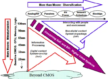
Fig. 10: Presentation of the IRDS roadmap. Even if the miniaturization still drives the semi-conductor industry (More Moore: miniaturization), the diversification towards several applications is desired (More than Moore). Combined together, this paves the way to higher value systems. Schematic from [22].
Targeting these future applications, the International Roadmap of Devices and Systems (IRDS) provides requirements for logic and memory technologies over a 15 years horizon. The main considered points are power, performance, area and cost (PPAC metric). According to their 2020 report, the main applications of nowadays logic technologies is high-performance and low-power/high density logic. Even with the improvement of lithographic tools, such as the extreme-ultraviolet (EUV) tools, the ground scaling is forecast to slow down and saturate around 2028. This traditional scaling must go with design-technology-co-optimization (DTCO) to reduce further the area limited by the design rules. Additionally, the standard transistor miniaturization is limited by parasitic elements but also by the prevalence of interconnections, which dictate nowadays the circuit delay. At the same time, power density poses a serious challenge, which when combined with the scaling of gate drive, could limit clock frequency at 0.8GHz in 2034. From this statement, a new paradigm has emerged, where microelectronics is no longer driven by PPAC but tends to diversify to propose added functionalities to standard devices (Fig. 10). This is called More than Moore applications and is not an alternative to Moore’s law but rather a complement to digital signal and data processing. From one hand, 3D monolithic integration (or sequential integration) by stacking transistors on top of the other, appears as an alternative to standard miniaturization to decrease further the delay between transistors, but also as a lever to add functionalities. This technology will be presented in the next sub-section. From the other hand, the limiting factor for performances is no longer the number of operations per second but rather the speed of communication between logic and memory chips and the associated energy. To break this memory
Page 22 wall, In-Memory computing proposes to gather memory and logic (computation) to reduce data movement and thus power consumption. It will be discussed in the second sub-section.
b. Introduction to 3D sequential integration
As previously stated, 3D sequential integration is interesting for More Moore and More than Moore applications. After a brief explanation of the technologies characteristics (which will be more detailed in Chapter II and III), we will see how 3D monolithic can be part of industrial roadmaps.
i. 3D sequential integration
3D sequential integration (3DSI), also called 3D monolithic integration consists in stacking active device layers on top of each other in a sequential manner. The sequential term is in opposition with parallel which described an integration (3D parallel integration or 3D packaging) where different chips are processed independently before being stacked and connected vertically. The connections between substrates can be done Through Silicon Via (TSV).
Fig. 11: Presentation of 3D Sequential Integration process flow.
Fig. 11 presents a typical 3D sequential integration process flow, where first the bottom MOSFET tier (bottom tier or tier 1) is processed and followed by the top active layer creation. It can be done either by direct deposition or wafer bonding. This step is detailed in chapter III. The final top active layer is thin enough to align the top transistor with the bottom level. Then the top layer is processed at low thermal budget (<500°C, 2hours) to avoid bottom tier degradation. Finally interconnections (3D contact) are done between the two tiers. Unlike TSV (diameter ~1.7µm), 3D contact detains dimensions similar to traditional ones, offering unique inter-tier connectivity opportunities thanks to precise alignment between tiers. In fact, the alignment accuracy is only limited by stepper resolutions [23]. As far as parallel integration is concerned the interconnection density is limited by the bonding alignment (around 200nm). Additionally, regarding the 3D contact dimensions, a high via density can be reached: over 100 million/mm² is projected with 14nm ground rules in [24].
To conclude this part, 3D monolithic integration enables the formation of multi-tier devices with a high interconnection density between the tiers that is not feasible in TSV technology. Next part will present why a dense interconnection network is required for More Moore applications.
ii. 3D sequential integration: More Moore applications
The first justification of 3DSI was to pursue Moore’s law and create an equivalent node by staking instead of shrinking transistors to improve circuit performances. Fig. 12 presents the granularity scale of stacking devices, 3DSI enabling a fine grain interconnection network between tiers that is not achieved with 3D parallel integration. In fact, for an identical silicon footprint (or die size), more devices will be integrated with shorter connections, improving the RC delay which dictates the circuit speed for advanced nodes (see Fig. 13). The gain of performances compared to planar devices are detailed in
Page 23 chapter II but in a nutshell Shi et al. [25] show that a transistor level partitioning in a 14nm technology node yields 20% improved performances among with 30% power saving compared to 2D IC [25].
.
Fig. 12: Definition of the different granularity scale for 3D integration, which are entire core, logic bloc, logic gates and transistor level. Due to the size of the contact, 3D parallel integration is limited to the first two level of abstractions while 3D sequential integration can cover the whole levels. This figure is taken from [26].
iii. 3D sequential integration: More than Moore Applications
In the scope of More than Moore applications, the idea is to integrate different layers types (analog layer, sensors and actuators, memory…) with 3D monolithic integration according to the targeted application. There is already done in other co-integration solutions like System-On-Chip but they are costly (large die size) and the process is not necessarily optimized for all signal domain (analog, digital…). Fig. 14 presents the advantages of heterogeneous integration, in particular 3D stacks to reduce system size, increase performances and reduce cost. Please note that 3D stack is not limited to 3D monolithic integration but can also comprise TSV technology, which, depending of the application, can be more relevant. For instance, we can think of a digital layer with an advanced CMOS node with high performances on top of an analog one with a relaxed node, which is less costly. The connections between analog and digital layers can be either fine grain or between entire blocks. Both technologies could be optimized for each applications (digital and analog in this example).
Fig. 13: Transistor and interconnection delay for sub 100nm nodes. Even if the transistor delay is reducing, the overall delay is dominated by back-End of Line (BEOL) RC. Reproduction from [27].
Fig. 14: Comparison between planar, System-On-Chip (SOC) and 3D stack to highlight advantages of heterogeneous integration. This figure is taken from [28].
Page 24 In this PhD manuscript we will tackle the topic of 3D monolithic technology from both design point of view and fabrication one. In fact, chapter II will describe Design-Technology Co-Optimization required to take all the benefits, in terms of performances, area and power from such a technology. Later, chapter III will propose the physical and electrical analysis of JL transistors and their low-temperature integration (<500°C), making them compatible with 3D monolithic integration. However, before going further, we will introduce In-Memory Computing applications, which do not rely on transistor miniaturization to gain performances but rather on gathering the memory block from computational one to reduce data transfer delay.
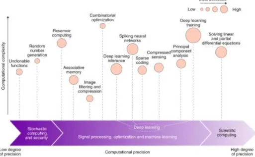
c. Introduction to In-Memory Computing:
The aim of this part is to provide general knowledge about In-Memory Computing, the context and their application field. For detailed information about the working principle, please refer to chapter IV. First, to present the pre-dominance of data access, various applications are presented in Fig. 15 according to data needs, computational complexity and computational precision. We do observe that either for security, deep learning or scientific applications, the data transfer between memory and computation part is primordial. However, this data exchange is translated into additional latency and power consumption for the well-known Von-Neumann architecture. In fact, due to this computing centric architecture -and not data-centric-, data movements in the memory hierarchy result in 50% energy waste [19] and is the main factor, limiting further improvements in computing performances. This limit is generally referred as the “memory wall”.
Fig. 15: Data access for various type of applications organised by computational precision and complexity. This figure is taken from [29].
To overcome this limitation, In/Near-Memory Computing (IMC/NMC) rises to be a solution with the co-location of data and logic operations, reducing drastically data movements. The idea is straightforward and illustrated in Fig. 16. In a Von-Neumann architecture, the processing unit will ask the memory block for the data, compute it and transfer again the result into the conventional memory. In an IMC system the processing unit will ask the computational memory block to perform the operations, whose results will be stocked directly into the memory array. For this, they exist several approaches based on charge or resistance memory devices. Several IMC approaches can be found in literature, shared between volatile (DRAM or SRAM) and non-volatile memory (Resistive memories as well as charge storage) with promising energy efficiency.
Page 25
Fig. 16: Illustration of Von-Neumann architecture and In-Memory Computing (IMC) one, taken from [29].
Chapter IV will explain what kind of computation operation can be performed in IMC architectures and propose an implementation of so-called “scouting logic” into a low-power high-density 3D cube.
Page 26
3- Thesis objectives:
This chapter presented the history of semiconductor industry as well as the current challenges. From the transistor miniaturisation trend enounced by Gordon E. Moore in 1965, a happy scaling era (with constant scaling factor between nodes) lasted until the 21 century. With the shrinking of dimensions, short channel effects limiting the device operation appeared. To mitigate them, boosters have been introduced and new device architectures rose. Nevertheless, digital circuit performance are no longer dictated by intrinsic transistor delay but rather by interconnections. At the same time, with the increase of transistor (and interconnection network) density, power consumption and dissipation is now an issue. From both aspects, 3D monolithic integration by staking transistors on top on the other can solve these issues by enabling shorter interconnections and lower silicon footprint. Chapter II will explore 3D monolithic designs to analyze the PPA gain from planar to 3D designs. For the manufacturing point of view, chapter III describes the fabrication of low-temperature junctionless transistors and their electrical characterization. Additionally, it is also possible to merge memory and computational part to avoid data transfers (i.e save energy) through separated blocks. In-Memory computing is foreseen as an alternative to Von-Neumann architecture for efficient and low power computation. In this scope, Chapter IV proposes a low-power high-density 3D cube. Simulations based on experimental data demonstrates Boolean operation feasibility.
The main topics tackled in this manuscript are: Chapter II:
Proposition of a 3D VLSI design flow.
How to share resources between different tiers? How efficient is the partitioning?
Can we take benefit from the 3D architecture to integrate back-planes for top-tier transistors? SRAM as physically unclonable functions.
Chapter III:
TCAD comparison of JL devices, n/p devices and inversion-mode one. Description of junctionless devices process flow at low-temperature.
Electrical characterization of Juncrionless and Inversion-Mode devices (analog applications, digital FOM and variability).
Chapter IV:
Introduction of a 3D cube co-integrating junctionless nanowires and memory elements for IMC through “Scouting Logic”.
Choice and sizing of the materials. Presentation of the process flow.
Page 27
Chapter II: Design Technology Co-Optimization:
functionalities provided by 3D monolithic
integration
3D monolithic integration is foreseen as an alternative to traditional transistor scaling to pursue Moore’s law. Stacking devices with a fine grain contact grid between tiers allows the reduction of the wire length and could leverage new architectures improving both performance, power and silicon footprint. The aim of this chapter is to optimize 3D structure design with such a technology and quantify the gain provided. In the first part, the VLSI digital planar design flow is presented with insights and modifications required to create a 3D one. In the second part, the state of the art of 3D design assessment is done in terms of performance, power consumption and area. In the third part, the 3D environment used in this PhD work is presented. Then, 3D monolithic routing, wire decongestion and design guidelines of back gate contact are discussed. Afterwards, a specific assist technic for 3D monolithic SRAM is proposed to compensate SRAM deviation from reference one. This technic is enabled by a specific feature of this technology: the back gate integration. To finish with, variability in SRAM is used as an asset to generate physical unclonable function for security purposes.
1- VLSI digital design flow ... 29 a. Overview of a planar digital design flow and EDA tools ... 29 b. Power, performance and area (PPA) design trade-off ... 32 c. From 2D to 3D digital design flow... 33 i. 3D Design flow ... 33 ii. Netlist partitioning: examples ... 33 2- State of the art of 3D design performance assessment: Motivation for 3D monolithic integration for digital applications ... 35 a. Cost analysis ... 35 b. Thermal dissipation issue ... 35 c. Performances ... 37 3- 3D design MOSFET environment ... 39 a. 3D tier and intermediate BEOL for CMOS over CMOS integration: Coolcube TM ... 39 b. SPICE model ... 40 c. Parasitic element extraction ... 40 d. Methodology summary ... 41 e. RO, SRAM benchmark: typical figure of merits ... 42 i. Ring Oscillator ... 42 ii. SRAM ... 42 4- Routing in 3D designs ... 45 a. Buried power rail ... 45
Page 28 b. Congestion mitigation and resources sharing between tiers ... 45 c. Design guidelines for top-tier Back-plane contact ... 48 i. Simulated structure ... 48 ii. Static consideration ... 49 iii. Dynamic consideration ... 50 5- Design-technology co-optimization: top-tier SRAM ... 51 a. 14nm technology performance ... 51 i. Electrical characterization of typical FOM ... 51 ii. SRAM: variability issue and impact on FOM ... 53 iii. Back-bias assist ... 54 iv. BTI-induced dynamic variability at the bitcell level ... 55 a- BTI mechanism ... 55 b. BTI at the bitcell level: experimental results ... 56 c. Proposition of a novel fine-grain back-bias assist techniques for 3D-monolithic 14nm FDSOI top-tier SRAMs ... 59 i. 3D monolithic design kit: layout considerations ... 59 ii. Fine grain and versatile back-bias assist ... 60 iii. Parasitic capacitances reduction ... 63 6- Variability as an asset: FDSOI SRAM PUF ... 65 a. PUF: SRAM based fingerprint ... 65 b. Single dopant transport ... 66 c. Emulation of leaky devices to assist technological choices ... 66 i. Impact of channel doping on SRAM devices ... 67 ii. Simulation environment ... 67 iii. Emulation of resonant transport ... 71 iv. Conclusion: ... 73 7- Conclusion of chapter II ... 74
Page 29
1- VLSI digital design flow
First, this part presents the VLSI planar design flow commonly used to design complex circuits. Then, an emphasis is done on power, performance and area (PPA) metrics. To finish, the adaptation of the planar design flow for 3D monolithic technology is presented.
a. Overview of a planar digital design flow and EDA tools
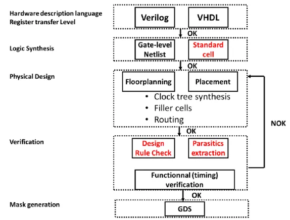
With an increasing number of transistors to manage, the Very Large Scale Integration (VLSI) design flow has become automated. It is composed of various sequential stages with a high level of abstraction to build complex circuit up to billion of transistors. Fig. 17 presents the sequential steps to generate the layout. Let’s consider the example of a ring oscillator to explain the different building blocks.
Fig. 17: Usual planar design flow. The part tackled in this work are highlighted in red.
A ring oscillator (RO) is a device composed of an odd number of NOT gates (inverters) in a ring. The output oscillates between two voltage levels, representing true (noted 0) and false (noted 1). The NOT gates, or inverters, are attached in a chain and the output of the last inverter is fed back into the first. A three stage RO is presented in Fig. 18 and its ideal output in Fig. 19.
Fig. 18: Example of a three ring inverter. The output frequency depends on the inverter delay τ and is 1/6.τ.
Fig. 19: Schematic of the desired waveform output. An oscillation is expected from a low state (gnd, ‘0’) to a high state (VDD, ‘1’).
One practical way to represent this ring oscillator is to code it using a hardware descriptive language (HDL) like in Fig. 20. For instance, Verilog or VHDL can be used to model a synchronous digital circuit in terms of the flow of digital signals (data) between hardware registers, and the logical operations
Page 30 performed on those signals. The described circuit is usually synchronous, i.e. the change of state of each memory element is regulated by a clock signal.
library ieee;
use ieee.std_logic_1164.all; entity ring_oscillator is port (ro_en : in std_logic; delay : in time;
ro_out : out std_logic); end ring_oscillator;
architecture behavioral of ring_osc is
signal gate_out : std_logic_vector(2 downto 0) := (others => '0');
begin process begin
gate_out(0) <= ro_en and gate_out(2); wait for delay;
gate_out(1) <= not(gate_out(0)); wait for delay;
gate_out(2) <= not(gate_out(1)); wait for delay;
ro_out <= gate_out(2); end process;
end behavioral;
Fig. 20: This three inverter ring oscillator code is given as an example. The input/output ports are highlighted in red. The input delay have been added to be able to simulate the RO at this stage. Also, when the logic is synthetized without specific constraints, the redundant logic cell are suppressed and the ring oscillator described above will be replaced by a single inverter.
Then, the synthesis tool considers the combinational and sequential logic described by the HDL at the RTL level and synthesises the logic. It means that the RTL blocks are associated to the smallest level constructs called standard cells. The standard cells come from a library and perform specific operation. For instance, an inverter (Boolean function NOT) with input I and output O can be a standard cell. More complex structure such as 2-bit full adder are also available in the standard cell library. The layout of standard cell are fixed height (but variable width) to ease their future placement in rows. For instance for the 14nm, the standard cell height is 880nm, delimited by power rails. They are optimized full custom layout, minimizing delay and area. Usually they are designed by the Application Specific Integrated Circuit (ASIC) manufacturer and are presented under several views such as symbols or electrical schematics (see Fig. 21). The final collection of standard cells and the required electrical connections between them is called a gate-level netlist. A timing analysis can be done at this stage to ensure the proper operation of the circuit.
Page 31
(a) (b) (c)
Fig. 21: Different representation for the same entity (a) Electrical schematics of an inverter taken from [30]. The NMOS and PMOS are represented and the pin in blue materialized the input port (A) and in red the output port (Z). (b) Symbolic representation, the inverter is seen as a black box with input (A) and output (Z). Behind this representation, the circuit in (a) is implemented. That is why this entity can be directly used in more complex circuit. (c) Associated layout of the inverter.
After, the physical design consists in placing and optimizing the gate position of the netlist on a floorplan. It is possible to define a specific partitioning to separate some blocks from the others. Once the gates are physically placed, the clock tree is synthesised to drive correctly the flip-flops and minimize the skew and insertion delay. Filler cells complete the unused space to ensure performance and reliability. Then, the root tool will make physical connections between the standard cells with back-end metal rails and via. Usually, the wire length is minimized to avoid additional delay but should not lead to a wire congestion. An example of the obtained layout is presented in Fig. 22. From a general point of view, all the tools search to reduce area, timing (increase performance) and power consumption. Some specific requirement can be done on a constraint (maximum power consumption for instance) at the expense of the others. However, if the constraints are too restricted, the place and root tool cannot find a solution and a trade-off between power, performance and area must be figured out.
Fig. 22: Example of a layout combining several Ring-oscillators, physical random number generation taken from [31].
Final physical verifications are done prior mask generation. For instance, a Design Rule Check (DRC) ensure that the generated layout respect the design restrictions for device processing. As an example, the DRC contains spacing rules between metallic layers to make sure that they are electrically independent. A specific DRC is done for each technology. Also, the circuit timing is verified (and thus proper circuit operation is ensured) considering all the parasitic elements (capacitance, RC wire delay…). Waveforms function can be generated for timing analysis. Note that similar verifications are done for each step of the design process flow but are not detailed.
To finish, the Graphic Design System (GDS) is generated. It is a binary file format which represents planar geometric shapes, text labels, and other information about the layout. It can be directly used to generate masks for future device processing.
![Fig. 7: FDSOI transistor TEM cross-section developed for the 22nm node. Figure from [14]](https://thumb-eu.123doks.com/thumbv2/123doknet/14546829.725400/21.892.118.747.434.623/fig-fdsoi-transistor-tem-cross-section-developed-figure.webp)
![Fig. 16: Illustration of Von-Neumann architecture and In-Memory Computing (IMC) one, taken from [29]](https://thumb-eu.123doks.com/thumbv2/123doknet/14546829.725400/27.892.238.655.111.470/fig-illustration-von-neumann-architecture-memory-computing-taken.webp)
![Fig. 21: Different representation for the same entity (a) Electrical schematics of an inverter taken from [30]](https://thumb-eu.123doks.com/thumbv2/123doknet/14546829.725400/33.892.114.778.104.313/fig-different-representation-entity-electrical-schematics-inverter-taken.webp)
![Fig. 28: DRM showing upper level tier, with MI4 iBEOL level, back- back-gate, top tier FEOL and BEOL, taken from [80]](https://thumb-eu.123doks.com/thumbv2/123doknet/14546829.725400/43.892.115.782.106.388/showing-upper-level-ibeol-level-feol-beol-taken.webp)